EP0803945A2 - Hybrid mirror structure for a visible emitting VCSEL - Google Patents
Hybrid mirror structure for a visible emitting VCSEL Download PDFInfo
- Publication number
- EP0803945A2 EP0803945A2 EP97106549A EP97106549A EP0803945A2 EP 0803945 A2 EP0803945 A2 EP 0803945A2 EP 97106549 A EP97106549 A EP 97106549A EP 97106549 A EP97106549 A EP 97106549A EP 0803945 A2 EP0803945 A2 EP 0803945A2
- Authority
- EP
- European Patent Office
- Prior art keywords
- alternating layers
- pairs
- bragg reflector
- distributed bragg
- layers
- Prior art date
- Legal status (The legal status is an assumption and is not a legal conclusion. Google has not performed a legal analysis and makes no representation as to the accuracy of the status listed.)
- Withdrawn
Links
- 238000005253 cladding Methods 0.000 claims abstract description 26
- 239000000758 substrate Substances 0.000 claims abstract description 16
- 239000000463 material Substances 0.000 claims abstract description 14
- 229910052782 aluminium Inorganic materials 0.000 claims abstract description 11
- XAGFODPZIPBFFR-UHFFFAOYSA-N aluminium Chemical compound [Al] XAGFODPZIPBFFR-UHFFFAOYSA-N 0.000 claims abstract description 11
- 229910000980 Aluminium gallium arsenide Inorganic materials 0.000 claims description 2
- 239000010410 layer Substances 0.000 description 100
- 238000002310 reflectometry Methods 0.000 description 18
- MDPILPRLPQYEEN-UHFFFAOYSA-N aluminium arsenide Chemical compound [As]#[Al] MDPILPRLPQYEEN-UHFFFAOYSA-N 0.000 description 12
- AUCDRFABNLOFRE-UHFFFAOYSA-N alumane;indium Chemical compound [AlH3].[In] AUCDRFABNLOFRE-UHFFFAOYSA-N 0.000 description 11
- FTWRSWRBSVXQPI-UHFFFAOYSA-N alumanylidynearsane;gallanylidynearsane Chemical compound [As]#[Al].[As]#[Ga] FTWRSWRBSVXQPI-UHFFFAOYSA-N 0.000 description 11
- 238000004519 manufacturing process Methods 0.000 description 11
- 238000000034 method Methods 0.000 description 10
- 230000003647 oxidation Effects 0.000 description 10
- 238000007254 oxidation reaction Methods 0.000 description 10
- 229910005540 GaP Inorganic materials 0.000 description 7
- 229910001218 Gallium arsenide Inorganic materials 0.000 description 7
- 238000001429 visible spectrum Methods 0.000 description 7
- JBRZTFJDHDCESZ-UHFFFAOYSA-N AsGa Chemical compound [As]#[Ga] JBRZTFJDHDCESZ-UHFFFAOYSA-N 0.000 description 6
- 239000002019 doping agent Substances 0.000 description 6
- HZXMRANICFIONG-UHFFFAOYSA-N gallium phosphide Chemical compound [Ga]#P HZXMRANICFIONG-UHFFFAOYSA-N 0.000 description 6
- 230000000873 masking effect Effects 0.000 description 6
- 239000004065 semiconductor Substances 0.000 description 5
- 238000005530 etching Methods 0.000 description 4
- GYHNNYVSQQEPJS-UHFFFAOYSA-N Gallium Chemical compound [Ga] GYHNNYVSQQEPJS-UHFFFAOYSA-N 0.000 description 3
- 238000013459 approach Methods 0.000 description 3
- 238000000151 deposition Methods 0.000 description 3
- 229910052733 gallium Inorganic materials 0.000 description 3
- 229910052738 indium Inorganic materials 0.000 description 3
- APFVFJFRJDLVQX-UHFFFAOYSA-N indium atom Chemical compound [In] APFVFJFRJDLVQX-UHFFFAOYSA-N 0.000 description 3
- 230000003287 optical effect Effects 0.000 description 3
- 230000008569 process Effects 0.000 description 3
- 238000003491 array Methods 0.000 description 2
- 230000007547 defect Effects 0.000 description 2
- 230000008021 deposition Effects 0.000 description 2
- 229910052751 metal Inorganic materials 0.000 description 2
- 239000002184 metal Substances 0.000 description 2
- 230000004048 modification Effects 0.000 description 2
- 238000012986 modification Methods 0.000 description 2
- BASFCYQUMIYNBI-UHFFFAOYSA-N platinum Chemical compound [Pt] BASFCYQUMIYNBI-UHFFFAOYSA-N 0.000 description 2
- 229910052710 silicon Inorganic materials 0.000 description 2
- 239000010703 silicon Substances 0.000 description 2
- 239000002356 single layer Substances 0.000 description 2
- -1 AlAs/Al.5Ga.5As) Chemical compound 0.000 description 1
- OKTJSMMVPCPJKN-UHFFFAOYSA-N Carbon Chemical compound [C] OKTJSMMVPCPJKN-UHFFFAOYSA-N 0.000 description 1
- 208000033991 Device difficult to use Diseases 0.000 description 1
- BUGBHKTXTAQXES-UHFFFAOYSA-N Selenium Chemical compound [Se] BUGBHKTXTAQXES-UHFFFAOYSA-N 0.000 description 1
- HCHKCACWOHOZIP-UHFFFAOYSA-N Zinc Chemical compound [Zn] HCHKCACWOHOZIP-UHFFFAOYSA-N 0.000 description 1
- RNQKDQAVIXDKAG-UHFFFAOYSA-N aluminum gallium Chemical compound [Al].[Ga] RNQKDQAVIXDKAG-UHFFFAOYSA-N 0.000 description 1
- 229910052799 carbon Inorganic materials 0.000 description 1
- 230000008859 change Effects 0.000 description 1
- 238000005229 chemical vapour deposition Methods 0.000 description 1
- 238000004891 communication Methods 0.000 description 1
- 150000001875 compounds Chemical class 0.000 description 1
- 239000004020 conductor Substances 0.000 description 1
- PCHJSUWPFVWCPO-UHFFFAOYSA-N gold Chemical compound [Au] PCHJSUWPFVWCPO-UHFFFAOYSA-N 0.000 description 1
- 229910052737 gold Inorganic materials 0.000 description 1
- 239000010931 gold Substances 0.000 description 1
- 230000003116 impacting effect Effects 0.000 description 1
- 230000006872 improvement Effects 0.000 description 1
- AMGQUBHHOARCQH-UHFFFAOYSA-N indium;oxotin Chemical compound [In].[Sn]=O AMGQUBHHOARCQH-UHFFFAOYSA-N 0.000 description 1
- 230000005012 migration Effects 0.000 description 1
- 238000013508 migration Methods 0.000 description 1
- 238000001451 molecular beam epitaxy Methods 0.000 description 1
- 150000004767 nitrides Chemical class 0.000 description 1
- 230000001590 oxidative effect Effects 0.000 description 1
- 238000000059 patterning Methods 0.000 description 1
- 229920002120 photoresistant polymer Polymers 0.000 description 1
- 229910052697 platinum Inorganic materials 0.000 description 1
- 238000012545 processing Methods 0.000 description 1
- 230000004044 response Effects 0.000 description 1
- 229910052711 selenium Inorganic materials 0.000 description 1
- 239000011669 selenium Substances 0.000 description 1
- 229910052725 zinc Inorganic materials 0.000 description 1
- 239000011701 zinc Substances 0.000 description 1
Images

Classifications
-
- H—ELECTRICITY
- H01—ELECTRIC ELEMENTS
- H01S—DEVICES USING THE PROCESS OF LIGHT AMPLIFICATION BY STIMULATED EMISSION OF RADIATION [LASER] TO AMPLIFY OR GENERATE LIGHT; DEVICES USING STIMULATED EMISSION OF ELECTROMAGNETIC RADIATION IN WAVE RANGES OTHER THAN OPTICAL
- H01S3/00—Lasers, i.e. devices using stimulated emission of electromagnetic radiation in the infrared, visible or ultraviolet wave range
-
- H—ELECTRICITY
- H01—ELECTRIC ELEMENTS
- H01S—DEVICES USING THE PROCESS OF LIGHT AMPLIFICATION BY STIMULATED EMISSION OF RADIATION [LASER] TO AMPLIFY OR GENERATE LIGHT; DEVICES USING STIMULATED EMISSION OF ELECTROMAGNETIC RADIATION IN WAVE RANGES OTHER THAN OPTICAL
- H01S5/00—Semiconductor lasers
- H01S5/10—Construction or shape of the optical resonator, e.g. extended or external cavity, coupled cavities, bent-guide, varying width, thickness or composition of the active region
- H01S5/18—Surface-emitting [SE] lasers, e.g. having both horizontal and vertical cavities
- H01S5/183—Surface-emitting [SE] lasers, e.g. having both horizontal and vertical cavities having only vertical cavities, e.g. vertical cavity surface-emitting lasers [VCSEL]
- H01S5/18361—Structure of the reflectors, e.g. hybrid mirrors
- H01S5/18377—Structure of the reflectors, e.g. hybrid mirrors comprising layers of different kind of materials, e.g. combinations of semiconducting with dielectric or metallic layers
-
- H—ELECTRICITY
- H01—ELECTRIC ELEMENTS
- H01S—DEVICES USING THE PROCESS OF LIGHT AMPLIFICATION BY STIMULATED EMISSION OF RADIATION [LASER] TO AMPLIFY OR GENERATE LIGHT; DEVICES USING STIMULATED EMISSION OF ELECTROMAGNETIC RADIATION IN WAVE RANGES OTHER THAN OPTICAL
- H01S5/00—Semiconductor lasers
- H01S5/10—Construction or shape of the optical resonator, e.g. extended or external cavity, coupled cavities, bent-guide, varying width, thickness or composition of the active region
- H01S5/18—Surface-emitting [SE] lasers, e.g. having both horizontal and vertical cavities
- H01S5/183—Surface-emitting [SE] lasers, e.g. having both horizontal and vertical cavities having only vertical cavities, e.g. vertical cavity surface-emitting lasers [VCSEL]
- H01S5/18361—Structure of the reflectors, e.g. hybrid mirrors
- H01S5/18369—Structure of the reflectors, e.g. hybrid mirrors based on dielectric materials
- H01S5/18372—Structure of the reflectors, e.g. hybrid mirrors based on dielectric materials by native oxidation
Definitions
- This invention relates, in general, to layered optical devices and, more particularly, to semiconductor lasers.
- edge emitting semiconductor lasers play a significant role in optical communication due to their high operating efficiency and modulation capabilities; however, the edge emitting semiconductor lasers have several short comings or problems, thus making the edge emitting laser device difficult to use in several applications.
- VCSEL vertical cavity surface emitting lasers
- the conventional VCSEL has several advantages, such as emitting light perpendicular to the surface of the die, and the possibility of fabrication of two dimensional arrays.
- conventional VCSELs have several advantages
- conventional VCSELs have several disadvantages with regard to emission in the visible spectrum primarily due to the poor reflectivity of the distributed Bragg reflectors. Because of this, manufacturability of VCSELs for the visible spectrum is severely limited.
- reflectivity problems are solved by increasing the number of reflective elements or alternating layers that comprise the conventional distributed Bragg reflectors.
- this approach may not solve the reflectivity problems (due to increased reflector losses and narrowing of the bandwidth of the reflector), but exacerbates several other problems, such as manufacturability, defect density, higher resistance and the like, thus making the conventional approach not a viable solution to the problem.
- alternating layers e.g., as many as 50 to 200 additional alternating layers
- increasing the number of alternating layers increases the cost and complexity of manufacturing. More particularly, with the increased number of alternating layers, an increase in defect density of the alternating layers may be produced, as well as an increase in the amount of time required to manufacture the layers. Also, the series resistance increases with increased alternating layers, potentially impacting the temperature performance of the device.
- FIG. 1 illustrates a simplified enlarged vertical cavity surface emitting laser (VCSEL) 101 formed on a substrate 102 having surfaces 103 and 104 with light 120 being emitted from VCSEL 101. It should be understood that while FIG. 1 only illustrates a single VCSEL 101, VCSEL 101 may represent many VCSELs that are located on substrate 102 to form arrays.
- VCSEL vertical cavity surface emitting laser
- VCSEL 101 is made of several defined areas or regions, such as a distributed Bragg reflector 106 having a plurality of alternating layers 108 illustrated by layers 111 and 113 and a plurality of alternating layers 116 illustrated by layers 118 and 119, a cladding region 123, an active region 126, a cladding region 128, a distributed Bragg reflector 130 having a plurality of alternating layers 131 illustrated by layers 133 and 135, and a contact region 140.
- a distributed Bragg reflector 106 having a plurality of alternating layers 108 illustrated by layers 111 and 113 and a plurality of alternating layers 116 illustrated by layers 118 and 119
- a cladding region 123 an active region 126
- a cladding region 128 a distributed Bragg reflector 130 having a plurality of alternating layers 131 illustrated by layers 133 and 135, and a contact region 140.
- Substrate 102 in this example, is made of any suitable material, such as gallium arsenide, silicon, or the like. Typically, substrate 102 is made of gallium arsenide so as to facilitate epitaxial growth of subsequent multiple layers that comprise VCSEL 101.
- any suitable epitaxial deposition method such as molecular beam epitaxy (MBE), metal organic chemical vapor deposition (MOCVD), or the like is used to deposit the required multiple layered structures, such as distributed Bragg reflector 106, having the plurality of alternating layers 108 and the plurality of alternating layers 116, cladding region 123, active region 126, cladding region 128, distributed Bragg reflector 130, and a contact region 140 for VCSEL 101.
- MBE molecular beam epitaxy
- MOCVD metal organic chemical vapor deposition
- these layers are made of compound semiconductor materials, such as indium aluminum gallium phosphide, aluminum arsenide, gallium arsenide, aluminum gallium arsenide, aluminum gallium phosphide, indium aluminum phosphide, and the like. It should be understood that epitaxial deposition is used extensively to produce the multitude of layers that comprise the VCSEL 101.
- thicknesses of the plurality of alternating layers 106, the plurality of alternating layers 130, cladding region 123, cladding region 128, active region 126, and contact region 140 are set out as portions of a wavelength of light 120 being emitted by VCSEL 101.
- optical thickness of each alternating layer 133, and 135 is set at 167.5 nanometers, thereby making the thickness of each alternating layer 133, and 135 one quarter of the wavelength of light 120 being emitted from VCSEL 101.
- the plurality of alternating layers 116 form a standard section of the lower Bragg reflector.
- the plurality of alternating layers 108 form an additional section of the lower Bragg reflector.
- One layer in each segment (pair) of alternating layers 108 is selectively oxidized (to be explained).
- the thickness of the oxidized layers is chosen such that it is one quarter wavelength after oxidation. Additionally, it should be understood that other thicknesses or portions of the wavelength can be used such as, one half, three quarter, or any multiple thereof.
- Doping of VCSEL 101 is achieved by the addition of dopant materials, e.g., n-type dopants and p-type dopants to epitaxial materials used for epitaxial deposition, thereby doping the epitaxially deposited material.
- dopant materials e.g., n-type dopants and p-type dopants
- alternating layers 116 of distributed Bragg reflector 106 are n-type doped with selenium, silicon, or the like to a concentration ranging from 1E15 to 1E20 cm -3 , with a preferred range from 1E17 to 1E19 cm -3 , with a nominal range from 5E17 to 1E18 cm -3
- distributed Bragg reflector 130 is p-type doped with carbon, zinc, or the like to a concentration ranging from 1E15 to 1E20 cm -3 , with a preferred range from 1E17 to 1E19 cm -3 , and a nominal range from 1E18 to 5E18 cm -3 .
- Distributed Bragg reflector 106 is made of the plurality of alternating layers 108 and the plurality of alternating layers 116. As stated earlier, the plurality of alternating layers 108 will be oxidized during processing to form a highly reflective partial mirror.
- the plurality of alternating layers 108 further include one or more layers of aluminum arsenide, illustrated by a layer 111, and one or more layers of aluminum gallium arsenide, illustrated by a layer 113.
- layer 111 of aluminum arsenide e.g., AlAs
- layer 113 of aluminum gallium arsenide e.g., Al .5 Ga .5 As
- layer 111 aluminum arsenide
- layer 113 of aluminum gallium arsenide e.g., Al .5 Ga .5 As
- layer 111 aluminum arsenide
- layer 113 aluminum gallium arsenide
- reflectors e.g., AlAs/Al .5 Ga .5 As
- alternating layers 108 can have from one pair to twenty pair of mirrors, with a preferred number of pairs ranging from three to ten pairs, and with a nominal number of pairs being four to six pairs. Additionally, applicant believes that five mirrored pairs of aluminum arsenide and aluminum gallium arsenide give an appropriate reflectivity performance for VCSEL 101 operating in the visible spectrum once oxidation has taken place in the fabrication sequence. However, it should be understood that the number of alternating layers 111 and 113 can be adjusted for specific applications. Also, it should be noted that layer 114 is made of aluminum arsenide and forms a top layer for alternating layers 108. It should be further understood that in the examples where a percent composition of a particular element is given it should be considered only as an example and that these variations from these examples can be large and are also part of the present invention.
- the aluminum and the gallium of the aluminum gallium arsenide can be varied.
- the aluminum of the aluminum gallium arsenide can range from 0 percent to 100 percent, with a preferred range from 46 percent to 54 percent in Al .5 Ga .5 As
- the plurality of alternating layers 116 are epitaxially deposited on the plurality of alternating layers 108.
- the plurality of alternating layers 116 further include one or more layers of indium aluminum gallium phosphide, illustrated as a layer 118, and one or more layers of indium aluminum phosphide, illustrated by a layer 119.
- layer 118 of indium aluminum gallium phosphide e.g., In .49 Al .1 Ga .41 P
- layer 114 of indium aluminum phosphide is deposed on layer 114 with a subsequent layer 119 of indium aluminum phosphide (e.g., In .49 Al .51 P) being deposited on the indium aluminum gallium phosphide layer 118, thereby making another mirror pair.
- the plurality of alternating layers 116 can range from one pair to twenty pair of mirror pairs, with a preferred number of pairs being from three to ten, and with a nominal number of pairs being four to six. It is believed that five mirrored pairs of indium aluminum gallium arsenide and indium aluminum phosphide, in conjunction with the plurality of alternating layers 108, give appropriate reflectivity performance for VCSEL 101 operating in the visible spectrum. In addition to increasing the reflectivity of distributed Bragg reflector 106, alternating layers 116 provide an N-metal contact for VCSEL 101 and inhance the reliability of VCSEL 101 by including indium, which aids in preventing the migration of dislocations and the like to active region 126. However, it should be understood that the number of alternating layers 118 and 119 can be adjusted for specific applications.
- reflectivity from the indium aluminum gallium phosphide can be achieved by having a percent composition of indium ranging from 46 percent to 54 percent. By varying the percent composition of indium, a corresponding variation in a percent composition of gallium occurs. Additionally, aluminum percent concentration can range from 1 percent to 20 percent with a nominal range from 7 percent to 13 percent. It should be pointed out that the percent composition of the aluminum reduces the percent concentration of gallium, thereby producing a balanced composition.
- cladding regions 123 and 128 are each shown as a single layer; however, it should be understood that each cladding region 123 and 128 can be made of more than one layer epitaxially disposed or deposited on a previous layer (e.g. Bragg reflector 106 and active region 126), with cladding layers 123 and 128 being made of any suitable doped or undoped material such as undoped indium aluminum gallium phosphide epitaxially deposited.
- active region 126 is represented by a single layer which is epitaxially deposited or disposed on cladding region 123; however, it should be understood that active region 126 can include one or more quantum wells, etc.
- Distributed Bragg reflector 130 is made of the plurality of alternating layers 131.
- the plurality of alternating layers 130 further include one or more layers of aluminum arsenide, illustrated by a layer 133, and one or more layers of aluminum gallium arsenide, illustrated by a layer 135.
- a layer of aluminum arsenide e.g., AlAs
- AlAs aluminum arsenide
- a layer of aluminum arsenide e.g., AlAs
- Al .5 Ga .5 As aluminum gallium arsenide
- another mirror pair or another pair of reflectors e.g., AlAs/Al .5 Ga .5 As.
- additional mirror pairs are required, several more layers, i.e., additionally mirror pairs are deposited on the existing layers of aluminum arsenide and aluminum gallium arsenide.
- the plurality of alternating layers 130 are from one pair to fifty mirror pairs, with a preferred number of mirror pairs ranging from ten to forty pairs, and with a nominal number of mirror pairs ranging from twenty to thirty mirrored pairs, and an optimum number of twenty eight mirror pairs. However, it should be understood that the number of mirror pairs can be adjusted for specific applications.
- a heavily doped contact layer 140 is formed on the upper surface of distributed Bragg reflector 130 and an electrical contact (not shown) is formed on layer 140 by disposing any suitable conductive material on layer 140, such as indium tin oxide, gold, platinum, or the like. It should be understood that depending upon which material selection is made the specific method of disposing and patterning of that specific material will change to form contact layer 140 and the electrical contact.
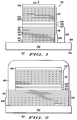
- FIGS. 2 and 3 some steps in a specific process for the fabrication of VCSEL 101 are illustrated. It will of course be understood that other methods might be utilized and the procedure to be described is simply for purposes of example and explanation. Components of the structures in FIGS. 2 and 3 which are similar to components previously illustrated and described in conjunction with FIG. 1 are designated with similar numbers.
- substrate 102 is illustrated with first distributed Bragg reflector 106 deposited thereon.
- Cladding region 123, active region 126 and cladding region 128 are deposited on the upper surface of distributed Bragg reflector 106 as previously described.
- Distributed Bragg reflector 130 is deposited on the upper surface of cladding region 128.
- cladding region 123, active region 126, cladding region 128 and distributed Bragg reflector 130 are etched to define VCSEL 101 but the diameter is still substantially larger than the operating cavity region so that active region 126 will not be damaged by this etching step.
- a masking layer 150 is deposited over the entire structure.
- Masking layer 150 can be any material which is sufficiently impervious to the following etch and oxidation steps, e.g. photoresist, oxides, nitrides, etc.
- Masking layer 150 is then etched, or otherwise removed, to define a diameter or lateral extent for distributed Bragg reflector 106.
- substrate 102 is etched to expose the edge of distributed Bragg reflector 106, with the diameter of distributed Bragg reflector 106 being larger than the diameter of cladding region 123, active region 126, cladding region 128 and distributed Bragg reflector 130 by the thickness of masking layer 150.
- the etched wafer is subjected to oxidation environment, thereby oxidizing the aluminum found in alternating layers 108 of distributed Bragg reflector 106 of VCSEL 101.
- Stack 108 oxidizes preferentially due to higher aluminum content.
- the oxidation speed of AlAs is much faster than that of AlGaAs. Only the AlAs layers in alternating layers 108 are oxidized because masking layer 150 protects any AlAs layers of distributed Bragg reflector 130. Oxidation of the aluminum in VCSEL 101 is achieved by any suitable method, such as steam oxidation, high pressure oxidation, or the like.
- process parameters are system specific and can range widely from system to system.
- oxidation can be carried out at temperatures ranging from 100 degrees Celsius to 700 degrees Celsius, with pressure ranging from 0.01 atmosphere to 10 atmospheres.
- Aluminum arsenide layers 111 in distributed Bragg reflector 106 are substantially completely oxidized, thus their index of refraction drops from approximately 2.9 to a range between 1.3 to 1.7, and nominally to 1.55.
- FIG. 3 A typical example of this procedure is described in U.S. Patent No. 5,258,316, entitled “Patterned Mirror Vertical Cavity Surface Emitting Laser” issued November 2, 1993 and assigned to the same assignee.
- Broken lines 151 are included in the structure of FIG. 3, to define the portion of FIG. 3 which is illustrated in FIG. 1. It will of course be understood by those skilled in the art that in some applications the structure illustrated in FIG. 1 may be the entire structure and other fabrication methods may be utilized.
- a dielectric layer 152 and an electrical contact layer 155 are applied to complete VCSEL 101.
- VCSEL 101 is a top emitting laser so that electrical contact layer 155 is formed to define an emitting window or aperture therethrough.
- many other types of electrical contacts may be utilized and the present structure is illustrated only for purposes of explanation.
- a reflectivity curve 201 is illustrated, having portions 202, 203, 204, representative of the reflectivity for distributed Bragg reflector 106 of VCSEL 101 with substrate 102 being made of gallium arsenide, with five mirrored pairs of the plurality of alternating layers 108 being made of AlAs (Oxidized)/Al 0.5 Ga 0.5 As, and with five mirrored pairs of the plurality of alternating layers 116 being made of (In 0.49 Al 0.1 Ga 0.41 P/In 0.49 Al 0.51 P).
- reflectivity of distributed Bragg reflector 106 of VCSEL 101 is illustrated throughout the visible spectrum, i.e., 550 nanometers to 900 nanometers. As can be seen by portion 202, reflectivity of distributed Bragg reflector 106 sharply increases and exceeds ninety percent at approximately 570 nanometers. At approximately, 600 nanometers reflectivity is in excess of 95.0 percent. In general, portion 203 illustrates reflectivity that is in excess of 99.9 percent that is from 640 nanometers to 840 nanometers. Portion 203 illustrates a wide response curve with exceptionally good reflectivity in the visible spectrum. Portion 204 illustrates a sharply declining side of the reflectivity curve 201. Thus, making distributed Bragg reflector 106 of VCSEL 101 extremely effective for reflecting light 120 that is in the visible spectrum.
Landscapes
- Physics & Mathematics (AREA)
- Electromagnetism (AREA)
- Optics & Photonics (AREA)
- Condensed Matter Physics & Semiconductors (AREA)
- General Physics & Mathematics (AREA)
- Engineering & Computer Science (AREA)
- Plasma & Fusion (AREA)
- Semiconductor Lasers (AREA)
- Optical Elements Other Than Lenses (AREA)
Abstract
Description
- This invention relates, in general, to layered optical devices and, more particularly, to semiconductor lasers.
- At present, conventional edge emitting semiconductor lasers play a significant role in optical communication due to their high operating efficiency and modulation capabilities; however, the edge emitting semiconductor lasers have several short comings or problems, thus making the edge emitting laser device difficult to use in several applications.
- Recently, however, there has been an increased interest in vertical cavity surface emitting lasers (VCSEL)s. The conventional VCSEL has several advantages, such as emitting light perpendicular to the surface of the die, and the possibility of fabrication of two dimensional arrays. However, while conventional VCSELs have several advantages, conventional VCSELs have several disadvantages with regard to emission in the visible spectrum primarily due to the poor reflectivity of the distributed Bragg reflectors. Because of this, manufacturability of VCSELs for the visible spectrum is severely limited.
- Conventionally, reflectivity problems are solved by increasing the number of reflective elements or alternating layers that comprise the conventional distributed Bragg reflectors. However, in this case, this approach may not solve the reflectivity problems (due to increased reflector losses and narrowing of the bandwidth of the reflector), but exacerbates several other problems, such as manufacturability, defect density, higher resistance and the like, thus making the conventional approach not a viable solution to the problem.
- For example, in an attempt to increase reflectivity of Bragg reflectors in the VCSEL, many additional alternating layers (e.g., as many as 50 to 200 additional alternating layers) are deposited. However, increasing the number of alternating layers increases the cost and complexity of manufacturing. More particularly, with the increased number of alternating layers, an increase in defect density of the alternating layers may be produced, as well as an increase in the amount of time required to manufacture the layers. Also, the series resistance increases with increased alternating layers, potentially impacting the temperature performance of the device. Thus, adding additional layers to a conventional VCSEL results in a substantial increase in the cost of manufacturing conventional VCSELs as well as a decrease in the quality of the VCSELs manufactured, As a result, conventional VCSELs fabricated in this fashion are generally not suitable for high volume manufacturing for this purpose.
- It can readily be seen that conventional edge emitting semiconductor lasers and conventional approaches to vertical cavity surface emitting lasers have several disadvantages and problems, thus not enabling their use in high volume manufacturing applications. Therefore, a VCSEL and method for making that simplifies the fabrication process, reduces cost, with an improved reliability of the VCSEL would be highly desirable.
-
- FIG. 1 is an enlarged simplified cross-sectional view of a VCSEL device prepared on a substrate in accordance with the present invention;
- FIGS. 2 and 3 are simplified cross-sectional views illustrating different steps in the fabrication of a VCSEL in accordance with the present invention; and
- FIG. 4 is a simplified graphical illustration of reflectivity versus wavelength for the VCSEL of FIG. 1.
- FIG. 1 illustrates a simplified enlarged vertical cavity surface emitting laser (VCSEL) 101 formed on a
substrate 102 havingsurfaces single VCSEL 101, VCSEL 101 may represent many VCSELs that are located onsubstrate 102 to form arrays. Generally, VCSEL 101 is made of several defined areas or regions, such as a distributed Braggreflector 106 having a plurality ofalternating layers 108 illustrated bylayers alternating layers 116 illustrated bylayers cladding region 123, anactive region 126, acladding region 128, a distributed Braggreflector 130 having a plurality ofalternating layers 131 illustrated bylayers contact region 140. -
Substrate 102, in this example, is made of any suitable material, such as gallium arsenide, silicon, or the like. Typically,substrate 102 is made of gallium arsenide so as to facilitate epitaxial growth of subsequent multiple layers that comprise VCSEL 101. - Typically, any suitable epitaxial deposition method, such as molecular beam epitaxy (MBE), metal organic chemical vapor deposition (MOCVD), or the like is used to deposit the required multiple layered structures, such as distributed Bragg
reflector 106, having the plurality ofalternating layers 108 and the plurality ofalternating layers 116,cladding region 123,active region 126,cladding region 128, distributed Braggreflector 130, and acontact region 140 for VCSEL 101. Also, it should be understood that many of these layers are made of compound semiconductor materials, such as indium aluminum gallium phosphide, aluminum arsenide, gallium arsenide, aluminum gallium arsenide, aluminum gallium phosphide, indium aluminum phosphide, and the like. It should be understood that epitaxial deposition is used extensively to produce the multitude of layers that comprise theVCSEL 101. - Generally, thicknesses of the plurality of
alternating layers 106, the plurality ofalternating layers 130,cladding region 123,cladding region 128,active region 126, andcontact region 140 are set out as portions of a wavelength of light 120 being emitted by VCSEL 101. For example, with VCSEL 101 being designed to emit light 120 at 670 nanometers, optical thickness of eachalternating layer alternating layer alternating layers 116 form a standard section of the lower Bragg reflector. The plurality ofalternating layers 108 form an additional section of the lower Bragg reflector. One layer in each segment (pair) ofalternating layers 108 is selectively oxidized (to be explained). The thickness of the oxidized layers is chosen such that it is one quarter wavelength after oxidation. Additionally, it should be understood that other thicknesses or portions of the wavelength can be used such as, one half, three quarter, or any multiple thereof. - Doping of VCSEL 101 is achieved by the addition of dopant materials, e.g., n-type dopants and p-type dopants to epitaxial materials used for epitaxial deposition, thereby doping the epitaxially deposited material. While many different dopant concentrations, specific dopant materials, and placement of dopant materials can be used, generally, alternating
layers 116 of distributed Braggreflector 106 are n-type doped with selenium, silicon, or the like to a concentration ranging from 1E15 to 1E20 cm-3, with a preferred range from 1E17 to 1E19 cm-3, with a nominal range from 5E17 to 1E18 cm-3, whereas distributed Braggreflector 130 is p-type doped with carbon, zinc, or the like to a concentration ranging from 1E15 to 1E20 cm-3, with a preferred range from 1E17 to 1E19 cm-3, and a nominal range from 1E18 to 5E18 cm-3. - Distributed Bragg
reflector 106 is made of the plurality ofalternating layers 108 and the plurality ofalternating layers 116. As stated earlier, the plurality ofalternating layers 108 will be oxidized during processing to form a highly reflective partial mirror. The plurality ofalternating layers 108 further include one or more layers of aluminum arsenide, illustrated by alayer 111, and one or more layers of aluminum gallium arsenide, illustrated by alayer 113. By way of example, withsubstrate 102 being gallium arsenide,layer 111 of aluminum arsenide (e.g., AlAs) is epitaxially deposited onsurface 104 ofsubstrate 102, withlayer 113 of aluminum gallium arsenide (e.g., Al.5Ga.5As) being subsequently epitaxially deposited onlayer 111, thereby making a mirror pair or a pair of reflectors (e.g., AlAs/Al.5Ga.5As). If additional mirror pairs are required, several more layers, i.e., additional mirror pairs, are deposited on the existinglayers - Generally,
alternating layers 108 can have from one pair to twenty pair of mirrors, with a preferred number of pairs ranging from three to ten pairs, and with a nominal number of pairs being four to six pairs. Additionally, applicant believes that five mirrored pairs of aluminum arsenide and aluminum gallium arsenide give an appropriate reflectivity performance for VCSEL 101 operating in the visible spectrum once oxidation has taken place in the fabrication sequence. However, it should be understood that the number ofalternating layers layer 114 is made of aluminum arsenide and forms a top layer foralternating layers 108. It should be further understood that in the examples where a percent composition of a particular element is given it should be considered only as an example and that these variations from these examples can be large and are also part of the present invention. - For example, by selecting aluminum arsenide and aluminum gallium arsenide (AlAs/Al.5Ga.5As) as a material structure for distributed
Bragg reflector 106, the aluminum and the gallium of the aluminum gallium arsenide can be varied. Generally, the aluminum of the aluminum gallium arsenide can range from 0 percent to 100 percent, with a preferred range from 46 percent to 54 percent in Al.5Ga.5As - Once the plurality of
alternating layers 108 have been deposited onsubstrate 102, the plurality ofalternating layers 116 are epitaxially deposited on the plurality ofalternating layers 108. Generally, the plurality ofalternating layers 116 further include one or more layers of indium aluminum gallium phosphide, illustrated as alayer 118, and one or more layers of indium aluminum phosphide, illustrated by alayer 119. By way of example, withsubstrate 102 being gallium arsenide, with the plurality ofalternating layers 106 being aluminum arsenide and aluminum gallium arsenide (e.g., AlAs/Al.5Ga.5As), respectively,layer 118 of indium aluminum gallium phosphide (e.g., In.49Al.1Ga.41P) is deposed onlayer 114 with asubsequent layer 119 of indium aluminum phosphide (e.g., In.49Al.51P) being deposited on the indium aluminumgallium phosphide layer 118, thereby making another mirror pair. Generally, the plurality ofalternating layers 116 can range from one pair to twenty pair of mirror pairs, with a preferred number of pairs being from three to ten, and with a nominal number of pairs being four to six. It is believed that five mirrored pairs of indium aluminum gallium arsenide and indium aluminum phosphide, in conjunction with the plurality ofalternating layers 108, give appropriate reflectivity performance for VCSEL 101 operating in the visible spectrum. In addition to increasing the reflectivity of distributed Braggreflector 106,alternating layers 116 provide an N-metal contact for VCSEL 101 and inhance the reliability of VCSEL 101 by including indium, which aids in preventing the migration of dislocations and the like toactive region 126. However, it should be understood that the number ofalternating layers - It should be further understood that in the examples where a percent composition of a particular element is given it should be consider only as an example. It should be further understood that variation from these examples can be large and are also part of the present invention.
- For example, reflectivity from the indium aluminum gallium phosphide can be achieved by having a percent composition of indium ranging from 46 percent to 54 percent. By varying the percent composition of indium, a corresponding variation in a percent composition of gallium occurs. Additionally, aluminum percent concentration can range from 1 percent to 20 percent with a nominal range from 7 percent to 13 percent. It should be pointed out that the percent composition of the aluminum reduces the percent concentration of gallium, thereby producing a balanced composition.
- For the sake of simplicity and to prevent overcrowding of the figure,
cladding regions cladding region reflector 106 and active region 126), withcladding layers active region 126 is represented by a single layer which is epitaxially deposited or disposed oncladding region 123; however, it should be understood thatactive region 126 can include one or more quantum wells, etc. - Distributed
Bragg reflector 130 is made of the plurality of alternatinglayers 131. The plurality of alternatinglayers 130 further include one or more layers of aluminum arsenide, illustrated by alayer 133, and one or more layers of aluminum gallium arsenide, illustrated by alayer 135. By way of example, a layer of aluminum arsenide (e.g., AlAs) is epitaxially deposited oncladding region 128, with a layer of aluminum gallium arsenide (e.g., Al.5Ga.5As) being subsequently epitaxially deposited on the layer of aluminum arsenide, thereby making another mirror pair or another pair of reflectors (e.g., AlAs/Al.5Ga.5As). If additional mirror pairs are required, several more layers, i.e., additionally mirror pairs are deposited on the existing layers of aluminum arsenide and aluminum gallium arsenide. - Generally, the plurality of alternating
layers 130 are from one pair to fifty mirror pairs, with a preferred number of mirror pairs ranging from ten to forty pairs, and with a nominal number of mirror pairs ranging from twenty to thirty mirrored pairs, and an optimum number of twenty eight mirror pairs. However, it should be understood that the number of mirror pairs can be adjusted for specific applications. - A heavily doped
contact layer 140 is formed on the upper surface of distributedBragg reflector 130 and an electrical contact (not shown) is formed onlayer 140 by disposing any suitable conductive material onlayer 140, such as indium tin oxide, gold, platinum, or the like. It should be understood that depending upon which material selection is made the specific method of disposing and patterning of that specific material will change to formcontact layer 140 and the electrical contact. - Turning now to FIGS. 2 and 3, some steps in a specific process for the fabrication of
VCSEL 101 are illustrated. It will of course be understood that other methods might be utilized and the procedure to be described is simply for purposes of example and explanation. Components of the structures in FIGS. 2 and 3 which are similar to components previously illustrated and described in conjunction with FIG. 1 are designated with similar numbers. - Referring specifically to FIG. 2,
substrate 102 is illustrated with first distributedBragg reflector 106 deposited thereon.Cladding region 123,active region 126 andcladding region 128 are deposited on the upper surface of distributedBragg reflector 106 as previously described. DistributedBragg reflector 130 is deposited on the upper surface ofcladding region 128. Here it should be noted thatcladding region 123,active region 126,cladding region 128 and distributedBragg reflector 130 are etched to defineVCSEL 101 but the diameter is still substantially larger than the operating cavity region so thatactive region 126 will not be damaged by this etching step. - Once the above described etching step is completed, a
masking layer 150 is deposited over the entire structure. Maskinglayer 150 can be any material which is sufficiently impervious to the following etch and oxidation steps, e.g. photoresist, oxides, nitrides, etc. Maskinglayer 150 is then etched, or otherwise removed, to define a diameter or lateral extent for distributedBragg reflector 106. Subsequently,substrate 102 is etched to expose the edge of distributedBragg reflector 106, with the diameter of distributedBragg reflector 106 being larger than the diameter ofcladding region 123,active region 126,cladding region 128 and distributedBragg reflector 130 by the thickness ofmasking layer 150. - After the edges of distributed
Bragg reflector 106 are exposed by the above etching step, the etched wafer is subjected to oxidation environment, thereby oxidizing the aluminum found in alternatinglayers 108 of distributedBragg reflector 106 ofVCSEL 101.Stack 108 oxidizes preferentially due to higher aluminum content. Also, the oxidation speed of AlAs is much faster than that of AlGaAs. Only the AlAs layers in alternatinglayers 108 are oxidized because maskinglayer 150 protects any AlAs layers of distributedBragg reflector 130. Oxidation of the aluminum inVCSEL 101 is achieved by any suitable method, such as steam oxidation, high pressure oxidation, or the like. It should be noted that process parameters are system specific and can range widely from system to system. For example, oxidation can be carried out at temperatures ranging from 100 degrees Celsius to 700 degrees Celsius, with pressure ranging from 0.01 atmosphere to 10 atmospheres. Aluminum arsenide layers 111 in distributedBragg reflector 106 are substantially completely oxidized, thus their index of refraction drops from approximately 2.9 to a range between 1.3 to 1.7, and nominally to 1.55. - Once the oxidation of
layers 111 is completed, maskinglayer 150 is removed and distributedBragg reflector 130 is etched to form a mesa or ridge VCSEL (101), as illustrated in FIG. 3. A typical example of this procedure is described in U.S. Patent No. 5,258,316, entitled "Patterned Mirror Vertical Cavity Surface Emitting Laser" issued November 2, 1993 and assigned to the same assignee.Broken lines 151 are included in the structure of FIG. 3, to define the portion of FIG. 3 which is illustrated in FIG. 1. It will of course be understood by those skilled in the art that in some applications the structure illustrated in FIG. 1 may be the entire structure and other fabrication methods may be utilized. Upon the completion of the etching to define the mesa, adielectric layer 152 and anelectrical contact layer 155 are applied to completeVCSEL 101. In this specific embodiment,VCSEL 101 is a top emitting laser so thatelectrical contact layer 155 is formed to define an emitting window or aperture therethrough. However, many other types of electrical contacts may be utilized and the present structure is illustrated only for purposes of explanation. - Referring specifically to FIG. 4, a simplified graphical representation is illustrated showing reflectivity versus wavelength for portions of
VCSEL 101. A reflectivity curve 201 is illustrated, havingportions Bragg reflector 106 ofVCSEL 101 withsubstrate 102 being made of gallium arsenide, with five mirrored pairs of the plurality of alternatinglayers 108 being made of AlAs (Oxidized)/Al0.5Ga0.5As, and with five mirrored pairs of the plurality of alternatinglayers 116 being made of (In0.49Al0.1Ga0.41P/In0.49Al0.51P). Generally, reflectivity of distributedBragg reflector 106 ofVCSEL 101 is illustrated throughout the visible spectrum, i.e., 550 nanometers to 900 nanometers. As can be seen byportion 202, reflectivity of distributedBragg reflector 106 sharply increases and exceeds ninety percent at approximately 570 nanometers. At approximately, 600 nanometers reflectivity is in excess of 95.0 percent. In general,portion 203 illustrates reflectivity that is in excess of 99.9 percent that is from 640 nanometers to 840 nanometers.Portion 203 illustrates a wide response curve with exceptionally good reflectivity in the visible spectrum.Portion 204 illustrates a sharply declining side of the reflectivity curve 201. Thus, making distributedBragg reflector 106 ofVCSEL 101 extremely effective for reflecting light 120 that is in the visible spectrum. - While we have shown and described specific embodiments of the present invention, further modification and improvement will occur to those skilled in the art. We desire it to be understood, therefore, that this invention is not limited to the particular forms shown and we intend in the appended claims to cover all modifications that do not depart from the spirit and scope of this invention.
Claims (10)
- A hybrid mirror structure for a visible emitting vertical cavity surface emitting laser characterized by:a supporting substrate (102) having a surface (104);a first distributed Bragg reflector (106) disposed on the surface (104) of the supporting substrate (102), the first distributed Bragg reflector (106) having first pairs (108) of alternating layers (111, 113) including an oxidized aluminum material and second pairs (116) of alternating layers (118, 119), with the first pairs (108) of alternating layers being positioned adjacent the supporting substrate (102) and the second pairs (116) of alternating layers being positioned on the first pairs (108) of alternating layers;a first cladding region (123) disposed on the first distributed Bragg reflector (106), an active region (126) disposed on the first cladding region (123), and a second cladding region (128) disposed on the active region (126); anda second distributed Bragg reflector (131) disposed on the second cladding region (128).
- A hybrid mirror structure for a visible emitting vertical cavity surface emitting laser as claimed in claim 1 where, in the first pairs (108) of alternating layers (111, 113) in the first distributed Bragg reflector (106), each pair (111, 113) of alternating layers is further characterized by a layer (111) containing oxidized aluminum.
- A hybrid mirror structure for a visible emitting vertical cavity surface emitting laser as claimed in claim 2 where, in the first pairs (108) of alternating layers (111, 113)) in the first distributed Bragg reflector (106), each pair (111, 113) of alternating layers is further characterized by a layer (111) containing AlAs having an index of refraction, and Al in the AlAs is oxidized to decrease the index of refraction to a range of approximately 1.3 to 1.7.
- A hybrid mirror structure for a visible emitting vertical cavity surface emitting laser as claimed in claim 3 where, in the first pairs (108) of alternating layers (111, 113) in the first distributed Bragg reflector (106), each pair (111, 113) of alternating layers is further characterized by a layer (113) containing AlGaAs.
- A hybrid mirror structure for a visible emitting vertical cavity surface emitting laser as claimed in claim 2 where, in the second pairs (116) of alternating layers (118, 119) in the first distributed Bragg reflector (106), each pair (118, 119) of alternating layers is further characterized by a layer (118) containing InAlGaP.
- A hybrid mirror structure for a visible emitting vertical cavity surface emitting laser as claimed in claim 5 where, in the second pairs (116) of alternating layers (118, 119) in the first distributed Bragg reflector (106), each pair (118, 119) of alternating layers is further characterized by a layer (119) containing InAlP.
- A hybrid mirror structure for a visible emitting vertical cavity surface emitting laser as claimed in claim 1 wherein the first pairs (108) of alternating layers (111, 113) in the first distributed Bragg reflector (106) are further characterized by from one to ten pairs of layers.
- A hybrid mirror structure for a visible emitting vertical cavity surface emitting laser as claimed in claim 7 wherein the first pairs (108) of alternating layers (111, 113) in the first distributed Bragg reflector (106) are further characterized by five pairs of layers.
- A hybrid mirror structure for a visible emitting vertical cavity surface emitting laser as claimed in claim 1 wherein the second pairs (116) of alternating layers (118, 119) in the first distributed Bragg reflector (106) are further characterized by from one to ten pairs of layers.
- A hybrid mirror structure for a visible emitting vertical cavity surface emitting laser as claimed in claim 9 wherein the second pairs (116) of alternating layers (118, 119) in the first distributed Bragg reflector (106) are further characterized by five pairs of layers.
Applications Claiming Priority (2)
| Application Number | Priority Date | Filing Date | Title |
|---|---|---|---|
| US636488 | 1996-04-23 | ||
| US08/636,488 US5719892A (en) | 1996-04-23 | 1996-04-23 | Hybrid mirror structure for a visible emitting VCSEL |
Publications (2)
| Publication Number | Publication Date |
|---|---|
| EP0803945A2 true EP0803945A2 (en) | 1997-10-29 |
| EP0803945A3 EP0803945A3 (en) | 1998-04-22 |
Family
ID=24552129
Family Applications (1)
| Application Number | Title | Priority Date | Filing Date |
|---|---|---|---|
| EP97106549A Withdrawn EP0803945A3 (en) | 1996-04-23 | 1997-04-21 | Hybrid mirror structure for a visible emitting VCSEL |
Country Status (5)
| Country | Link |
|---|---|
| US (1) | US5719892A (en) |
| EP (1) | EP0803945A3 (en) |
| JP (1) | JPH1051068A (en) |
| KR (1) | KR100449768B1 (en) |
| TW (1) | TW350159B (en) |
Cited By (2)
| Publication number | Priority date | Publication date | Assignee | Title |
|---|---|---|---|---|
| GB2399940A (en) * | 2003-03-25 | 2004-09-29 | Sharp Kk | Vertical cavity surface emitting laser |
| EP3732757A4 (en) * | 2017-12-28 | 2021-10-13 | Princeton Optronics, Inc. | NARROW BEAM DIVERGENCE SEMICONDUCTOR SOURCES |
Families Citing this family (23)
| Publication number | Priority date | Publication date | Assignee | Title |
|---|---|---|---|---|
| US5719891A (en) * | 1995-12-18 | 1998-02-17 | Picolight Incorporated | Conductive element with lateral oxidation barrier |
| US6304588B1 (en) * | 1997-02-07 | 2001-10-16 | Xerox Corporation | Method and structure for eliminating polarization instability in laterally-oxidized VCSELs |
| US5978408A (en) | 1997-02-07 | 1999-11-02 | Xerox Corporation | Highly compact vertical cavity surface emitting lasers |
| US5896408A (en) * | 1997-08-15 | 1999-04-20 | Hewlett-Packard Company | Near planar native-oxide VCSEL devices and arrays using converging oxide ringlets |
| US5978141A (en) * | 1997-11-17 | 1999-11-02 | The United States Of America As Represented By The Secretary Of The Navy | Optical mirror particularly suited for a quantum well mirror |
| JP3547344B2 (en) * | 1999-08-24 | 2004-07-28 | シャープ株式会社 | Semiconductor light emitting device |
| US6631154B2 (en) * | 2000-08-22 | 2003-10-07 | The Regents Of The University Of California | Method of fabricating a distributed Bragg reflector having enhanced thermal and electrical properties |
| US6878958B2 (en) * | 2001-03-26 | 2005-04-12 | Gazillion Bits, Inc. | Vertical cavity surface emitting laser with buried dielectric distributed Bragg reflector |
| US20020163688A1 (en) * | 2001-03-26 | 2002-11-07 | Zuhua Zhu | Optical communications system and vertical cavity surface emitting laser therefor |
| US6628694B2 (en) * | 2001-04-23 | 2003-09-30 | Agilent Technologies, Inc. | Reliability-enhancing layers for vertical cavity surface emitting lasers |
| DE10119892C2 (en) * | 2001-04-24 | 2003-04-03 | Skf Ab | Cover, in particular for damping the noise of an internal combustion engine |
| KR100475848B1 (en) * | 2002-03-07 | 2005-03-18 | 주식회사 테라스테이트 | A Vertical Cavity Surface Emitting Lasers |
| US6853012B2 (en) * | 2002-10-21 | 2005-02-08 | Uni Light Technology Inc. | AlGaInP light emitting diode |
| US7433381B2 (en) * | 2003-06-25 | 2008-10-07 | Finisar Corporation | InP based long wavelength VCSEL |
| JP4800985B2 (en) * | 2006-03-03 | 2011-10-26 | 株式会社リコー | Surface emitting laser element, surface emitting laser array including the same, optical scanning device including the surface emitting laser array, and electrophotographic apparatus including the optical scanning device |
| JP4621263B2 (en) * | 2008-02-22 | 2011-01-26 | キヤノン株式会社 | Surface emitting laser and image forming apparatus |
| US8503073B2 (en) * | 2008-06-24 | 2013-08-06 | CSEM Centre Suisse d'Electronique et de Microtechnique S.A.—Recherche et Developpement | Light coupling device and system, and method for manufacturing the device and system |
| JP2011061083A (en) * | 2009-09-11 | 2011-03-24 | Sony Corp | Semiconductor laser |
| JP5609168B2 (en) * | 2010-03-09 | 2014-10-22 | 富士ゼロックス株式会社 | Semiconductor laser, semiconductor laser device, and semiconductor laser manufacturing method |
| JP6123559B2 (en) * | 2013-08-07 | 2017-05-10 | 富士ゼロックス株式会社 | Light-emitting thyristor, self-scanning light-emitting element array, optical writing head and image forming apparatus, light-emitting thyristor, and method of manufacturing self-scanning light-emitting element array |
| KR102376468B1 (en) * | 2014-12-23 | 2022-03-21 | 엘지이노텍 주식회사 | Red light emitting device and lighting system |
| US11611196B2 (en) | 2016-12-20 | 2023-03-21 | Sony Corporation | Light emitting element |
| CN114204415B (en) * | 2021-11-16 | 2023-11-28 | 深圳市嘉敏利光电有限公司 | VCSEL structure |
Family Cites Families (7)
| Publication number | Priority date | Publication date | Assignee | Title |
|---|---|---|---|---|
| US5256596A (en) * | 1992-03-26 | 1993-10-26 | Motorola, Inc. | Top emitting VCSEL with implant |
| US5343487A (en) * | 1992-10-01 | 1994-08-30 | Optical Concepts, Inc. | Electrical pumping scheme for vertical-cavity surface-emitting lasers |
| US5428634A (en) * | 1992-11-05 | 1995-06-27 | The United States Of America As Represented By The United States Department Of Energy | Visible light emitting vertical cavity surface emitting lasers |
| AU5989494A (en) * | 1993-04-05 | 1994-10-24 | Taligent, Inc. | Text input font system |
| US5359618A (en) * | 1993-06-01 | 1994-10-25 | Motorola, Inc. | High efficiency VCSEL and method of fabrication |
| US5557626A (en) * | 1994-06-15 | 1996-09-17 | Motorola | Patterned mirror VCSEL with adjustable selective etch region |
| JPH0878776A (en) * | 1994-09-06 | 1996-03-22 | Fuji Xerox Co Ltd | Semiconductor laser device |
-
1996
- 1996-04-23 US US08/636,488 patent/US5719892A/en not_active Expired - Fee Related
-
1997
- 1997-02-27 TW TW086102418A patent/TW350159B/en active
- 1997-04-21 EP EP97106549A patent/EP0803945A3/en not_active Withdrawn
- 1997-04-21 JP JP9117552A patent/JPH1051068A/en active Pending
- 1997-04-23 KR KR1019970015177A patent/KR100449768B1/en not_active Expired - Fee Related
Non-Patent Citations (5)
| Title |
|---|
| LOTT J A ET AL: "Visible (630-650nm) vertical cavity surface emitting lasers with Al-oxide/AlGaInP/AlGaAs distributed Bragg reflectors" COMPOUND SEMICONDUCTORS 1995. PROCEEDINGS OF THE 22ND. INTERNATIONA SYMPOSIUM ON COMPOUND SEMICONDUCTORS, CHEJU ISLAND, KOREA, AUG. 28 - SEPT. 2, 1995, no. 145, 28 August 1995, JONG-CHUN WOO;YOON SOO PARK (EDS ), pages 973-976, XP000590384 * |
| MACDOUGAL M H ET AL: "Electrically-pumped vertical-cavity lasers with AlxOy-GaAs reflectors" IEEE PHOTONICS TECHNOLOGY LETTERS, vol. 8, no. 3, 1 March 1996, pages 310-312, XP000582807 * |
| MACDOUGAL M H ET AL: "Epitaxial (Al,Ga)InP-oxide distributed Bragg reflectors for use in visible-wavelength optical devices" IEEE PHOTONICS TECHNOLOGY LETTERS, vol. 7, no. 4, 1 April 1995, pages 385-387, XP000509424 * |
| RIES M J ET AL: "Visible-spectrum (lambda = 650nm) photopumped (pulsed, 300K) laser operation of a vertical-cavity AlAs-AlGaAs/InAlP-InGaP quantum well heterostructure utilizing native oxide mirrors" APPLIED PHYSICS LETTERS, vol. 67, no. 8, 21 August 1995, pages 1107-1109, XP000520282 * |
| SCHNEIDER JR R P ET AL: "InAlP/InAlGaP distributed Bragg reflectors for visible vertical cavity surface-emitting lasers" APPLIED PHYSICS LETTERS, vol. 62, no. 22, 31 May 1993, pages 2748-2750, XP000380898 * |
Cited By (4)
| Publication number | Priority date | Publication date | Assignee | Title |
|---|---|---|---|---|
| GB2399940A (en) * | 2003-03-25 | 2004-09-29 | Sharp Kk | Vertical cavity surface emitting laser |
| EP3732757A4 (en) * | 2017-12-28 | 2021-10-13 | Princeton Optronics, Inc. | NARROW BEAM DIVERGENCE SEMICONDUCTOR SOURCES |
| TWI818940B (en) * | 2017-12-28 | 2023-10-21 | 美商普林斯頓光電公司 | Narrow beam divergence semiconductor sources |
| US11916355B2 (en) | 2017-12-28 | 2024-02-27 | Princeton Optronics, Inc. | Narrow beam divergence semiconductor sources |
Also Published As
| Publication number | Publication date |
|---|---|
| KR970072566A (en) | 1997-11-07 |
| US5719892A (en) | 1998-02-17 |
| TW350159B (en) | 1999-01-11 |
| JPH1051068A (en) | 1998-02-20 |
| EP0803945A3 (en) | 1998-04-22 |
| KR100449768B1 (en) | 2004-11-26 |
Similar Documents
| Publication | Publication Date | Title |
|---|---|---|
| US5719892A (en) | Hybrid mirror structure for a visible emitting VCSEL | |
| US6121068A (en) | Long wavelength light emitting vertical cavity surface emitting laser and method of fabrication | |
| US5838707A (en) | Ultraviolet/visible light emitting vertical cavity surface emitting laser and method of fabrication | |
| CN1173442C (en) | Manufacturing method of semiconductor light emitting device | |
| US5706306A (en) | VCSEL with distributed Bragg reflectors for visible light | |
| EP0858137B1 (en) | Surface emitting laser device and its method of manufacture | |
| US5719891A (en) | Conductive element with lateral oxidation barrier | |
| EP0924822B1 (en) | Fabrication method of a vertical cavity surface emitting semiconductor laser | |
| US6542530B1 (en) | Electrically pumped long-wavelength VCSEL and methods of fabrication | |
| US5956363A (en) | Long wavelength vertical cavity surface emitting laser with oxidation layers and method of fabrication | |
| US6061380A (en) | Vertical cavity surface emitting laser with doped active region and method of fabrication | |
| JPS61127192A (en) | surface emission light emitting device | |
| US5638392A (en) | Short wavelength VCSEL | |
| JPH1075014A (en) | Passivation vertical cavity surface-emitting laser | |
| JPH09116228A (en) | Vertical cavity laser emitting component and its manufacturing method | |
| US20050201436A1 (en) | Method for processing oxide-confined VCSEL semiconductor devices | |
| US5848086A (en) | Electrically confined VCSEL | |
| US6696308B1 (en) | Electrically pumped long-wavelength VCSEL with air gap DBR and methods of fabrication | |
| KR100381984B1 (en) | Method of manufacturing patterned mirrors for vertical common surface emitting lasers (VCSEL) and vertical common surface emitting lasers (VCSELs) | |
| JP4443094B2 (en) | Semiconductor light emitting device | |
| US5923696A (en) | Visible light emitting vertical cavity surface emitting laser with gallium phosphide contact layer and method of fabrication | |
| KR100754156B1 (en) | Multi-wavelength surface light laser and its manufacturing method | |
| EP0133996A2 (en) | Semiconductor laser | |
| US5796769A (en) | Red light vertical cavity surface emitting laser | |
| CN1585217A (en) | Array type single transverse mode surface emitting laser device and manufacturing method thereof |
Legal Events
| Date | Code | Title | Description |
|---|---|---|---|
| PUAI | Public reference made under article 153(3) epc to a published international application that has entered the european phase |
Free format text: ORIGINAL CODE: 0009012 |
|
| AK | Designated contracting states |
Kind code of ref document: A2 Designated state(s): DE FR |
|
| PUAL | Search report despatched |
Free format text: ORIGINAL CODE: 0009013 |
|
| AK | Designated contracting states |
Kind code of ref document: A3 Designated state(s): DE FR |
|
| 17P | Request for examination filed |
Effective date: 19981022 |
|
| 17Q | First examination report despatched |
Effective date: 20010206 |
|
| GRAH | Despatch of communication of intention to grant a patent |
Free format text: ORIGINAL CODE: EPIDOS IGRA |
|
| RIC1 | Information provided on ipc code assigned before grant |
Free format text: 7H 01S 5/10 A, 7H 01S 5/32 B |
|
| RTI1 | Title (correction) |
Free format text: HYBRID MIRROR STRUCTURE FOR A VISIBLE LIGHT EMITTING VCSEL |
|
| RIC1 | Information provided on ipc code assigned before grant |
Free format text: 7H 01S 5/10 A, 7H 01S 5/32 B |
|
| RTI1 | Title (correction) |
Free format text: HYBRID MIRROR STRUCTURE FOR A VISIBLE LIGHT EMITTING VCSEL |
|
| GRAH | Despatch of communication of intention to grant a patent |
Free format text: ORIGINAL CODE: EPIDOS IGRA |
|
| STAA | Information on the status of an ep patent application or granted ep patent |
Free format text: STATUS: THE APPLICATION IS DEEMED TO BE WITHDRAWN |
|
| 18D | Application deemed to be withdrawn |
Effective date: 20030219 |