EP0803048B1 - Method for electronic compensation of electrical disturbance signals and use thereof - Google Patents
Method for electronic compensation of electrical disturbance signals and use thereof Download PDFInfo
- Publication number
- EP0803048B1 EP0803048B1 EP96900748A EP96900748A EP0803048B1 EP 0803048 B1 EP0803048 B1 EP 0803048B1 EP 96900748 A EP96900748 A EP 96900748A EP 96900748 A EP96900748 A EP 96900748A EP 0803048 B1 EP0803048 B1 EP 0803048B1
- Authority
- EP
- European Patent Office
- Prior art keywords
- signals
- signal
- compensation
- disturbing
- impedances
- Prior art date
- Legal status (The legal status is an assumption and is not a legal conclusion. Google has not performed a legal analysis and makes no representation as to the accuracy of the status listed.)
- Expired - Lifetime
Links
- 238000000034 method Methods 0.000 title claims description 29
- 230000000694 effects Effects 0.000 claims description 16
- 239000013078 crystal Substances 0.000 claims description 11
- 238000001514 detection method Methods 0.000 claims description 10
- 230000003321 amplification Effects 0.000 claims description 6
- 238000003199 nucleic acid amplification method Methods 0.000 claims description 6
- 230000002411 adverse Effects 0.000 claims 1
- 238000013461 design Methods 0.000 description 8
- 230000000295 complement effect Effects 0.000 description 7
- 238000005259 measurement Methods 0.000 description 7
- 230000001629 suppression Effects 0.000 description 5
- 230000004913 activation Effects 0.000 description 4
- 230000032683 aging Effects 0.000 description 4
- 238000001914 filtration Methods 0.000 description 4
- 239000010453 quartz Substances 0.000 description 3
- VYPSYNLAJGMNEJ-UHFFFAOYSA-N silicon dioxide Inorganic materials O=[Si]=O VYPSYNLAJGMNEJ-UHFFFAOYSA-N 0.000 description 3
- 230000008901 benefit Effects 0.000 description 2
- 238000000605 extraction Methods 0.000 description 2
- 230000001939 inductive effect Effects 0.000 description 2
- 230000009467 reduction Effects 0.000 description 2
- 230000001360 synchronised effect Effects 0.000 description 2
- 230000002159 abnormal effect Effects 0.000 description 1
- 230000004075 alteration Effects 0.000 description 1
- 239000003990 capacitor Substances 0.000 description 1
- 230000008859 change Effects 0.000 description 1
- 238000012937 correction Methods 0.000 description 1
- 230000008878 coupling Effects 0.000 description 1
- 238000010168 coupling process Methods 0.000 description 1
- 238000005859 coupling reaction Methods 0.000 description 1
- 230000006866 deterioration Effects 0.000 description 1
- 230000009977 dual effect Effects 0.000 description 1
- 230000006353 environmental stress Effects 0.000 description 1
- 230000001747 exhibiting effect Effects 0.000 description 1
- 230000004807 localization Effects 0.000 description 1
- 230000007774 longterm Effects 0.000 description 1
- 238000004519 manufacturing process Methods 0.000 description 1
- 239000000463 material Substances 0.000 description 1
- 238000012986 modification Methods 0.000 description 1
- 230000004048 modification Effects 0.000 description 1
- 230000008569 process Effects 0.000 description 1
- 230000004044 response Effects 0.000 description 1
- 230000006641 stabilisation Effects 0.000 description 1
- 238000011105 stabilization Methods 0.000 description 1
- 238000005303 weighing Methods 0.000 description 1
Images


Classifications
-
- G—PHYSICS
- G01—MEASURING; TESTING
- G01R—MEASURING ELECTRIC VARIABLES; MEASURING MAGNETIC VARIABLES
- G01R19/00—Arrangements for measuring currents or voltages or for indicating presence or sign thereof
- G01R19/0046—Arrangements for measuring currents or voltages or for indicating presence or sign thereof characterised by a specific application or detail not covered by any other subgroup of G01R19/00
- G01R19/0053—Noise discrimination; Analog sampling; Measuring transients
-
- G—PHYSICS
- G01—MEASURING; TESTING
- G01D—MEASURING NOT SPECIALLY ADAPTED FOR A SPECIFIC VARIABLE; ARRANGEMENTS FOR MEASURING TWO OR MORE VARIABLES NOT COVERED IN A SINGLE OTHER SUBCLASS; TARIFF METERING APPARATUS; MEASURING OR TESTING NOT OTHERWISE PROVIDED FOR
- G01D3/00—Indicating or recording apparatus with provision for the special purposes referred to in the subgroups
- G01D3/028—Indicating or recording apparatus with provision for the special purposes referred to in the subgroups mitigating undesired influences, e.g. temperature, pressure
- G01D3/032—Indicating or recording apparatus with provision for the special purposes referred to in the subgroups mitigating undesired influences, e.g. temperature, pressure affecting incoming signal, e.g. by averaging; gating undesired signals
Definitions
- the present invention relates to a method for the compensation of electrical disturbances caused by disturbing impedances, preferably capacitances, which method is suitable for applications in which high demands are placed upon the suppression of the disturbances, e.g. in a vibrating solid-state gyroscope, and are based upon measurement and compensation of disturbances caused by a superposed measuring signal of known characteristics.
- an active compensation of the energy leakage should be used.
- An optimal suppression of the disturbances presupposes that their effect can be measured and compensated for on a continuous or virtually continuous basis. This can be realized, for example, by the electronics or mechanics periodically suppressing the normal signal. During this switching, the effect of the disturbing impedances can be measured. This information can then be used for a virtually continuous compensation.
- the proposed invention is intended to resolve the abovementioned problems.
- a specific example is constituted by vibrating solid-state gyros, e.g. such as described in SE 8900666-2, in which two vibration modes whose amplitude differs by many powers of ten are used.
- the vibration having the larger amplitude is normally excited by electrostatic or piezoelectric means, at its mechanical resonance frequency, with a signal of the order of magnitude of about one or a few Volts.
- the amplitude of the lesser vibration provides a measure of the imposed rotation speed.
- a piezoelectric detection of this amplitude produces a signal in the order of magnitude of pA or nA where quartz is used as the piezoelectric material.
- the signal levels mean that even very small disturbing impedances produce an undesirably large disturbance signal superposed upon the detected signal. Since the disturbance signal can be expected to have a time-dependency and temperature-dependency, this means that a correct detection can only be realized if the disturbances are effectively, continuously and actively suppressed with respect to both amplitude and phase.
- the principal object of the present invention is to propose a method for the measurement and compensation of disturbance signals, which permit a solution to the problems specified above. That which may primarily be considered to be characteristic of the method can be seen from the defining clause of Claim 1.
- the compensation method is based upon the fact that one or more signals of known characteristics, e.g. of specific frequencies, are superposed before the points from which the disturbance originates.
- information is obtained concerning the size of the disturbing impedances.
- the measurement is expediently effected using synchronous demodulation, multipliers or some other known technique which permits extraction of the leakage both in phase (resistive leakage) and out of phase (capacitive and inductive leakage), using the superposed measuring signal.
- a subsequent rectification produces a DC-signal, the size of which constitutes a measure of the size of the leakage, i.e. of the size of the disturbance impedances.
- the information on the way in which the superposed measuring signals cause disturbance can be used to compensate, e.g. eliminate, the effect of the disturbing impedances for the superposed measuring signals and hence also for the normal signals.
- the compensation can be realized, for example, by the adjustment of amplitudes, phases or amplifications by way of traditional circuit designs, e.g. using voltage-controlled amplifiers.
- the proposed compensation method offers good prospects of suppressing disturbing impedances, e.g. stray capacitances, present in an existing system.
- the compensation method can be applied to existing circuit designs without ordinary signal paths being affected, provided that the normal system has frequency gaps within which the frequency of the superposed measuring signals can be chosen.
- the sources of error of the compensation system are limited to how well the disturbance caused by the superposed measuring signals can be measured. To this should be added that the compensation system has a latent, in-built source of error through the fact that the disturbances cannot be measured exactly at the frequencies which are normally used by the system. This latter error has experimentally been shown to be reducible to a small size in relation to instances in which only a passive compensation is used.
- the compensation method per se can be very workable and stable by virtue of the fact that it can be applied to a number of different applications and can be designed to withstand, inter alia, high environmental stresses and large variations in disturbances.
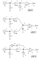
- Figure 1a shows an example of how a disturbing impedance in the form of a stray capacitance affects an electronic circuit.
- the signal source 1 which represents a voltage somewhere in the circuit, is subjected to an equivalent load 2.
- the disturbance source 3 to which the voltage source gives rise generates disturbances in the environment, e.g. at the point 4.
- the disturbances can normally be represented by impedances between the disturbance source and the disturbed point.
- the disturbance is usually capacitive, which is illustrated in Figure 1a by means of the stray capacitance 5.
- the current generated by the capacitive disturbance is added to the current, represented by the current source 6, which normally flows through the disturbed point 4.
- the current is convertible into a voltage 8, which constitutes a measure of the normal signal with the disturbing measuring signal superposed.
- Figure 1b shows an example having more than one disturbing impedance.
- two signal sources 1 and 1' create, with the equivalent loads 2 and 2', two disturbance sources 3 and 3'.
- the figure shows the possibility of different types of disturbing impedances 5 (stray capacitance) and 5' (leak resistance) between the disturbance sources and the disturbed point.
- the normal current to the disturbed point 4 has been assumed to come from a piezoelectric sensor 9.
- Figures 2a and 2b show two known alternative methods for compensating for the existence of the disturbing impedances.
- a signal path including an inverting amplifier 10 and a capacitance 11, has been added parallel to the disturbance.
- the current through the parallel branch can be made to eliminate totally the current through the disturbing impedance.
- the voltage 8 will constitute a direct measure of the normal signal.
- the phase in the compensating branch will be adjusted on the basis of the type of disturbing impedance. This can be realized, for example, by the choice of compensation impedance 11.
- This impedance does not need to be constituted by an actual impedance, but can be constituted by a stray impedance of the same type as the disturbing impedance 5.
- a compensating branch with a different phase can additionally be placed parallel to the signal path represented by 10 and 11. In a number of applications, it is sufficient to make a once-and-for-all adjustment of the amplification at 10, i.e. to use a fixed and passive compensation.
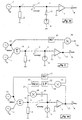
- FIG 3 shows the basic structure of the proposed invention.
- a measuring signal of known characteristics 13 is superposed onto the signal from the normal signal sources of the system. An optimal effect is obtained if the superposition takes place before the signal reaches the region within which the dominant disturbing impedances are found and if the normal signal path is unaffected.
- addition is used in the superposition 14.
- the added measuring signal is affected by the disturbing impedances in similar fashion to the normal signal. This means that, where disturbing impedances exist, there are traces of the measuring signal in the point 15. The size of the disturbing impedances can thus be measured by measuring the measuring-signal content in the point 15.
- the superposed measuring signal 13 is compared to the disturbed signal 15. Where some disturbing impedance is capacitive or inductive, it is necessary to change the relative phase between the signals which are compared in the demodulator 16, for example by 90°. In Figure 3, the superposed measuring signal has been phase-shifted (17).
- the DC-component present in the resultant signal 18 from the demodulator 16 constitutes a measure of the size of the disturbing impedances. Where the normal signal at the point 15 does not have any DC-component, the superposed signal can be constituted by a DC-signal. The extraction of the information concerning the disturbing impedances can then be realized by direct measurement of the DC-component in the point 15.
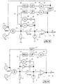
- FIG. 4a, 4b and 4c show three methods for a compensation based upon parallel signal paths.
- a stray capacitance 5 and in Figure 4b a general stray impedance 5" has been assumed.
- the compensation is realized by means of a parallel signal path containing a capacitance 19 and a variable amplifier 20.
- the amplifier can be constituted, for example, by a voltage-controlled amplifier in the form of a multiplier.
- the output signal 18 of the demodulator is connected by means of a low-pass filter 22 and control filter 23 to the control signal 21 for the compensation.
- the setting of the control parameters at the control filter governs the characteristics of the active compensation, e.g. the time constant.
- a simple variant of a control filter includes an integrator and an amplifier.
- control signals are obtained from the output signals of the demodulators using low-pass filtering (22 and 22') and control filtering (23 and 23').
- low-pass filtering 22 and 22'
- control filtering 23 and 23'
- two compensating signal paths are used, which are phase-shifted relative to each other (cartesian compensation). The same effect is achieved where, in addition to the amplitude, adjustment is also made to the phase of a compensating signal path (polar compensation).
- the active compensation in Figure 4a has been supplemented by a passive compensation comprising the capacitor 11 and the fixed amplifier 10.
- a fixed compensation relieves the active compensation, which normally increases the accuracy and reduces the noise.
- the compensation signal has been added in the disturbing point 4. This addition can also be made at a later stage of the (detection) electronics.
- Figures 5a and 5b show two alternative couplings for achieving compensation.
- the circuit designs in these figures contain only those details which relate to the compensation itself. Consideration should naturally be given to how they should be supplemented to ensure that the measurement of the size of the disturbing impedances will be able to be achieved.
- Figure 5a complementary activation for the compensation for a system having a plurality of disturbance sources is used. By varying the relative signal strength of one or more disturbance sources by means of variable amplifiers 24, the disturbing effect caused by the disturbing impedances can be made to cancel each other out. This method normally presupposes that the disturbance sources have different polarity. This is not however necessary where the disturbing impedances comprise both inductances and capacitances.
- complementary detection is used for the compensation in a system having a plurality of disturbed points 4 and 4'.
- complementary detection can be realized by phase-adjustment of the amplifier 26.
- Complementary detection very often affects the normal signal and is expediently used only when the effect upon the normal signal of the superposition in 25 is marginal.
- Figures 5a and 5b can also, of course, be supplemented by fixed compensation according to Figure 4c.
- the information concerning the size of the disturbing impedances is obtained at that frequency/those frequencies which is/are used by the superposed measuring signals.
- the disturbing impedances are only of one type, for example (stray) capacitances
- the use of superposed measuring signals of one frequency is sufficient to achieve effective compensation.
- measuring signals of different frequency may need to be used.
- the compensation is best realized according to the above description where the relative difference between f 0 and the frequency f meas of the superposed measuring signal is small, from experience less than 20%. This guarantees that the setting of the compensation, which is based on f meas , shall also be valid at f 0 .
- a small relative frequency difference is especially crucial where several types of disturbing impedances are of importance. Unless the relative frequency difference can be kept small, and where several types of disturbing impedances are of importance, a plurality of superposed signals of different frequency should be used. Where only one type of disturbing impedance exists, f meas can in certain isolated cases advantageously be chosen at an even multiple of f 0 . The advantage is that the filtering of the demodulated signals then very effectively suppresses the normal frequency f 0 of the system.
- the compensation according to the above description is best realized where a plurality of superposed signals of different frequency are used, especially where different types of disturbing impedances are of importance in the frequency interval which is spanned by f 0 (k) .
- Certain frequency intervals are expediently avoided for the superposed measuring signal. These are constituted by the frequencies in the direct vicinity of odd multiples of f 0 (k) . Where f meas (j) lies in these intervals, the demodulators will react also to the useful signal.
- the width of the unsuitable frequency interval around f 0 (k) is governed by the band width, and hence the time constant, of the low-pass 22 and 22' and control filter filtering 23 and 23'.
- a standard rule of thumb is that the width of the inadmissible intervals should be constituted by a low multiple of the band width of these filters. For certain electrically activated mechanical systems, neither should f meas (j) be chosen closer to the mechanical resonance frequencies than a low multiple of the 3dB-width of the mechanical resonance peaks.
- the superposed measuring signal prefferably has the same characteristics as the normal frequencies of the system, for example as regards the temperature coefficient belonging to the frequency.
- a compensation which is highly stable with respect to temperature and ageing is thereby obtained.
- the superposed signal is generated by an equivalent type of crystal (or LC-oscillator). If the signals have very different characteristics, problems may arise in trying to avoid the above-described inadmissible frequency intervals when the temperature varies and when the system ages.
- the control signals 21 and 21' of the compensation are calculated directly from the output signals from the demodulators 16 and 16'.
- the control signals of the compensation are calculated by weighing up the information from the demodulators measuring the leakage of the superposed measuring signals. This weighing-up procedure means that the number of superposed measuring signals does not need to coincide with the number of correction branches (19-20 and 19'-20' in Figure 4b).
- the vibrating solid-state gyro which is mentioned in the introductory description of the technical problem constitutes an example in which the compensation method which is here proposed can advantageously be used to compensate disturbing impedances between the higher voltages used in activation of the larger amplitude and the small detection currents from the smaller amplitude.
- the compensation method can there be included without the normal signals of the system being affected by the compensation.
- the compensation method offers a necessary reduction and stabilization of the zero-signal, which produces an improved temperature-stability and long-term stability.
- the sensor element for the vibrating solid-state gyro is constituted by a quartz crystal of the tuningfork type, with resonance frequency in the frequency range 27-41 kHz
- the superposed signal is generated, according to this proposal, with a clock crystal as the frequency-determining element (32.8 kHz).
- Clock crystals are cheap and have a fast start time.
- Figure 6a shows an alternative application for the proposed compensation method.
- mechanical resonance frequencies define the frequencies at which the crystal is used. At these frequencies, the phase belonging to the impedance of the crystal has a strong frequency-dependency, which is used to localize the resonance frequencies. Sharpest resonance is achieved where the dielectric capacitance 28 and other disturbing impedances 29 can be disregarded by comparison with that part of the electrical equivalence circuit which describes the mechanical vibration, 28-30.
- C 0 is negligible in relation to QC 1 , in which 1/Q constitutes a measure of the energy losses of the resonator, localization of the resonance frequency is made more difficult by a reduction in the phase variations close to the resonance frequency.
- a difference arises between the electrically measurable and the mechanical resonance frequency.
- An active compensation of C 0 and Z 0 guarantees that the phase condition is fulfilled with respect to resonance, irrespective of temperature and ageing.
- Figure 6b shows an example of a circuit design for the details relating to the actual compensation of C 0 and Z 0 in Figure 6a.
- the circuit design should be supplemented by the superposition of a measuring signal to permit detection of its contribution to the output signal 33 and the production of control signals for the amplifiers in the compensation branches.
- the frequency of the superposed measuring signal does not coincide with some mechanical resonance frequency
- the current through the mechanical equivalence branch 30-32 of the crystal can be neglected.
- the contribution of the superposed measuring signal to the output signal 33 is therefore constituted only by the currents through C 0 , Z 0 and the compensating branches 34-35 and 34'-35', summated by the current-voltage converter 36.
Landscapes
- Physics & Mathematics (AREA)
- General Physics & Mathematics (AREA)
- Noise Elimination (AREA)
- Gyroscopes (AREA)
- Cable Transmission Systems, Equalization Of Radio And Reduction Of Echo (AREA)
- Monitoring And Testing Of Transmission In General (AREA)
- Indication And Recording Devices For Special Purposes And Tariff Metering Devices (AREA)
- Measurement Of Resistance Or Impedance (AREA)
Description
- ... can be used continuously without the normal signal needing to be "shut off".
- ... can be easily applied to an existing circuit design without major modifications.
- ... is suitable for compensation of various types of stray impedances.
- ... that the variation in stray impedances can be tracked by the size of the compensation signals.
- ... does not require external reference signals or reference units.
- ... can be used in any environment whatsoever.
- ... is electronic without moving parts which wear.
- ... is simple and cheap to use.
- Figure 1a
- shows the principle of a system having a stray capacitance,
- Figure 1b
- shows the principle of a piezoelectric system having two different stray impedances and disturbance sources,
- Figure 2a
- shows the principle of a system having a stray capacitance and a passive compensation parallel to the stray capacitance,
- Figure 2b
- shows the principle of a system having a stray capacitance, in which the compensation is realized by means of switching,
- Figure 3
- shows the principle of a system having a stray capacitance, in which a measuring signal has been superposed before the disturbance source,
- Figure 4a
- shows the principle of a system having a stray capacitance, offering a facility for active compensation of the stray capacitance,
- Figure 4b
- shows the principle of a system having a stray impedance, offering a facility for active compensation of two phase components,
- Figure 4c
- shows the principle of a system having a stray capacitance, in which an active compensation has been supplemented by a passive compensation,
- Figure 5a
- shows the principle of a system having two stray capacitances and two disturbance sources, in which the compensation is realized by complementary activation,
- Figure 5b
- shows the principle of a system having two stray capacitances and a disturbance source, in which the compensation is realized by complementary detection,
- Figure 6a
- shows the equivalence circuit for a piezoelectric crystal,
- Figure 6b
- shows the principle of compensation of the dielectric and resistive parts of the equivalence circuit of a piezoelectric crystal.
Claims (5)
- Method for electronically compensating, in an electronic signal-processing system, the electrical disturbance signals which are caused by disturbing impedances and which are appearing superimposed upon the signal that is to be detected, comprising the steps of one or more electrical signals (13) of known characteristics, for example of specific frequencies, being superimposed upon the measuring signal, and the leakage of the superimposed signals (13) as a result of the disturbing impedances being measured, and the result being converted into information (18) which is interpretable by the environment and said information (18) concerning the size of the disturbing impedances and obtained via the superimposed signals (13) being used to compensate actively and continuously for the disturbing impedances via one or more control loops, so that the effect of these disturbing impedances upon the measuring signal is minimized or kept to a predetermined level characterized in that said supplied measuring signals (13) are superimposed upon the normal signal before the region or the points in the system from which the dominating disturbances originate, in that the frequencies of said supplied measuring signals (13) are chosen so that they do not coincide with or lie close to an odd multiple of any one of the characteristic electrical or mechanical frequencies of the system or otherwise adversely affect the normal signal path and functioning of the system, and that said information (18) concerning the size of the disturbing impedances is obtained by comparing the superimposed measuring signals (13) with the measuring signals which have been affected by the disturbing impedances, i e the disturbed signals, (15).
- Method according to claim 1 characterized in that the supplied measuring signals (13) have well-defined frequencies which differ from dominant frequencies in the system by less than 20 % and in that the detection of the superimposed measuring signals (13) is realized by means of phase information.
- Method according to claim 1 characterized in that the active compensation is relieved by being supplemented by a corresponding passive compensation with a fixed amplification, amplitude and phase.
- Method according to claim 1 characterized in that dielectric capacitances (28) in and parallel to a piezoelectric crystal (27) are compensated.
- Method according to claim 1 characterized in that disturbance signals generated by disturbing impedances (15), for example stray capacitances, superimposed upon the output signal of a vibrating solid-state gyro, are compensated.
Applications Claiming Priority (3)
| Application Number | Priority Date | Filing Date | Title |
|---|---|---|---|
| SE9500113 | 1995-01-13 | ||
| SE9500113A SE514499C2 (en) | 1995-01-13 | 1995-01-13 | Method and apparatus for compensating electrical interference |
| PCT/SE1996/000002 WO1996021842A1 (en) | 1995-01-13 | 1996-01-04 | Method and device for electronic compensation of electrical disturbance signals and use thereof |
Publications (2)
| Publication Number | Publication Date |
|---|---|
| EP0803048A1 EP0803048A1 (en) | 1997-10-29 |
| EP0803048B1 true EP0803048B1 (en) | 2001-08-22 |
Family
ID=20396818
Family Applications (1)
| Application Number | Title | Priority Date | Filing Date |
|---|---|---|---|
| EP96900748A Expired - Lifetime EP0803048B1 (en) | 1995-01-13 | 1996-01-04 | Method for electronic compensation of electrical disturbance signals and use thereof |
Country Status (6)
| Country | Link |
|---|---|
| US (1) | US5896033A (en) |
| EP (1) | EP0803048B1 (en) |
| JP (1) | JPH11502015A (en) |
| DE (1) | DE69614664T2 (en) |
| SE (1) | SE514499C2 (en) |
| WO (1) | WO1996021842A1 (en) |
Families Citing this family (4)
| Publication number | Priority date | Publication date | Assignee | Title |
|---|---|---|---|---|
| US7169752B2 (en) * | 2003-09-30 | 2007-01-30 | New River Pharmaceuticals Inc. | Compounds and compositions for prevention of overdose of oxycodone |
| DE10257465B4 (en) * | 2002-12-09 | 2005-03-17 | Siemens Ag | Controllable two-phase network with amplitude compensation |
| FR2942544B1 (en) * | 2009-02-24 | 2015-05-15 | Helion | METHOD FOR CHARACTERIZING AN ELECTRICAL SYSTEM BY SPECTROSCOPY OF IMPEDANCE |
| DE102009031017B4 (en) | 2009-06-29 | 2018-06-21 | Wobben Properties Gmbh | Method and device for monitoring a three-phase alternating voltage network and wind energy plant |
Family Cites Families (9)
| Publication number | Priority date | Publication date | Assignee | Title |
|---|---|---|---|---|
| US3073973A (en) * | 1960-03-04 | 1963-01-15 | Haefely & Cie Ag Emil | Circuit arrangements for the damping of excess voltages in shock potential generators |
| US4288741A (en) * | 1979-05-18 | 1981-09-08 | Auburn International, Inc. | Electrical measurement of fluid void fraction for fluid having capacitive and resistive conductive components |
| DE2932655C2 (en) * | 1979-08-11 | 1982-03-04 | Hewlett-Packard GmbH, 7030 Böblingen | Pulse generator |
| US4377842A (en) * | 1980-10-06 | 1983-03-22 | International Business Machines Corporation | Flyback voltage control |
| JPS5875074A (en) * | 1981-10-30 | 1983-05-06 | Yokogawa Hewlett Packard Ltd | Measuring device for capacity or other parameter |
| US4947130A (en) * | 1987-12-23 | 1990-08-07 | Advantest Corporation | Impedance measuring apparatus |
| SE466817B (en) * | 1989-02-27 | 1992-04-06 | Bofors Ab | BEFORE GYRO PROVIDES SENSOR ELEMENTS |
| US5347870A (en) * | 1992-01-29 | 1994-09-20 | State University Of New York | Dual function system having a piezoelectric element |
| JPH06197294A (en) * | 1992-12-25 | 1994-07-15 | Toshiba Corp | Sample-and-hold circuit |
-
1995
- 1995-01-13 SE SE9500113A patent/SE514499C2/en not_active IP Right Cessation
-
1996
- 1996-01-04 EP EP96900748A patent/EP0803048B1/en not_active Expired - Lifetime
- 1996-01-04 WO PCT/SE1996/000002 patent/WO1996021842A1/en not_active Ceased
- 1996-01-04 US US08/860,794 patent/US5896033A/en not_active Expired - Fee Related
- 1996-01-04 JP JP8521595A patent/JPH11502015A/en active Pending
- 1996-01-04 DE DE69614664T patent/DE69614664T2/en not_active Expired - Fee Related
Also Published As
| Publication number | Publication date |
|---|---|
| SE9500113L (en) | 1996-07-14 |
| SE9500113D0 (en) | 1995-01-13 |
| JPH11502015A (en) | 1999-02-16 |
| DE69614664D1 (en) | 2001-09-27 |
| EP0803048A1 (en) | 1997-10-29 |
| SE514499C2 (en) | 2001-03-05 |
| DE69614664T2 (en) | 2002-07-04 |
| US5896033A (en) | 1999-04-20 |
| WO1996021842A1 (en) | 1996-07-18 |
Similar Documents
| Publication | Publication Date | Title |
|---|---|---|
| US8253426B2 (en) | Capacitance detector | |
| EP2157690B1 (en) | Method, system and apparatus for accurate and stable LC-based reference oscillators | |
| JP3327912B2 (en) | Linear oscillator | |
| RU2483278C2 (en) | Inertial angular velocity sensor with deviation compensation | |
| JPH104318A (en) | Temperature compensated crystal oscillator | |
| US6938462B2 (en) | Device for measuring viscosity and/or density | |
| US20180134544A1 (en) | Temperature compensation for resonant mems | |
| EP0803048B1 (en) | Method for electronic compensation of electrical disturbance signals and use thereof | |
| EP2883307B1 (en) | Method and apparatus to control the lc tank temperature null characteristic in a highly stable lc oscillator | |
| Vyroubal | Eddy-current displacement transducer with extended linear range and automatic tuning | |
| US7839227B2 (en) | Oscillating circuit having an analog oscillating element | |
| US9231520B2 (en) | Wien-bridge oscillator and circuit arrangement for regulating a detuning | |
| JP6352263B2 (en) | Temperature stable LC oscillator and oscillation method with temperature null phase | |
| US6374671B1 (en) | Method of stimulating an oscillator control for capacitive measurement of strength, acceleration and/or rotation speed | |
| JP6191071B2 (en) | Frequency control circuit, oscillation circuit, and oscillator | |
| RU2707394C2 (en) | Generator | |
| JP2850131B2 (en) | Voltage controlled oscillator | |
| Wang et al. | Vibration analysis and control of the quartz rate sensor | |
| Wang et al. | Modeling and Control of the Tuning Fork Gyroscope | |
| JPH07297707A (en) | Phase locked loop oscillator circuit | |
| JPH0640876U (en) | Electrostatic sensor device |
Legal Events
| Date | Code | Title | Description |
|---|---|---|---|
| PUAI | Public reference made under article 153(3) epc to a published international application that has entered the european phase |
Free format text: ORIGINAL CODE: 0009012 |
|
| 17P | Request for examination filed |
Effective date: 19970708 |
|
| AK | Designated contracting states |
Kind code of ref document: A1 Designated state(s): CH DE FR GB IT LI NL |
|
| 17Q | First examination report despatched |
Effective date: 20000509 |
|
| GRAG | Despatch of communication of intention to grant |
Free format text: ORIGINAL CODE: EPIDOS AGRA |
|
| RTI1 | Title (correction) |
Free format text: METHOD FOR ELECTRONIC COMPENSATION OF ELECTRICAL DISTURBANCE SIGNALS AND USE THEREOF |
|
| GRAG | Despatch of communication of intention to grant |
Free format text: ORIGINAL CODE: EPIDOS AGRA |
|
| GRAH | Despatch of communication of intention to grant a patent |
Free format text: ORIGINAL CODE: EPIDOS IGRA |
|
| RIN1 | Information on inventor provided before grant (corrected) |
Inventor name: SOEDERKVIST, JAN |
|
| GRAH | Despatch of communication of intention to grant a patent |
Free format text: ORIGINAL CODE: EPIDOS IGRA |
|
| GRAA | (expected) grant |
Free format text: ORIGINAL CODE: 0009210 |
|
| AK | Designated contracting states |
Kind code of ref document: B1 Designated state(s): CH DE FR GB IT LI NL |
|
| PG25 | Lapsed in a contracting state [announced via postgrant information from national office to epo] |
Ref country code: NL Free format text: LAPSE BECAUSE OF FAILURE TO SUBMIT A TRANSLATION OF THE DESCRIPTION OR TO PAY THE FEE WITHIN THE PRESCRIBED TIME-LIMIT Effective date: 20010822 Ref country code: LI Free format text: LAPSE BECAUSE OF FAILURE TO SUBMIT A TRANSLATION OF THE DESCRIPTION OR TO PAY THE FEE WITHIN THE PRESCRIBED TIME-LIMIT Effective date: 20010822 Ref country code: IT Free format text: LAPSE BECAUSE OF FAILURE TO SUBMIT A TRANSLATION OF THE DESCRIPTION OR TO PAY THE FEE WITHIN THE PRE;WARNING: LAPSES OF ITALIAN PATENTS WITH EFFECTIVE DATE BEFORE 2007 MAY HAVE OCCURRED AT ANY TIME BEFORE 2007. THE CORRECT EFFECTIVE DATE MAY BE DIFFERENT FROM THE ONE RECORDED.SCRIBED TIME-LIMIT Effective date: 20010822 Ref country code: CH Free format text: LAPSE BECAUSE OF FAILURE TO SUBMIT A TRANSLATION OF THE DESCRIPTION OR TO PAY THE FEE WITHIN THE PRESCRIBED TIME-LIMIT Effective date: 20010822 |
|
| REG | Reference to a national code |
Ref country code: CH Ref legal event code: EP |
|
| REF | Corresponds to: |
Ref document number: 69614664 Country of ref document: DE Date of ref document: 20010927 |
|
| ET | Fr: translation filed | ||
| REG | Reference to a national code |
Ref country code: GB Ref legal event code: IF02 |
|
| NLV1 | Nl: lapsed or annulled due to failure to fulfill the requirements of art. 29p and 29m of the patents act | ||
| REG | Reference to a national code |
Ref country code: CH Ref legal event code: PL |
|
| PLBE | No opposition filed within time limit |
Free format text: ORIGINAL CODE: 0009261 |
|
| STAA | Information on the status of an ep patent application or granted ep patent |
Free format text: STATUS: NO OPPOSITION FILED WITHIN TIME LIMIT |
|
| 26N | No opposition filed | ||
| PGFP | Annual fee paid to national office [announced via postgrant information from national office to epo] |
Ref country code: GB Payment date: 20050627 Year of fee payment: 10 |
|
| PGFP | Annual fee paid to national office [announced via postgrant information from national office to epo] |
Ref country code: FR Payment date: 20050704 Year of fee payment: 10 |
|
| PGFP | Annual fee paid to national office [announced via postgrant information from national office to epo] |
Ref country code: DE Payment date: 20050714 Year of fee payment: 10 |
|
| PG25 | Lapsed in a contracting state [announced via postgrant information from national office to epo] |
Ref country code: GB Free format text: LAPSE BECAUSE OF NON-PAYMENT OF DUE FEES Effective date: 20060104 |
|
| PG25 | Lapsed in a contracting state [announced via postgrant information from national office to epo] |
Ref country code: FR Free format text: LAPSE BECAUSE OF NON-PAYMENT OF DUE FEES Effective date: 20060131 |
|
| PG25 | Lapsed in a contracting state [announced via postgrant information from national office to epo] |
Ref country code: DE Free format text: LAPSE BECAUSE OF NON-PAYMENT OF DUE FEES Effective date: 20060801 |
|
| GBPC | Gb: european patent ceased through non-payment of renewal fee |
Effective date: 20060104 |
|
| REG | Reference to a national code |
Ref country code: FR Ref legal event code: ST Effective date: 20060929 |