EP0802568B1 - Semiconductor device - Google Patents
Semiconductor device Download PDFInfo
- Publication number
- EP0802568B1 EP0802568B1 EP96120054A EP96120054A EP0802568B1 EP 0802568 B1 EP0802568 B1 EP 0802568B1 EP 96120054 A EP96120054 A EP 96120054A EP 96120054 A EP96120054 A EP 96120054A EP 0802568 B1 EP0802568 B1 EP 0802568B1
- Authority
- EP
- European Patent Office
- Prior art keywords
- region
- regions
- semiconductor substrate
- primary surface
- conductivity type
- Prior art date
- Legal status (The legal status is an assumption and is not a legal conclusion. Google has not performed a legal analysis and makes no representation as to the accuracy of the status listed.)
- Expired - Lifetime
Links
Images


Classifications
-
- H—ELECTRICITY
- H10—SEMICONDUCTOR DEVICES; ELECTRIC SOLID-STATE DEVICES NOT OTHERWISE PROVIDED FOR
- H10D—INORGANIC ELECTRIC SEMICONDUCTOR DEVICES
- H10D84/00—Integrated devices formed in or on semiconductor substrates that comprise only semiconducting layers, e.g. on Si wafers or on GaAs-on-Si wafers
-
- H—ELECTRICITY
- H10—SEMICONDUCTOR DEVICES; ELECTRIC SOLID-STATE DEVICES NOT OTHERWISE PROVIDED FOR
- H10D—INORGANIC ELECTRIC SEMICONDUCTOR DEVICES
- H10D30/00—Field-effect transistors [FET]
- H10D30/60—Insulated-gate field-effect transistors [IGFET]
- H10D30/64—Double-diffused metal-oxide semiconductor [DMOS] FETs
- H10D30/65—Lateral DMOS [LDMOS] FETs
-
- H—ELECTRICITY
- H10—SEMICONDUCTOR DEVICES; ELECTRIC SOLID-STATE DEVICES NOT OTHERWISE PROVIDED FOR
- H10D—INORGANIC ELECTRIC SEMICONDUCTOR DEVICES
- H10D62/00—Semiconductor bodies, or regions thereof, of devices having potential barriers
- H10D62/10—Shapes, relative sizes or dispositions of the regions of the semiconductor bodies; Shapes of the semiconductor bodies
- H10D62/102—Constructional design considerations for preventing surface leakage or controlling electric field concentration
- H10D62/103—Constructional design considerations for preventing surface leakage or controlling electric field concentration for increasing or controlling the breakdown voltage of reverse-biased devices
- H10D62/105—Constructional design considerations for preventing surface leakage or controlling electric field concentration for increasing or controlling the breakdown voltage of reverse-biased devices by having particular doping profiles, shapes or arrangements of PN junctions; by having supplementary regions, e.g. junction termination extension [JTE]
- H10D62/109—Reduced surface field [RESURF] PN junction structures
-
- H—ELECTRICITY
- H10—SEMICONDUCTOR DEVICES; ELECTRIC SOLID-STATE DEVICES NOT OTHERWISE PROVIDED FOR
- H10D—INORGANIC ELECTRIC SEMICONDUCTOR DEVICES
- H10D62/00—Semiconductor bodies, or regions thereof, of devices having potential barriers
- H10D62/10—Shapes, relative sizes or dispositions of the regions of the semiconductor bodies; Shapes of the semiconductor bodies
- H10D62/13—Semiconductor regions connected to electrodes carrying current to be rectified, amplified or switched, e.g. source or drain regions
- H10D62/149—Source or drain regions of field-effect devices
- H10D62/151—Source or drain regions of field-effect devices of IGFETs
- H10D62/156—Drain regions of DMOS transistors
- H10D62/157—Impurity concentrations or distributions
-
- H—ELECTRICITY
- H10—SEMICONDUCTOR DEVICES; ELECTRIC SOLID-STATE DEVICES NOT OTHERWISE PROVIDED FOR
- H10D—INORGANIC ELECTRIC SEMICONDUCTOR DEVICES
- H10D84/00—Integrated devices formed in or on semiconductor substrates that comprise only semiconducting layers, e.g. on Si wafers or on GaAs-on-Si wafers
- H10D84/80—Integrated devices formed in or on semiconductor substrates that comprise only semiconducting layers, e.g. on Si wafers or on GaAs-on-Si wafers characterised by the integration of at least one component covered by groups H10D12/00 or H10D30/00, e.g. integration of IGFETs
- H10D84/811—Combinations of field-effect devices and one or more diodes, capacitors or resistors
-
- Y—GENERAL TAGGING OF NEW TECHNOLOGICAL DEVELOPMENTS; GENERAL TAGGING OF CROSS-SECTIONAL TECHNOLOGIES SPANNING OVER SEVERAL SECTIONS OF THE IPC; TECHNICAL SUBJECTS COVERED BY FORMER USPC CROSS-REFERENCE ART COLLECTIONS [XRACs] AND DIGESTS
- Y10—TECHNICAL SUBJECTS COVERED BY FORMER USPC
- Y10S—TECHNICAL SUBJECTS COVERED BY FORMER USPC CROSS-REFERENCE ART COLLECTIONS [XRACs] AND DIGESTS
- Y10S257/00—Active solid-state devices, e.g. transistors, solid-state diodes
- Y10S257/90—MOSFET type gate sidewall insulating spacer
Definitions
- the present invention relates to a high voltage semiconductor device having a high breakdown voltage isolation region.
- Figure 12 is a sectional view of a conventional semiconductor device with a level shift function which uses a high breakdown voltage resurf structure and which does not correspond to the device shown in USP 4,292,642.
- the semiconductor device consists of an n-channel resurf MOS FET shown in the left side of the figure, and a resurf isolation island region in the right side of the figure.
- the semiconductor device comprises a p- substrate 1, an n-epitaxial layer 2, a p- diffusion region 3 formed to reach the p- substrate 1, an n+ buried diffusion region 4, an n diffusion region 5, a p diffusion region 6, an oxide film 7, aluminum lead 8, a polysilicon gate 9, an aluminum electrode 10, and a polysilicon 11.
- the aluminum electrode 10 is formed in contact with the n diffusion region 5 and the p diffusion region 6, and has the same potential as that of the resurf isolation island.
- the polysilicon 11 has the same potential as that of the p diffusion region 3, and serves as a field plate.
- the n diffusion region 5 and the n+ buried diffusion region 4 constitute a resurf structure surrounded by the p diffusion region 3.
- the n channel MOS FET is turned on by positively biasing the gate electrode 9. Thereby, a potential difference is caused between the electrode 10 and the aluminum lead 8 by a current flowing through the p diffusion region 6. Outputting this potential difference enables a logic signal applied to the gate 9 to be level shifted to a higher potential.
- a problem in the structure of such conventional high voltage semiconductor devices lie in that, because the aluminum lead 8 at a high potential crosses over the p diffusion region 3 at the substrate potential, a depletion layer is prevented from extending between the n- epitaxial layer 2 and the p diffusion region 3, lowering the breakdown voltage. Countermeasures may be taken to prevent this problem, as shown in Figure 12.
- One approach is to assure the extension of the depletion layer by forming field plates 11 with polysilicon or the like on the pn junction, or to form floating multiple field plates so as to stabilize the surface field with capacitive coupling (see, for example, USP 5,455,439).
- the breakdown voltage is increased, it becomes necessary to considerably thicken an oxide film between the field plates 11 and the aluminum lead 8 to assure dielectric strength of the oxide film itself, thereby increasing the cost to process.
- Document EP-A-0,596,565 discloses a high voltage semiconductor device having a high breakdown voltage isolation region, wherein the level shift of a signal is performed by a MOSFET having a circular arrangement and the level shifted signal is transmitted to the high breakdown voltage isolation region by a conductive layer.
- Is is an object of the invention to provide a high voltage semiconductor device having a high breakdown voltage isolation, wherein the problems described above are eliminated and which can attain a high breakdown voltage isolation with a smaller area and which does not increase the process costs.
- the outer periphery of a region including the second and third regions is surrounded by a region including the first and fifth regions.
- the semiconductor device comprises the first region as an annular first region of a second conductivity type formed on the primary surface of the semiconductor substrate.
- the first region has a relatively low impurity concentration.
- the second region is an annular second region of the second conductivity type formed on the primary surface of the semiconductor substrate in contact with the inside of the first region and has a relatively high impurity concentration.
- the third region of the second conductivity type is formed on the primary surface of the semiconductor substrate with the predetermined spacing to the inside of the second region.
- the third region has a relatively high impurity concentration.
- the conductive layer which holds an insulation layer between the primary surface of the semiconductor substrate, is formed between the second and third regions.
- each depletion layer of the pn junctions which is formed respectively between the second region and the semiconductor substrate and between the third region and the semiconductor substrate, extends to contact each other, before any of the pn junctions reaches a critical field.
- the density of electric force lines at the peripheral corner of each pn junction, which are formed respectively between the second region and the semiconductor substrate and between the third region and the semiconductor substrate, is equal to or less than that of electric force lines on the flat plane of the pn junctions.
- the width of the primary surface of the semiconductor substrate between the second and third regions is formed to be equal to or less than 1.14 times the diffusion depth of the second region.
- the punch through voltage between the second and third regions is formed to be equal to or less than the supply voltage of a control circuit formed on the third regions.
- a field plate is disposed in the insulation layer between the primary surface of the semiconductor substrate and the conductive path, and the field plate is extends over the second and third regions.
- the thickness of the insulation film between the field plate and the third region and the impurity concentration of the third region are adjusted so that breakdown voltage by the insulation layer and the third region is larger than the supply voltage of a control circuit formed on the third region.
- the impurity concentration of the third region is adjusted so that the interface field of the insulation film between the field plate and the third region does not reach the critical field.
- the insulation layer and the impurity concentration of the third region are adjusted so that breakdown voltage by the insulation layer and the third region is larger than the supply voltage of a control circuit formed on the third region.
- the impurity concentration of the third region is adjusted so that the interface field of the insulation layer does not reach the critical field.
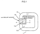
- Figure 1 is a plan view showing the arrangement of semiconductor regions of a semiconductor device according to the first embodiment of the present invention.
- Figure 2 is a cross-sectional view showing the structure taken along the line A-A in the plan view of Figure 1.
- Figure 3 shows equipotential lines in the structure shown in Figure 1.
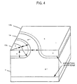
- Figure 4 schematically shows a structure of the corner region of the diffusion regions in the structure of Figure 1.
- Figure 5 shows the result of simulation on the breakdown voltage and punch through voltage in the structure of Figure 4.
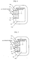
- Figure 6 is a plan view showing the arrangement of semiconductor regions for the semiconductor device according to the second embodiment of the present invention.
- Figure 7 is a plan view showing the arrangement of semiconductor regions for the semiconductor device according to the third embodiment of the present invention.
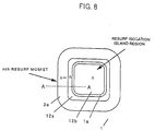
- Figure 8 is a plan view showing the arrangement of semiconductor regions for the semiconductor device according to the fourth embodiment of the present invention.
- Figure 9 is a view showing the cross-sectional structure of a semiconductor device according to the fifth embodiment of the present invention.
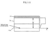
- Figure 10 shows a partial enlarged view of a structure according to the fifth embodiment of the present invention.
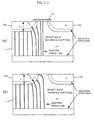
- Figure 11(a) and Figure 11(b) illustrate electric force lines in a region of level shift structure according to the fifth embodiment of the present invention.
- Figure 12 is a sectional view of a conventional semiconductor device with a level shift function.
- Figure 1 is a plan view showing the arrangement of semiconductor regions or a semiconductor device which has a level shift structure according to the first embodiment of the present invention.
- Figure 2 is a cross-sectional view showing the structure taken along the line A-A in the plan view of Figure 1.
- the semiconductor device of the present invention constitutes a resurf structure in which n diffusion regions 12a and 12b are surrounded by n- diffusion regions 2a and 2b, and which is partially divided by a slit.
- the semiconductor device consists of an n channel resurf MOS FET region shown in the left half of the figure and a resurf isolation island region in the right half of the figure.
- the semiconductor device comprises a p- silicon substrate 1 (semiconductor substrate), an n- diffusion region 2a (first region), an n diffusion region 5, a p diffusion region 6 (fourth region), an oxide film 7 (insulation layer), aluminum lead (conductive path) 8, a polysilicon gate 9, an aluminum electrode 10, an n diffusion region 12a (second region), and an n diffusion region 12b (third region). While an n- diffusion region 2b (fifth region) in Figure 1 does not appear in Figure 2, it is formed around the n diffusion region 12b in the same shape as the n- diffusion region 2a.
- the aluminum electrode 10 is formed in contact with the n diffusion region 5 and the p diffusion region 6, and is at the same potential as that of the resurf isolation island.
- the n channel MOS FET is turned on by positively biasing the gate electrode 9. Thereby, a potential difference is caused between the electrode 10 and the aluminum lead 8 by a current flowing through the p diffusion region 6. Outputting this potential difference enables a logic signal applied to the gate 9 to be level shifted to higher potential.
- the structure of the present invention differs from the conventional structure in that there is no resurf structure between the drain of the n channel resurf MOS FET (n diffusion region 12a of Figure 2) and the resurf isolation island region 12b, but the p-substrate region 1 is exposed on the surface with narrow width in the form of a slit-shaped region 1a.
- Figure 3 shows equipotential lines in a case where the n diffusion region 12b is at a high potential in this structure.
- a level shifted signal is output as a potential difference between the electrode 10 and the aluminum lead 8, which is the same potential difference between the n diffusion regions 12a and 12b (i.e. the potential difference between the n diffusion region 12a as the drain of the n channel MOS FET and the resurf isolation island region 12b). Therefore, a punch through voltage between the n diffusion regions 12a and 12b is required to be made higher than the output voltage.
- the output voltage is detected by a control circuit, or the like, having low breakdown voltage included in the resurf isolation island region, the output voltage is designed to be equal to or less than the supply voltage of the control circuit.
- the surface exposed region 1a of the p- substrate 1 should be designed to have a concentration and a distance which is depleted without lowering the resurf breakdown voltage, and which makes the punch through voltage between the n diffusion regions 12a and 12b not less than the supply voltage for the control circuit.
- Figure 4 schematically shows a corner region between the n diffusion regions 12a and 12b in a simplified manner for the analysis. As shown in Figure 4, it is assumed that a pattern corner radius of the n diffusion region 12a is R, and the diffusion depth and lateral diffusion length of the n diffusion regions 12a and 12b is r.
- the pattern corner radius (R), the diffusion depth of n diffusion regions 12a and 12b (r), and the impurity concentration near the surface of p-substrate 1 (Np) are adjusted to satisfy equations (1) and (2).
- the breakdown voltage is generally reduced in comparison to the one-dimensional breakdown voltage between the p-substrate 1 and the n diffusion regions 12a and 12b. This is because electric force lines per unit area at the pn junction corner on the peripheral region of the n diffusion regions 12a and 12b become larger than those on the flat area of the pn junction, so that the electric field at the pn junction corner rises. If the pattern corner radius R of the n diffusion region 12a is sufficiently larger than the diffusion depth and lateral diffusion length r of the n diffusion region 12, the electric field at the pn junction corner is considered to be substantially proportional to: (area of pn junction when viewing from surface)/ (actual area of the pn junction).
- the actual area of the pn junction equals the sum of junction areas of the pn junctions of the n diffusion regions 12a and 12b, while the area of pn junction when viewing from the surface equals the sum of areas of the pn junctions at the corners of n diffusion regions 12a and 12b projected onto a flat plane, and the area on surface of p- substrate 1a (width of 2L) between them.
- width of p- substrate 1 on the surface should be equal to or less than about ( ⁇ - 2) times the diffusion depth (r) of n diffusion regions 12a and 12b.
- the width of p- substrate 1a (2L), the impurity concentration near the surface of p- substrate 1a (Np), and the impurity concentration in the n diffusion regions 12a and 12b near the pn junction (Nn) are adjusted to satisfy the equation (6).
- Figure 5 also shows the result of simulation on the punch through voltage.
- width 2L of the p- substrate 1a at the slit should be designed to be equal to or less than ( ⁇ - 2) times the diffusion depth (r) of n diffusion region 12, that is, to be equal to or less than 1.14 times the depth of the n diffusion region.
- level shift can be attained by forming the n- diffusion region 2a as a level shift element only on one side of the resurf isolation island 12b. Accordingly, the area of device can be significantly reduced. In addition, since there is no need to change the process, there is no increase of process cost.
- Figure 6 is a plan view showing the arrangement of semiconductor regions for the semiconductor device according to the second embodiment of the present invention.
- the cross-sectional structure taken at line A-A in Figure 6 is similar to that in Figure 2, and, therefore, its figure and description are omitted.
- two n- diffusion regions 2a are formed on a p- silicon substrate 1 (semiconductor substrate) separated by a predetermined spacing
- two n diffusion regions 12a are formed respectively in contact with either of the n- diffusion regions 2a, and oppose each other with a predetermined spacing.
- an n diffusion region (third region) 12b is formed with a predetermined spacing to two n diffusion regions (second regions) 12a.
- an n- diffusion region (fourth region) 2b is formed on the periphery of the n diffusion reaion 12b, and opposes the n- diffusion regions 2a (first regions) with a predetermined spacing.
- the reference numerals correspond to the same reference numerals represented in Figures 1 and 2.
- a plurality of small regions 12a are divided from the n resurf isolation island 12b and disposed with spacing, and are separated by each other with spacing. Then, the recion including respective two n diffusion regions (second region) 12a and n diffusion region (third region) 12b is surrounded by a region including the n-diffusion region 2a (first region) and the n- diffusion region 2b (fifth region).
- the second embodiment incorporates two, and generally, a plurality of n channel resurf MOS FETs. With such an arrangement, a plurality of level shift elements can be connected to one resurf isolation island region. Except for such point, functions and effects for isolating high voltage in this semiconductor device are the same as those of the first embodiment shown in Figures 1 and 2. Therefore, a detailed description is omitted here.
- the resurf MOS FETs may be provided only on one side of the resurf isolation island, increase of device area is suppressed.
- Figure 7 is a plan view showing the arrangement of semiconductor regions for the semiconductor device according to the third embodiment of the present invention.
- the cross-sectional structure taken at line A-A in Figure 7 is similar to that in Figure 2, and, therefore, its figure and description are omitted.
- two n- diffusion regions 2a (first regions) separated by a predetermined spacing are formed on a p- silicon substrate 1 (semiconductor substrate), and two n diffusion regions 12a (second regions) are formed in contact with them respectively, and oppose each other with a predetermined spacing.
- An n diffusion region (third region) 12b is formed with a predetermined spacing to two n diffusion regions (second regions) 12a, a portion of which extends between two n diffusion regions (second regions) 12a. Then, an n- diffusion region (fifth region) 2b is formed on the periphery of the n diffusion region 12b, and opposes to the n- diffusion regions 2a (first region) with a predetermined spacing. In addition, the separate portion of the n- diffusion region (fifth region) 2b is disposed between two n- diffusion regions 2a (first regions) with a predetermined spacing between them, continuing from the n diffusion region (third region) 12b between two n diffusion regions (second regions) 12a.
- the semiconductor device of the third embodiment can be considered a plurality of n channel resurf MOS FETs as shown in the device of the first embodiment shown in Figures 1 and 2 and are formed in different locations of one resurf isolation island.
- the third embodiment incorporates a plurality of n channel resurf MOS FETs.
- a difference from the second embodiment lies in that the n- diffusion region 2b is formed in contact with the n diffusion region 12b of the resurf isolation island between two n channel result MOS FETs.
- a plurality of level shift elements can be connected to one resurf isolation island region.
- the resurf MOS FETs are provided only on one side of the resurf isolation island, an increase of device area can be suppressed.
- Figure 7 has two sets of level shift functions by the n channel result MOS FETs, they may be appropriately provided in multiple sets, as required.
- Figure 8 is a plan view showing the arrangement of semiconductor regions for the semiconductor device having a level shift structure according to the fourth embodiment of the present invention.
- the cross-sectional structure at line A-A in Figure 8 is similar to that in Figure 1, and, therefore, its figure and description are omitted.
- an n-diffusion region 2a (first region) is annularly formed on a p- silicon substrate 1 (semiconductor substrate), and an n diffusion region (second region) 12a is annularly formed in contact with the inner periphery of the n-diffusion region 2a.
- an island-shaped n diffusion region 12b is formed with a p- substrate 1a of a predetermined width inbetween.
- the device of the fourth embodiment differs from the first embodiment in that the spacing between the n diffusion regions 12a and 12b is annularly formed, and the n diffusion region 2a is not divided. Except for such point, functions of the device of the fourth embodiment are the same as those shown in Figure 1. Therefore, detailed description is omitted here.
- the structure of the first embodiment shown in Figures 1 and 2 has a possibility of reduction of breakdown voltage because of isolation of the n-diffusion region 2a, the structure of this embodiment has no possibility due to division of the n- diffusion region 2a.
- Figure 9 is a view showing the cross-sectional structure of a semiconductor device having a level shift structure according to the fifth embodiment of the present invention.
- the structure of semiconductor regions of the semiconductor device in a plan view according to the fifth embodiment is the same as Figure 1, therefore, its figure and description are omitted.
- Figure 9 shows a cross-sectional view taken along the line A-A in Figure 1.
- the semiconductor device of the fifth embodiment comprises, as shown by the sectional structure of Figure 9, a p- silicon substrate 1 (semiconductor substrate), an n- diffusion region 2a (first region), an n diffusion region 5, a p diffusion region 6 (fourth region), an oxide film 7 (insulation layer), aluminum lead 8 (conductive path), a polysilicon gate 9, an aluminum electrode 10 formed in contact with the n diffusion region 5 and the p diffusion region 6, and has the same potential as an island potential, an n diffusion region 12a (second region), and an n diffusion region 12b (third region).
- n- diffusion region 2b (fifth region) of Figure 1 is not shown in Figure 9, it is formed on the periphery of the n diffusion region 12b in the same manner as the n-diffusion region 2a. Since these elements are the same as those in Figure 1, a description of the elements is omitted.
- a polysilicon 13 (at the same potential as the n diffusion region 12a of the n channel resurf MOS FET) is disposed in the oxide film 7 so as to cover the region 1a exposed on the surface of the p- substrate 1, holding the underlying oxide film (called an oxide film 7a (insulation film)) therebetween.
- the polysilicon 13 is held at the same potential as the n diffusion region 12a of the n channel resurf MOS FET.
- the polysilicon 13 covers pn junctions formed between the n diffusion regions 12a and 12b, and the p-substrate 1, and extends over the n diffusion regions 12a and 12b.
- Figure 10 shows in a larger scale a structure in which the polysilicon 13 opposes the n diffusion region 12b on the resurf isolation island with the oxide film 7a therebetween. The field distribution is also shown. It is assumed that the thickness of the oxide film 7a under the polysilicon 13 is t, while the thickness of the depletion layer extending into the n diffusion region 12b is d. Breakdown voltage by the silicon oxide film 7a and the n diffusion region 12b must be higher than the supply voltage Vc of the control circuit. Thus, the following equation (7) is obtained. Vc ⁇ q ⁇ Nn ⁇ d/( ⁇ ') ⁇ ( ⁇ ' ⁇ t/ ⁇ ox + d/2)
- the field plate 13 extends to a region where the impurity concentration in the n diffusion region 12b (Nn) is high, as a result, it can be expected that the depletion layer d becomes considerably small.
- the value of first term in the right side of the equation (7) is larger than the control voltage Vc. That is, Vc ⁇ q ⁇ Nn ⁇ d/ ⁇ ') ⁇ ( ⁇ ' ⁇ t/ ⁇ ox)
- Figure 11(a) shows a state of electric force lines in a case where the polysilicon 13 is formed to cover the p- substrate 1a as shown in Figure 9, in comparison with Figure 11 (b) where there is no polysilicon 13.
- parts of the electric force lines terminate on the polysilicon 13 because the polysilicon 13 is over the surface region of p- substrate 1a, so that the electric field is relaxed at the pn junction corner. This further prevents the breakdown voltage between the p- substrate 1 and the n diffusion region 12a and 12b from being reduced.
- Figure 5 also shows the result of simulation on the breakdown voltage when the field plate 13 exists. It is 85% of one-dimensional breakdown voltage, and the breakdown voltage is improved by 6% over the case where there is no field plate. With this arrangement, it is possible to further improve the breakdown voltage and the punch through voltage in addition to the advantages of the first embodiment.
- the device of Figure 9 is an example in which a field plate 13 is added to the device of the first embodiment shown in Figures 1 and 2.
- the field plate is also applicable to the devices of the second through fourth embodiments shown in Figures 6 through 8.
- the above analysis is directed to the polysilicon 13 disposed in the oxide film 7, the oxide film 7a and the n diffusion region 12b thereunder.
- the same analysis is applied to the breakdown voltage of the aluminum lead 8, the oxide film 7 and the n diffusion region 12b in the devices of the first through fourth embodiments shown in Figures 1 through 8. That is, in these cases, the thickness of oxide film (t) just under the aluminum lead 8 and the impurity concentration of the n diffusion region 12b (Nn) are adjusted to satisfy the conditions of equations 7 through 9.
- the present invention can provide a semiconductor device having a high voltage isolation region between a low breakdown voltage region and a high breakdown voltage region, and has a level shift function to the high breakdown voltage region.
- the high voltage semiconductor device according to the present invention can be obtained within a small area and without increasing the process cost.
Landscapes
- Insulated Gate Type Field-Effect Transistor (AREA)
- Metal-Oxide And Bipolar Metal-Oxide Semiconductor Integrated Circuits (AREA)
- Element Separation (AREA)
Description
- The present invention relates to a high voltage semiconductor device having a high breakdown voltage isolation region.
- There is known a conventional high voltage semiconductor devices which includes a high breakdown voltage isolation region using a resurf structure (see, for example, USP 4,292,642). Figure 12 is a sectional view of a conventional semiconductor device with a level shift function which uses a high breakdown voltage resurf structure and which does not correspond to the device shown in USP 4,292,642. As shown in the figure, the semiconductor device consists of an n-channel resurf MOS FET shown in the left side of the figure, and a resurf isolation island region in the right side of the figure. The semiconductor device comprises a p-
substrate 1, an n-epitaxial layer 2, a p-diffusion region 3 formed to reach the p-substrate 1, an n+ buried diffusion region 4, ann diffusion region 5,a p diffusion region 6, anoxide film 7,aluminum lead 8, apolysilicon gate 9, analuminum electrode 10, and a polysilicon 11. Thealuminum electrode 10 is formed in contact with then diffusion region 5 and thep diffusion region 6, and has the same potential as that of the resurf isolation island. The polysilicon 11 has the same potential as that of thep diffusion region 3, and serves as a field plate. In addition, then diffusion region 5 and the n+ buried diffusion region 4 constitute a resurf structure surrounded by thep diffusion region 3. - In the semiconductor device arranged as above, the n channel MOS FET is turned on by positively biasing the
gate electrode 9. Thereby, a potential difference is caused between theelectrode 10 and thealuminum lead 8 by a current flowing through thep diffusion region 6. Outputting this potential difference enables a logic signal applied to thegate 9 to be level shifted to a higher potential. - A problem in the structure of such conventional high voltage semiconductor devices lie in that, because the aluminum lead 8 at a high potential crosses over the
p diffusion region 3 at the substrate potential, a depletion layer is prevented from extending between the n-epitaxial layer 2 and thep diffusion region 3, lowering the breakdown voltage. Countermeasures may be taken to prevent this problem, as shown in Figure 12. One approach is to assure the extension of the depletion layer by forming field plates 11 with polysilicon or the like on the pn junction, or to form floating multiple field plates so as to stabilize the surface field with capacitive coupling (see, for example, USP 5,455,439). However, such approach has a problem. As the breakdown voltage is increased, it becomes necessary to considerably thicken an oxide film between the field plates 11 and thealuminum lead 8 to assure dielectric strength of the oxide film itself, thereby increasing the cost to process. - Document EP-A-0,409,746 discloses a semiconductor device comprising
- a semiconductor substrate of a first conductivity type,
- a first region of a second conductivity type formed on the primary surface of the semiconductor substrate and having a relatively low impurity concentration,
- a second region of the second conductivity type formed on the primary surface of the semiconductor substrate in contact with the first region and having a relatively high impurity concentration,
- a third region of the second conductivity type formed on the primary surface of the semiconductor substrate with a predetermined spacing to said second region and having a relatively high impurity concentration,
- a fourth region of the second conductivity type formed on the primary surface of the semiconductor substrate in contact with the third region and with a predetermined spacing to said first region and having a relatively low impurity concentration, and
- at least one conductive layer formed over the primary surface of the semiconductor substrate with an insulation layer in between and connecting said second region and said third region. The conductive layer is connected to a gate electrode 63 of a MOSFET.
-
- Document EP-A-0,596,565 discloses a high voltage semiconductor device having a high breakdown voltage isolation region, wherein the level shift of a signal is performed by a MOSFET having a circular arrangement and the level shifted signal is transmitted to the high breakdown voltage isolation region by a conductive layer.
- Is is an object of the invention to provide a high voltage semiconductor device having a high breakdown voltage isolation, wherein the problems described above are eliminated and which can attain a high breakdown voltage isolation with a smaller area and which does not increase the process costs.
- This object is achieved by a semiconductor device according to
claim - Further developments of the invention are given in the dependent claims.
- In another aspect of the invention, in the semiconductor device as set forth above, the outer periphery of a region including the second and third regions is surrounded by a region including the first and fifth regions.
- According to an aspect of the present invention, the semiconductor device comprises the first region as an annular first region of a second conductivity type formed on the primary surface of the semiconductor substrate. The first region has a relatively low impurity concentration. The second region is an annular second region of the second conductivity type formed on the primary surface of the semiconductor substrate in contact with the inside of the first region and has a relatively high impurity concentration. The third region of the second conductivity type is formed on the primary surface of the semiconductor substrate with the predetermined spacing to the inside of the second region. The third region has a relatively high impurity concentration. The conductive layer, which holds an insulation layer between the primary surface of the semiconductor substrate, is formed between the second and third regions.
- In another aspect of the invention, each depletion layer of the pn junctions, which is formed respectively between the second region and the semiconductor substrate and between the third region and the semiconductor substrate, extends to contact each other, before any of the pn junctions reaches a critical field.
- In another aspect of the invention, the density of electric force lines at the peripheral corner of each pn junction, which are formed respectively between the second region and the semiconductor substrate and between the third region and the semiconductor substrate, is equal to or less than that of electric force lines on the flat plane of the pn junctions.
- In another aspect of the invention, the width of the primary surface of the semiconductor substrate between the second and third regions is formed to be equal to or less than 1.14 times the diffusion depth of the second region.
- In another aspect of the invention, the punch through voltage between the second and third regions is formed to be equal to or less than the supply voltage of a control circuit formed on the third regions.
- In another aspect of the invention, a field plate is disposed in the insulation layer between the primary surface of the semiconductor substrate and the conductive path, and the field plate is extends over the second and third regions.
- In another aspect of the invention, the thickness of the insulation film between the field plate and the third region and the impurity concentration of the third region, are adjusted so that breakdown voltage by the insulation layer and the third region is larger than the supply voltage of a control circuit formed on the third region.
- In another aspect of the invention, the impurity concentration of the third region is adjusted so that the interface field of the insulation film between the field plate and the third region does not reach the critical field.
- In another aspect of the invention, the insulation layer and the impurity concentration of the third region are adjusted so that breakdown voltage by the insulation layer and the third region is larger than the supply voltage of a control circuit formed on the third region.
- In another aspect of the invention, the impurity concentration of the third region is adjusted so that the interface field of the insulation layer does not reach the critical field.
- Other features and advantages of the invention will be apparent from the following description.
- Figure 1 is a plan view showing the arrangement of semiconductor regions of a semiconductor device according to the first embodiment of the present invention.
- Figure 2 is a cross-sectional view showing the structure taken along the line A-A in the plan view of Figure 1.
- Figure 3 shows equipotential lines in the structure shown in Figure 1.
- Figure 4 schematically shows a structure of the corner region of the diffusion regions in the structure of Figure 1.
- Figure 5 shows the result of simulation on the breakdown voltage and punch through voltage in the structure of Figure 4.
- Figure 6 is a plan view showing the arrangement of semiconductor regions for the semiconductor device according to the second embodiment of the present invention.
- Figure 7 is a plan view showing the arrangement of semiconductor regions for the semiconductor device according to the third embodiment of the present invention.
- Figure 8 is a plan view showing the arrangement of semiconductor regions for the semiconductor device according to the fourth embodiment of the present invention.
- Figure 9 is a view showing the cross-sectional structure of a semiconductor device according to the fifth embodiment of the present invention.
- Figure 10 shows a partial enlarged view of a structure according to the fifth embodiment of the present invention.
- Figure 11(a) and Figure 11(b) illustrate electric force lines in a region of level shift structure according to the fifth embodiment of the present invention.
- Figure 12 is a sectional view of a conventional semiconductor device with a level shift function.
- Figure 1 is a plan view showing the arrangement of semiconductor regions or a semiconductor device which has a level shift structure according to the first embodiment of the present invention. Figure 2 is a cross-sectional view showing the structure taken along the line A-A in the plan view of Figure 1.
- First, as shown in the plan view of Figure 1, the semiconductor device of the present invention constitutes a resurf structure in which
n diffusion regions diffusion regions diffusion region 2a (first region), ann diffusion region 5, a p diffusion region 6 (fourth region), an oxide film 7 (insulation layer), aluminum lead (conductive path) 8, apolysilicon gate 9, analuminum electrode 10, ann diffusion region 12a (second region), and ann diffusion region 12b (third region). While an n-diffusion region 2b (fifth region) in Figure 1 does not appear in Figure 2, it is formed around then diffusion region 12b in the same shape as the n-diffusion region 2a. In addition, thealuminum electrode 10 is formed in contact with then diffusion region 5 and thep diffusion region 6, and is at the same potential as that of the resurf isolation island. - In the semiconductor device constituted as above, the n channel MOS FET is turned on by positively biasing the
gate electrode 9. Thereby, a potential difference is caused between theelectrode 10 and thealuminum lead 8 by a current flowing through thep diffusion region 6. Outputting this potential difference enables a logic signal applied to thegate 9 to be level shifted to higher potential. - The structure of the present invention differs from the conventional structure in that there is no resurf structure between the drain of the n channel resurf MOS FET (
n diffusion region 12a of Figure 2) and the resurfisolation island region 12b, but the p-substrate region 1 is exposed on the surface with narrow width in the form of a slit-shaped region 1a. - Figure 3 shows equipotential lines in a case where the
n diffusion region 12b is at a high potential in this structure. - As shown in Figure 3, since the p- substrate region 1a positioned between the
n diffusion regions n diffusion regions aluminum lead 8 and the surface of thesubstrate silicon 1, eliminating the prior art problem of field concentration. - Further, a level shifted signal is output as a potential difference between the
electrode 10 and thealuminum lead 8, which is the same potential difference between then diffusion regions n diffusion region 12a as the drain of the n channel MOS FET and the resurfisolation island region 12b). Therefore, a punch through voltage between then diffusion regions - From the above, the surface exposed region 1a of the p-
substrate 1 should be designed to have a concentration and a distance which is depleted without lowering the resurf breakdown voltage, and which makes the punch through voltage between then diffusion regions - This is analytically discussed. Figure 4 schematically shows a corner region between the
n diffusion regions n diffusion region 12a is R, and the diffusion depth and lateral diffusion length of then diffusion regions - A necessary condition, not affecting the resurf breakdown voltage, is that the pn junction field does not reach the critical field when the depletion layers extending from the
n diffusion regions n diffusion regions - Ecr: Critical field (about 2.5E5 V/cm)
- E1: Pn junction field when depletion layers contact at the center
- q: Amount of charge of electron
- Np: Impurity concentration near surface of p-
substrate 1 - ε: Dielectric constant of vacuum
- ε': Specific dielectric constant of silicon
-
- If R » r, it is approximated by the following equation:
- Therefore, the pattern corner radius (R), the diffusion depth of
n diffusion regions - Next, when the structure of Figure 4 is employed, the breakdown voltage is generally reduced in comparison to the one-dimensional breakdown voltage between the p-
substrate 1 and then diffusion regions n diffusion regions n diffusion region 12a is sufficiently larger than the diffusion depth and lateral diffusion length r of then diffusion region 12, the electric field at the pn junction corner is considered to be substantially proportional to:n diffusion regions n diffusion regions - Therefore, it is sufficient to design this value to be equal to or less than 1, that is, the electric field at the pn junction corner should be equal to or less than that on the flat area of pn junction. This condition is expressed by equation (3)
- If R » r, then
- It is found that the width of p-
substrate 1 on the surface (width of slit-shaped p- substrate 1a (2L)) should be equal to or less than about (π - 2) times the diffusion depth (r) ofn diffusion regions - The result of this analysis confirmed by two-dimensional simulation for R » r is shown in Figure 5. As seen from the figure, when width 2L on the surface of p-
substrate 1 becomes larger than about (π - 2) times the diffusion depth (r) ofn diffusion region 12, the breakdown voltage at the corner of the pn junction becomes less than 80% of the one-dimensional breakdown voltage. In addition, it is found that, when L is sufficiently large (2L = ∞), the breakdown voltage is reduced to 43% of the one-dimensional breakdown voltage. - Then, from the above discussion, the punch through voltage V between the
n diffusion regions - q: Amount of charge of electron
- Nn: Impurity concentration in
n diffusion regions - Np: Impurity concentration near the surface of p-
substrate 1 - ε : Dielectric constant of vacuum
- ε' : Specific dielectric constant of silicon
-
- Therefore, the width of p- substrate 1a (2L), the impurity concentration near the surface of p- substrate 1a (Np), and the impurity concentration in the
n diffusion regions - Figure 5 also shows the result of simulation on the punch through voltage. When the width on the surface of p- substrate 1 (2L) is (π - 2) times the diffusion depth (r) of
n diffusion regions n diffusion region 12, that is, to be equal to or less than 1.14 times the depth of the n diffusion region. - With the structure of the semiconductor device according to this embodiment, level shift can be attained by forming the n-
diffusion region 2a as a level shift element only on one side of theresurf isolation island 12b. Accordingly, the area of device can be significantly reduced. In addition, since there is no need to change the process, there is no increase of process cost. - Figure 6 is a plan view showing the arrangement of semiconductor regions for the semiconductor device according to the second embodiment of the present invention. The cross-sectional structure taken at line A-A in Figure 6 is similar to that in Figure 2, and, therefore, its figure and description are omitted. In the semiconductor device of the second embodiment, as shown by the plan view of Figure 6, two n-
diffusion regions 2a (first regions) are formed on a p- silicon substrate 1 (semiconductor substrate) separated by a predetermined spacing, and twon diffusion regions 12a (second regions) are formed respectively in contact with either of the n-diffusion regions 2a, and oppose each other with a predetermined spacing. In addition, an n diffusion region (third region) 12b is formed with a predetermined spacing to two n diffusion regions (second regions) 12a. Then, an n- diffusion region (fourth region) 2b is formed on the periphery of then diffusion reaion 12b, and opposes the n-diffusion regions 2a (first regions) with a predetermined spacing. In the figure, the reference numerals correspond to the same reference numerals represented in Figures 1 and 2. - In the structure of the second embodiment as stated above, a plurality of
small regions 12a are divided from the nresurf isolation island 12b and disposed with spacing, and are separated by each other with spacing. Then, the recion including respective two n diffusion regions (second region) 12a and n diffusion region (third region) 12b is surrounded by a region including the n-diffusion region 2a (first region) and the n-diffusion region 2b (fifth region). - As described, the second embodiment incorporates two, and generally, a plurality of n channel resurf MOS FETs. With such an arrangement, a plurality of level shift elements can be connected to one resurf isolation island region. Except for such point, functions and effects for isolating high voltage in this semiconductor device are the same as those of the first embodiment shown in Figures 1 and 2. Therefore, a detailed description is omitted here. In the structure of this second embodiment, since the resurf MOS FETs may be provided only on one side of the resurf isolation island, increase of device area is suppressed.
- Figure 7 is a plan view showing the arrangement of semiconductor regions for the semiconductor device according to the third embodiment of the present invention. The cross-sectional structure taken at line A-A in Figure 7 is similar to that in Figure 2, and, therefore, its figure and description are omitted. In the semiconductor device of the third embodiment, as shown by the plan view of Figure 7, two n-
diffusion regions 2a (first regions) separated by a predetermined spacing are formed on a p- silicon substrate 1 (semiconductor substrate), and twon diffusion regions 12a (second regions) are formed in contact with them respectively, and oppose each other with a predetermined spacing. An n diffusion region (third region) 12b is formed with a predetermined spacing to two n diffusion regions (second regions) 12a, a portion of which extends between two n diffusion regions (second regions) 12a. Then, an n- diffusion region (fifth region) 2b is formed on the periphery of then diffusion region 12b, and opposes to the n-diffusion regions 2a (first region) with a predetermined spacing. In addition, the separate portion of the n- diffusion region (fifth region) 2b is disposed between two n-diffusion regions 2a (first regions) with a predetermined spacing between them, continuing from the n diffusion region (third region) 12b between two n diffusion regions (second regions) 12a. - The semiconductor device of the third embodiment can be considered a plurality of n channel resurf MOS FETs as shown in the device of the first embodiment shown in Figures 1 and 2 and are formed in different locations of one resurf isolation island.
- Thus, the third embodiment incorporates a plurality of n channel resurf MOS FETs. A difference from the second embodiment lies in that the n-
diffusion region 2b is formed in contact with then diffusion region 12b of the resurf isolation island between two n channel result MOS FETs. With such an arrangement, a plurality of level shift elements can be connected to one resurf isolation island region. In addition, since the resurf MOS FETs are provided only on one side of the resurf isolation island, an increase of device area can be suppressed. Furthermore, it is possible to prevent parasitic operations caused by a parasitic element L-npn (lateral transistor structure) between two n channel resurf MOS FETs. - While the example of Figure 7 has two sets of level shift functions by the n channel result MOS FETs, they may be appropriately provided in multiple sets, as required.
- Figure 8 is a plan view showing the arrangement of semiconductor regions for the semiconductor device having a level shift structure according to the fourth embodiment of the present invention. The cross-sectional structure at line A-A in Figure 8 is similar to that in Figure 1, and, therefore, its figure and description are omitted.
- In the semiconductor device of the fourth embodiment, as shown in the plan view of Figure 8, an n-
diffusion region 2a (first region) is annularly formed on a p- silicon substrate 1 (semiconductor substrate), and an n diffusion region (second region) 12a is annularly formed in contact with the inner periphery of the n-diffusion region 2a. In addition, in the inside of then diffusion region 12a, an island-shapedn diffusion region 12b is formed with a p- substrate 1a of a predetermined width inbetween. - Thus, the device of the fourth embodiment differs from the first embodiment in that the spacing between the
n diffusion regions n diffusion region 2a is not divided. Except for such point, functions of the device of the fourth embodiment are the same as those shown in Figure 1. Therefore, detailed description is omitted here. Although the structure of the first embodiment shown in Figures 1 and 2 has a possibility of reduction of breakdown voltage because of isolation of the n-diffusion region 2a, the structure of this embodiment has no possibility due to division of the n-diffusion region 2a. - Figure 9 is a view showing the cross-sectional structure of a semiconductor device having a level shift structure according to the fifth embodiment of the present invention. The structure of semiconductor regions of the semiconductor device in a plan view according to the fifth embodiment is the same as Figure 1, therefore, its figure and description are omitted. Figure 9 shows a cross-sectional view taken along the line A-A in Figure 1. The semiconductor device of the fifth embodiment comprises, as shown by the sectional structure of Figure 9, a p- silicon substrate 1 (semiconductor substrate), an n-
diffusion region 2a (first region), ann diffusion region 5, a p diffusion region 6 (fourth region), an oxide film 7 (insulation layer), aluminum lead 8 (conductive path), apolysilicon gate 9, analuminum electrode 10 formed in contact with then diffusion region 5 and thep diffusion region 6, and has the same potential as an island potential, ann diffusion region 12a (second region), and ann diffusion region 12b (third region). In addition, although the n-diffusion region 2b (fifth region) of Figure 1 is not shown in Figure 9, it is formed on the periphery of then diffusion region 12b in the same manner as the n-diffusion region 2a. Since these elements are the same as those in Figure 1, a description of the elements is omitted. - Further, in the fifth embodiment, in addition to the structure of the first embodiment, a polysilicon 13 (at the same potential as the
n diffusion region 12a of the n channel resurf MOS FET) is disposed in theoxide film 7 so as to cover the region 1a exposed on the surface of the p-substrate 1, holding the underlying oxide film (called an oxide film 7a (insulation film)) therebetween. Thepolysilicon 13 is held at the same potential as then diffusion region 12a of the n channel resurf MOS FET. Then, thepolysilicon 13 covers pn junctions formed between then diffusion regions substrate 1, and extends over then diffusion regions n diffusion regions n diffusion region 12a of the n channel MOS drain and then diffusion region 12b of the resurf isolation island can be prevented by a field plate effect of thepolysilicon layer 13. - However, if the oxide film 7a under the
polysilicon 13 is too thin, field concentration may occur on the Si surface under thepolysilicon 13 so that the breakdown voltage may be reduced. Therefore, the following conditions should be satisfied. First, Figure 10 shows in a larger scale a structure in which thepolysilicon 13 opposes then diffusion region 12b on the resurf isolation island with the oxide film 7a therebetween. The field distribution is also shown. It is assumed that the thickness of the oxide film 7a under thepolysilicon 13 is t, while the thickness of the depletion layer extending into then diffusion region 12b is d. Breakdown voltage by the silicon oxide film 7a and then diffusion region 12b must be higher than the supply voltage Vc of the control circuit. Thus, the following equation (7) is obtained. - In addition, since the electrical field at the interface of silicon oxide film 7a must be the critical voltage Ecr' or lower, the following equation (8) is obtained.
- In these equations,
- Ecr': Critical field at the interface of silicon and silicon oxide film (about 5E5 V/cm)
- q: Amount of charge of electron
- Nn: Impurity concentration in
n diffusion region 12b - ε: Dielectric constant of vacuum
- ε': Specific dielectric constant of silicon
- ε ox: Specific dielectric constant of oxide film
- d: Width of depletion layer just under end of
polysilicon 13 - t: Thickness of oxide film just under end of
polysilicon 13 -
- In most cases, the
field plate 13 extends to a region where the impurity concentration in then diffusion region 12b (Nn) is high, as a result, it can be expected that the depletion layer d becomes considerably small. Thus, it is generally desirable that the value of first term in the right side of the equation (7) is larger than the control voltage Vc. That is, - Thus,
- The thickness of the oxide film just under the end of polysilicon 13 (t) and the impurity concentration in the
n diffusion region 12b (Nn) are adjusted to satisfy equations (7) - (9). - In addition, Figure 11(a) shows a state of electric force lines in a case where the
polysilicon 13 is formed to cover the p- substrate 1a as shown in Figure 9, in comparison with Figure 11 (b) where there is nopolysilicon 13. As shown in Figure 11(a), parts of the electric force lines terminate on thepolysilicon 13 because thepolysilicon 13 is over the surface region of p- substrate 1a, so that the electric field is relaxed at the pn junction corner. This further prevents the breakdown voltage between the p-substrate 1 and then diffusion region - Figure 5 also shows the result of simulation on the breakdown voltage when the
field plate 13 exists. It is 85% of one-dimensional breakdown voltage, and the breakdown voltage is improved by 6% over the case where there is no field plate. With this arrangement, it is possible to further improve the breakdown voltage and the punch through voltage in addition to the advantages of the first embodiment. - Furthermore, the device of Figure 9 is an example in which a
field plate 13 is added to the device of the first embodiment shown in Figures 1 and 2. The field plate is also applicable to the devices of the second through fourth embodiments shown in Figures 6 through 8. - The above analysis is directed to the
polysilicon 13 disposed in theoxide film 7, the oxide film 7a and then diffusion region 12b thereunder. The same analysis is applied to the breakdown voltage of thealuminum lead 8, theoxide film 7 and then diffusion region 12b in the devices of the first through fourth embodiments shown in Figures 1 through 8. That is, in these cases, the thickness of oxide film (t) just under thealuminum lead 8 and the impurity concentration of then diffusion region 12b (Nn) are adjusted to satisfy the conditions ofequations 7 through 9. - As described above, the present invention can provide a semiconductor device having a high voltage isolation region between a low breakdown voltage region and a high breakdown voltage region, and has a level shift function to the high breakdown voltage region. The high voltage semiconductor device according to the present invention can be obtained within a small area and without increasing the process cost.
Claims (10)
- A high voltage semiconductor device having a high breakdown voltage isolation, comprising:whereby a logic signal applied to said gate electrode (9) as a potential difference relative to a first potential is output as a level shifted logic signal between said fourth region (6) and said third region (12b) as a potential difference relative to a second potential higher than said first potential.a semiconductor substrate (1) of a first conductivity type;a MOS field effect transistor including a gate electrode (9) and two source/drain regions (5, 2a, 12a), wherein one of said source/drain regions comprisesa first region (2a) having a second conductivity type, formed on the primary surface of said semiconductor substrate (1), and having a relatively low impurity concentration, anda second region (12a) having the second conductivity type, formed on the primary surface of said semiconductor substrate (1) in contact with said first region (2a), and having a relatively high impurity concentration;a third region (12b) having the second conductivity type, formed on the primary surface of said semiconductor substrate (1) with a first predetermined spacing to said second region (12a), and having a relatively high impurity concentration, the first predetermined spacing being provided by a portion (1a) of said semiconductor substrate (1) and having a relatively low impurity concentration said first spacing predetermined for securing the high breakdown voltage;a fourth region (6) having the first conductivity type formed in said third region (12b);a fifth region (2b) having the second conductivity type, formed on the primary surface of said semiconductor substrate (1) in contact with said third region (12b) and with a second predetermined spacing to said first region (2a) and having a relatively low impurity concentration, the second predetermined spacing being provided by a portion (1a) of said semiconductor substrate (1); andat least one conductive layer (8) formed over the primary surface of said semiconductor substrate (1) with an insulation layer (7) inbetween, and electrically connecting said second region (12a) and said fourth region (6),
- The semiconductor device according to claim 1, characterized in thata plurality of said MOS field effect transistors is formed, each comprising a first region (2a) having the second conductivity type formed on the primary surface of said semiconductor substrate (1) and a second region (12a) having the second conductivity type formed on the primary surface of said semiconductor substrate (1) in contact with a respective one of said plurality of first regions (2a);said third region (12b) is formed on the primary surface of said semiconductor substrate with a predetermined spacing to said plurality of respective second regions (12a);said fifth region (2b) is formed on the primary surface of said semiconductor substrate (1) in contact with said third region (12b) and is formed with a predetermined spacing to said plurality of respective first regions (2a); anda plurality of said conductive layers (8) is formed over the primary surface of said semiconductor substrate (1) via said insulation layer (7), each connecting a respective one of said plurality of second regions (12a) and said fourth region (6).
- The semiconductor device according to claim 2, characterized in thatsaid third region (12b) has a region held between two adjacent of said plurality of second regions (12a) and formed with a predetermined spacing to said respective second regions (12a); andsaid fifth region (2b) has a region disposed between two adjacent of said plurality of first regions (2a) and in contact with said region of said third region (12b), the region being formed with a predetermined spacing to said plurality of first regions (2a).
- The semiconductor device according to claim 2, characterized in thatsaid plurality of first regions (2a) is formed with a predetermined spacing to each other; andsaid plurality of second regions is formed with a predetermined spacing to each other.
- A semiconductor device as set forth in any one of claims 1 to 4, characterized in that
the outer periphery of a region including said second and third regions (12a), (12b) is surrounded by a region including said first and fifth regions (2a), (2b). - A high voltage semiconductor device having a high breakdown voltage isolation, comprising:whereby a logic signal applied to gate electrode (9) as a potential difference relative to a first potential is output as a level shifted logic signal between said fourth region (6) and said third region (12b) as a potential difference relative to a second potential higher than said first potential.a semiconductor substrate (1) of a first conductivity type;a MOS field effect transistor including a gate electrode (9) and two source/drain regions (5, 2a, 12a), wherein one of said source/drain regions comprisesan annular first region (2a) having a second conductivity type formed on the primary surface of said semiconductor substrate (1), and having a relatively low impurity concentration, andan annular second region (12a) having the second conductivity type formed on the primary surface of said semiconductor substrate (1) in contact with the inside of said first region (2a), and having a relatively high impurity concentration;a third region (12b) having the second conductivity type formed on the primary surface of said semiconductor substrate (1) with a predetermined spacing to the inside of said second region (12a), and having a relatively high impurity concentration, the predetermined spacing being provided by a portion (1a) of said semiconductor substrate (1) and having a relatively low impurity concentration, said spacing predetermined for securing the high breakdown voltage;a fourth region (6) having the first conductivity type formed in said third region (12b); andat least one conductive layer (8) formed over the primary surface of said semiconductor substrate (1) with an insulation layer (7) inbetween, and electrically connecting said second region (12a) and said fourth region (6),
- The semiconductor device as set forth in any one of claims 1 through 6, characterized in that
the width of primary surface of said semiconductor substrate (1) between said second and third regions (12a), (12b) is formed to be equal to or less than 1.14 times the diffusion depth of the second region (12a). - The semiconductor device as set forth in any one of claims 1 through 7, characterized in that
a field plate (13) is disposed in said insulation layer (7) between the primary surface of said semiconductor substrate and said conductive layer (8), said field plate (13) is extending over said second and third regions (12a), (12b). - The semiconductor device as set forth in claim 8, characterized in that
the thickness of the insulation film (7a) between said field plate (13) and said third region (12b) and the impurity concentration of said third region (12b) are adjusted so that breakdown voltage between said insulation layer (7a) and said third region (12b) is larger than the supply voltage of a control circuit formed on said third region (12b). - The semiconductor device as set forth in any one of claims 1 through 9, characterized in that
said insulation layer (7) and the impurity concentration of said third region (12b) are adjusted so that breakdown voltage between said insulation layer (7) and said third region (12b) is larger than the supply voltage of a control circuit formed on said third region (12b).
Applications Claiming Priority (3)
| Application Number | Priority Date | Filing Date | Title |
|---|---|---|---|
| JP09224096A JP3917211B2 (en) | 1996-04-15 | 1996-04-15 | Semiconductor device |
| JP92240/96 | 1996-04-15 | ||
| JP9224096 | 1996-04-15 |
Publications (2)
| Publication Number | Publication Date |
|---|---|
| EP0802568A1 EP0802568A1 (en) | 1997-10-22 |
| EP0802568B1 true EP0802568B1 (en) | 2002-03-27 |
Family
ID=14048919
Family Applications (1)
| Application Number | Title | Priority Date | Filing Date |
|---|---|---|---|
| EP96120054A Expired - Lifetime EP0802568B1 (en) | 1996-04-15 | 1996-12-13 | Semiconductor device |
Country Status (5)
| Country | Link |
|---|---|
| US (1) | US5894156A (en) |
| EP (1) | EP0802568B1 (en) |
| JP (1) | JP3917211B2 (en) |
| KR (1) | KR100210213B1 (en) |
| DE (1) | DE69620149T2 (en) |
Families Citing this family (41)
| Publication number | Priority date | Publication date | Assignee | Title |
|---|---|---|---|---|
| US7370114B1 (en) * | 1998-09-11 | 2008-05-06 | Lv Partners, L.P. | Software downloading using a television broadcast channel |
| KR100534601B1 (en) * | 1999-08-14 | 2005-12-07 | 한국전자통신연구원 | A power IC structure for simplifying fabrication process and characteristic control |
| KR100357198B1 (en) * | 2000-12-29 | 2002-10-19 | 주식회사 하이닉스반도체 | Isolation region in semiconductor device having high breakdown voltage and method fabricating the same |
| US6448625B1 (en) * | 2001-03-16 | 2002-09-10 | Semiconductor Components Industries Llc | High voltage metal oxide device with enhanced well region |
| JP4326835B2 (en) | 2003-05-20 | 2009-09-09 | 三菱電機株式会社 | Semiconductor device, semiconductor device manufacturing method, and semiconductor device manufacturing process evaluation method |
| JP4654574B2 (en) | 2003-10-20 | 2011-03-23 | トヨタ自動車株式会社 | Semiconductor device |
| JP4593126B2 (en) * | 2004-02-18 | 2010-12-08 | 三菱電機株式会社 | Semiconductor device |
| JP4667756B2 (en) | 2004-03-03 | 2011-04-13 | 三菱電機株式会社 | Semiconductor device |
| JP4620437B2 (en) | 2004-12-02 | 2011-01-26 | 三菱電機株式会社 | Semiconductor device |
| US20060220168A1 (en) * | 2005-03-08 | 2006-10-05 | Monolithic Power Systems, Inc. | Shielding high voltage integrated circuits |
| JP4863665B2 (en) * | 2005-07-15 | 2012-01-25 | 三菱電機株式会社 | Semiconductor device and manufacturing method thereof |
| JP4832841B2 (en) * | 2005-09-22 | 2011-12-07 | 三菱電機株式会社 | Semiconductor device |
| JP5092174B2 (en) * | 2007-04-12 | 2012-12-05 | 三菱電機株式会社 | Semiconductor device |
| JP4797203B2 (en) | 2008-12-17 | 2011-10-19 | 三菱電機株式会社 | Semiconductor device |
| CN102349156B (en) * | 2009-09-29 | 2015-03-18 | 富士电机株式会社 | High voltage semiconductor device and driving circuit |
| JP5505499B2 (en) * | 2010-06-04 | 2014-05-28 | 富士電機株式会社 | Semiconductor device and drive circuit |
| US8618627B2 (en) * | 2010-06-24 | 2013-12-31 | Fairchild Semiconductor Corporation | Shielded level shift transistor |
| JP5496826B2 (en) * | 2010-08-25 | 2014-05-21 | 新電元工業株式会社 | Semiconductor device and manufacturing method of semiconductor device |
| JP5191514B2 (en) * | 2010-09-08 | 2013-05-08 | 三菱電機株式会社 | Semiconductor device |
| CN103797572B (en) | 2011-09-16 | 2016-06-22 | 富士电机株式会社 | High-voltage-resistant semiconductor device |
| JP5733416B2 (en) | 2011-11-14 | 2015-06-10 | 富士電機株式会社 | High voltage semiconductor device |
| JP6009341B2 (en) * | 2012-12-13 | 2016-10-19 | ルネサスエレクトロニクス株式会社 | Semiconductor device |
| JP6132539B2 (en) * | 2012-12-13 | 2017-05-24 | ルネサスエレクトロニクス株式会社 | Semiconductor device |
| JP6134219B2 (en) * | 2013-07-08 | 2017-05-24 | ルネサスエレクトロニクス株式会社 | Semiconductor device |
| JP5987991B2 (en) | 2013-09-02 | 2016-09-07 | 富士電機株式会社 | Semiconductor device |
| WO2015053022A1 (en) | 2013-10-07 | 2015-04-16 | 富士電機株式会社 | Semiconductor apparatus |
| JP6237901B2 (en) | 2014-07-02 | 2017-11-29 | 富士電機株式会社 | Semiconductor integrated circuit device |
| JP2017045966A (en) | 2015-08-28 | 2017-03-02 | ルネサスエレクトロニクス株式会社 | Semiconductor device |
| WO2017086069A1 (en) | 2015-11-19 | 2017-05-26 | 富士電機株式会社 | Semiconductor device |
| JP6690336B2 (en) | 2016-03-18 | 2020-04-28 | 富士電機株式会社 | Semiconductor device |
| DE112016007213B4 (en) | 2016-09-13 | 2022-05-25 | Mitsubishi Electric Corporation | semiconductor device |
| KR102227666B1 (en) | 2017-05-31 | 2021-03-12 | 주식회사 키 파운드리 | High Voltage Semiconductor Device |
| JP6414861B2 (en) * | 2017-09-12 | 2018-10-31 | ルネサスエレクトロニクス株式会社 | Semiconductor device |
| JP6996247B2 (en) | 2017-11-17 | 2022-01-17 | 富士電機株式会社 | Semiconductor integrated circuit equipment |
| US11562995B2 (en) | 2019-04-11 | 2023-01-24 | Fuji Electric Co., Ltd. | Semiconductor integrated circuit |
| JP7407590B2 (en) | 2019-12-25 | 2024-01-04 | 三菱電機株式会社 | Semiconductor devices and integrated circuits |
| JP7210490B2 (en) * | 2020-01-17 | 2023-01-23 | 三菱電機株式会社 | semiconductor equipment |
| US12302614B2 (en) | 2020-12-15 | 2025-05-13 | Fuji Electric Co., Ltd. | Semiconductor device |
| KR102543954B1 (en) | 2021-10-21 | 2023-06-15 | 주식회사 키파운드리 | High Voltage Integrated Circuit having a Bootstrap Diode |
| JP7735834B2 (en) * | 2021-12-07 | 2025-09-09 | 富士電機株式会社 | Semiconductor Devices |
| JP2023108349A (en) | 2022-01-25 | 2023-08-04 | サンケン電気株式会社 | semiconductor equipment |
Family Cites Families (8)
| Publication number | Priority date | Publication date | Assignee | Title |
|---|---|---|---|---|
| CA1131801A (en) * | 1978-01-18 | 1982-09-14 | Johannes A. Appels | Semiconductor device |
| DE3029553A1 (en) * | 1980-08-04 | 1982-03-11 | Siemens AG, 1000 Berlin und 8000 München | HIGH COLLECTOR EMITTER BREAKING VOLTAGE TRANSISTOR ARRANGEMENT |
| US4868921A (en) * | 1986-09-05 | 1989-09-19 | General Electric Company | High voltage integrated circuit devices electrically isolated from an integrated circuit substrate |
| JPS63164362A (en) * | 1986-12-26 | 1988-07-07 | Toshiba Corp | Semiconductor device |
| FR2649828B1 (en) * | 1989-07-17 | 1991-10-31 | Sgs Thomson Microelectronics | VDMOS / LOGIC INTEGRATED CIRCUIT COMPRISING A DEPLETED VERTICAL TRANSISTOR AND A ZENER DIODE |
| US5306652A (en) * | 1991-12-30 | 1994-04-26 | Texas Instruments Incorporated | Lateral double diffused insulated gate field effect transistor fabrication process |
| US5446300A (en) * | 1992-11-04 | 1995-08-29 | North American Philips Corporation | Semiconductor device configuration with multiple HV-LDMOS transistors and a floating well circuit |
| US5548147A (en) * | 1994-04-08 | 1996-08-20 | Texas Instruments Incorporated | Extended drain resurf lateral DMOS devices |
-
1996
- 1996-04-15 JP JP09224096A patent/JP3917211B2/en not_active Expired - Lifetime
- 1996-10-29 US US08/739,713 patent/US5894156A/en not_active Expired - Lifetime
- 1996-11-07 KR KR1019960052598A patent/KR100210213B1/en not_active Expired - Lifetime
- 1996-12-13 EP EP96120054A patent/EP0802568B1/en not_active Expired - Lifetime
- 1996-12-13 DE DE69620149T patent/DE69620149T2/en not_active Expired - Lifetime
Also Published As
| Publication number | Publication date |
|---|---|
| JP3917211B2 (en) | 2007-05-23 |
| US5894156A (en) | 1999-04-13 |
| DE69620149T2 (en) | 2002-10-02 |
| DE69620149D1 (en) | 2002-05-02 |
| KR100210213B1 (en) | 1999-07-15 |
| EP0802568A1 (en) | 1997-10-22 |
| KR970072395A (en) | 1997-11-07 |
| JPH09283716A (en) | 1997-10-31 |
Similar Documents
| Publication | Publication Date | Title |
|---|---|---|
| EP0802568B1 (en) | Semiconductor device | |
| USH1435H (en) | SOI CMOS device having body extension for providing sidewall channel stop and bodytie | |
| US7906813B2 (en) | Semiconductor device having a first circuit block isolating a plurality of circuit blocks | |
| US8093923B2 (en) | Semiconductor device | |
| US6794716B2 (en) | SOI MOSFET having body contact for preventing floating body effect and method of fabricating the same | |
| US4969023A (en) | SOS transistor structure | |
| JP3214818B2 (en) | High voltage power integrated circuit with level shifting operation and no metal crossover | |
| US5455439A (en) | Semiconductor device which moderates electric field concentration caused by a conductive film formed on a surface thereof | |
| US5641982A (en) | High voltage mosfet with an improved channel stopper structure | |
| US7999333B2 (en) | Semiconductor device | |
| US5170241A (en) | Metal insulator semiconductor transistor having guard region and semiconductor device having the same | |
| US20010002329A1 (en) | Structure and fabrication process of silicon on insulator wafer | |
| EP0660416A1 (en) | Semiconductor device with reduced high voltage termination area and high breakdown voltage | |
| JP3509552B2 (en) | Semiconductor device | |
| US4969020A (en) | Semiconductor device | |
| US6583487B1 (en) | Power component bearing interconnections | |
| JP2954854B2 (en) | Integrated circuit chip | |
| US6133611A (en) | MOS semiconductor device | |
| JP3216591B2 (en) | Field-effect transistor | |
| US20020008285A1 (en) | Semiconductor apparatus and process for manufacturing the same | |
| US6831338B1 (en) | Power component bearing interconnections | |
| JP4574601B2 (en) | Semiconductor device | |
| JP2825038B2 (en) | Semiconductor device | |
| US4682205A (en) | Semiconductor device | |
| JPH10242454A (en) | Semiconductor device |
Legal Events
| Date | Code | Title | Description |
|---|---|---|---|
| PUAI | Public reference made under article 153(3) epc to a published international application that has entered the european phase |
Free format text: ORIGINAL CODE: 0009012 |
|
| 17P | Request for examination filed |
Effective date: 19970702 |
|
| AK | Designated contracting states |
Kind code of ref document: A1 Designated state(s): DE FR GB |
|
| GRAG | Despatch of communication of intention to grant |
Free format text: ORIGINAL CODE: EPIDOS AGRA |
|
| GRAG | Despatch of communication of intention to grant |
Free format text: ORIGINAL CODE: EPIDOS AGRA |
|
| GRAH | Despatch of communication of intention to grant a patent |
Free format text: ORIGINAL CODE: EPIDOS IGRA |
|
| REG | Reference to a national code |
Ref country code: GB Ref legal event code: IF02 |
|
| GRAH | Despatch of communication of intention to grant a patent |
Free format text: ORIGINAL CODE: EPIDOS IGRA |
|
| GRAA | (expected) grant |
Free format text: ORIGINAL CODE: 0009210 |
|
| AK | Designated contracting states |
Kind code of ref document: B1 Designated state(s): DE FR GB |
|
| REF | Corresponds to: |
Ref document number: 69620149 Country of ref document: DE Date of ref document: 20020502 |
|
| ET | Fr: translation filed | ||
| PLBE | No opposition filed within time limit |
Free format text: ORIGINAL CODE: 0009261 |
|
| STAA | Information on the status of an ep patent application or granted ep patent |
Free format text: STATUS: NO OPPOSITION FILED WITHIN TIME LIMIT |
|
| 26N | No opposition filed |
Effective date: 20021230 |
|
| REG | Reference to a national code |
Ref country code: GB Ref legal event code: 746 Effective date: 20100615 |
|
| REG | Reference to a national code |
Ref country code: FR Ref legal event code: PLFP Year of fee payment: 20 |
|
| PGFP | Annual fee paid to national office [announced via postgrant information from national office to epo] |
Ref country code: GB Payment date: 20151209 Year of fee payment: 20 Ref country code: DE Payment date: 20151208 Year of fee payment: 20 |
|
| PGFP | Annual fee paid to national office [announced via postgrant information from national office to epo] |
Ref country code: FR Payment date: 20151110 Year of fee payment: 20 |
|
| REG | Reference to a national code |
Ref country code: DE Ref legal event code: R071 Ref document number: 69620149 Country of ref document: DE |
|
| REG | Reference to a national code |
Ref country code: GB Ref legal event code: PE20 Expiry date: 20161212 |
|
| PG25 | Lapsed in a contracting state [announced via postgrant information from national office to epo] |
Ref country code: GB Free format text: LAPSE BECAUSE OF EXPIRATION OF PROTECTION Effective date: 20161212 |