EP0802541B1 - Method for detecting redundant defective addresses in a memory device with redundancy - Google Patents
Method for detecting redundant defective addresses in a memory device with redundancy Download PDFInfo
- Publication number
- EP0802541B1 EP0802541B1 EP96830216A EP96830216A EP0802541B1 EP 0802541 B1 EP0802541 B1 EP 0802541B1 EP 96830216 A EP96830216 A EP 96830216A EP 96830216 A EP96830216 A EP 96830216A EP 0802541 B1 EP0802541 B1 EP 0802541B1
- Authority
- EP
- European Patent Office
- Prior art keywords
- group
- memory
- redundancy
- defective
- current address
- Prior art date
- Legal status (The legal status is an assumption and is not a legal conclusion. Google has not performed a legal analysis and makes no representation as to the accuracy of the status listed.)
- Expired - Lifetime
Links
Images

Classifications
-
- G—PHYSICS
- G11—INFORMATION STORAGE
- G11C—STATIC STORES
- G11C29/00—Checking stores for correct operation ; Subsequent repair; Testing stores during standby or offline operation
- G11C29/70—Masking faults in memories by using spares or by reconfiguring
- G11C29/78—Masking faults in memories by using spares or by reconfiguring using programmable devices
- G11C29/835—Masking faults in memories by using spares or by reconfiguring using programmable devices with roll call arrangements for redundant substitutions
-
- G—PHYSICS
- G11—INFORMATION STORAGE
- G11C—STATIC STORES
- G11C29/00—Checking stores for correct operation ; Subsequent repair; Testing stores during standby or offline operation
- G11C29/04—Detection or location of defective memory elements, e.g. cell constructio details, timing of test signals
- G11C29/08—Functional testing, e.g. testing during refresh, power-on self testing [POST] or distributed testing
- G11C29/12—Built-in arrangements for testing, e.g. built-in self testing [BIST] or interconnection details
- G11C29/44—Indication or identification of errors, e.g. for repair
Definitions
- the present invention relates to a method and an apparatus for detecting redunded defective addresses in a memory device with redundancy.
- redundancy memory elements such as redundancy word lines and/or bit lines, useful for functionally replacing defective word lines or bit lines.
- non-volatile memory registers redundancy registers
- redundancy registers must be provided in the memory device for storing the addresses of the defective memory elements (defective addresses), and for comparing a current address supplied to the memory device with the defective addresses stored therein: when the current address coincides with a defective address, the defective memory element is not selected, and a redundancy memory element is instead selected; if this occurs, it is said that the defective memory element has been redunded.
- redundancy memory element for a defective memory element is completely transparent to the end user, but the memory device manufacturer could be interested in knowing which of the memory elements are defective, i.e. which are the defective addresses.
- output signals of the redundancy registers i.e. the signals representative of the condition of coincidence between the current address supplied to the memory device and one of the defective addresses stored therein
- the redundancy registers are logically OR-ed together and the resulting signal is directly supplied to an output terminal of the memory device; the memory device is sequentially supplied with all the possible address configurations: when the current address configuration coincides with a defective address, a transition is detected at the output terminal, indicating that the current address is a defective address.
- a method for detecting redunded defective addresses in a memory device with redundancy comprising at least one memory register for storing at least one defective address, said memory register comprising a plurality of memory units each one storing a defective address bit and comparing said defective address bit with a respective current address bit of a current address supplied to the memory device, the memory register activating a respective redundancy selection signal when the current address coincides with the at least one defective address stored therein, characterized by providing for:
- the present invention provides a faster method to detect redunded defective addresses, because instead of scanning all the possible address configurations it provides for scanning a first subset of address bits, detecting which configurations of ths subset of address bits are defective and, only for those configurations, scanning the remaining subset of address bits.
- the number of configurations to be scanned is thus substantially smaller than the overall number of address configurations of the memory device, thus allowing a significant time saving.
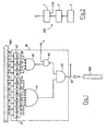
- Fig. 1 schematically shows a programmable memory register (redundancy register) provided in a memory device to implement redundancy.
- the redundancy register RR comprises a plurality of programmable memory units MU0-MU10, each one capable of storing a binary information unit.
- Each one of the memory units MU0-MU10 is supplied by a respective address signal A0-A10 taken from an address signal bus ADD of the memory device.
- memory devices comprise a matrix of memory cells arranged in row (word lines) and columns (bit lines); A0-A10 can be for example the row address signals which are decoded for selecting one of the word lines of the memory matrix; in alternative, A0-A10 can be the column address signals which are decoded for selecting one of the bit lines of the memory matrix. As shown schematically in Fig.
- Each memory unit MUi generates a respective output signal Oi which is activated (at the high logic level) when the respective current address signal Ai coincides with the datum stored in the respective memory element.
- the memory units MU0-MU10 are grouped in two groups: a first group G1 comprises for example the seven memory units MU4-MU10, associated to the seven most-significant address bits A4-A10; a second group G2 comprises the remaining four memory units MU0-MU3 associated with the four least-significant address bits A0-A3. Other divisions of the plurality of memory units MU0-MU10 among the two groups G1 and G2 are also possible.
- the output signals O0-O3 of the second group G2 of memory units MU0-MU3 supply a first NAND gate N1; the output signals O4-O10 of the first group G1 of memory units MU4-MU10 supply an AND gate A1.
- An output signal of NAND gate N1 supplies a first input of a second NAND gate N2; a second input of NAND gate N2 is supplied by a forcing signal F, which is normally kept at the low logic level and is activated in a particular test mode, as will be explained in greater detail in the following.
- An output signal of AND gate A1 and an output signal of NAND gate N2 supply a third NAND gate N3.
- An output signal RS of NAND gate N3 is activated (at the low Logic level) only when the current address signals A0-A10 coincides with the address stored in the memory units MU0-MU10.
- Signal RS allows the selection of a respective redundancy memory element RME (for example a redundancy word line or a redundancy bit line).
- RME redundancy memory element
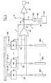
- redundancy memory elements RME1-RMEn are normally provided in a memory device (again, redundancy memory elements RME1-RMEn can be either redundancy word lines or redundancy bit lines).
- redundancy memory elements RME1-RMEn can be either redundancy word lines or redundancy bit lines.
- a respective redundancy register RR1-RRn having the structure shown in Fig. 1 must be provided; each one of the redundancy registers RR1-RRn generates a respective redundancy element selection signal RS1-RSn which is activated when the current address signals A0-A10 coincide with the address stored in the respective memory units MU0-MU10.
- the redundancy selection signals RS1-RSn are supplied to a first OR gate OR1.
- An output signal RD of OR gate OR1 is coupled to an output buffer OB through a switch SW controlled by a test signal T1.
- Switch SW allows to switch the input of output buffer OB between signal RD and a data signal D carrying a datum obtained through the conventional read path of the memory device.
- Signal T1 is generated by a second OR gate OR2 which receives at its inputs two test signals NED and FN, generated by a control logic CNT which is normally provided in the memory device; signal FN is the logic complement of signal F, the latter being generated by an inverter I1.
- Output buffer OB drives an output terminal OT (output pad) of the memory device.
- the current address supplied to the memory device is compared, by the redundancy registers RR1-RRn, with the defective addresses stored therein.
- the signals RS1-RSn are not activated, and no redundancy memory element is selected.
- test signals FN and NED are both deactivated, so that switch SW connects the input of output buffer OB to the data signal D, which carries the result of the sensing operation of an addressed memory cell of the memory matrix.
- the redundancy register RR1-RRn wherein such defective address is stored activates the respective redundancy selection signal RS1-RSn (referring to Fig. 1, all the signals O0-O10 are activated).
- the activation of one redundancy selection signal RS1-RSn inhibits the selection of the defective word line or bit line, and enables the selection of the associated redundancy memory element RME1-RMEn.
- test signals FN and NED are deactivated, and switch SW connects the input of output buffer OB with the data signal D.
- control logic CNT activates signal NED: in this way, switch SW connectes the input of output buffer OB to the output RD of OR gate OR1.
- address signals A0-A10 which in this example are 2 11
- each time the memory device is supplied with an address configuration corresponding to one of the defective addresses stored in the redundancy registers RR1-RRn one of the redundancy selection signals RS1-RS2 will be activated, and the signal RD will also be activated.
- a logic-level transition will be detected at the output terminal OT of the memory device: it is thus possible to determine which address configurations correspond to defective addresses.
- This new test mode is activated by activating the signal FN which, as visible in Fig. 1, forces the output of NAND N2 to a Logic "1" independently of the output of NAND N1, i.e. independently of the value of signals O0-O3.
- n is the number of redundancy memory elements RME1-RMEn.
- RME1-RMEn the number of different address configurations which must be scanned.
- n the number of redundancy memory elements
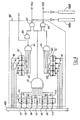
- Fig. 4 schematically shows another embodiment of a redundancy register RR'.
- the redundancy register RR' comprises a first group G1' of programmable memory units MU4-MU10, associated to the address signals A4-A10, a second group G2' of programmable memory units MU01-MU31 associated to the address signals A0-A3, and a third group G2" of programmable memory units MU02-MU32 also associated to the address signals A0-A3.
- the first group G1' of memory units stores the common part of two defective addresses; the second group G2' of memory units MU01-MU31 stores the remaining part of one of the two defective addresses; the third group G2" of memory units MU02-MU32 stores the remaining part of the other of the two defective addresses.
- This structure of the redundancy register is particularly suitable in some kinds of memory devices, wherein there is a high probability that when a defective matrix word line or bit line exists, also the adjacent word line or bit line is defective: since adjacent word lines or bit lines generally have part of their addresses in common, it is advantageous to use a dual redundancy register instead of using two redundancy registers of the type shown in Fig. 1.
- Output signals O4-O10 of the first group G1' of memory units supply a first AND gate A2.
- Output signals O01-O31 of the second group G2' of memory units supply a first NAND gate N4.
- Output signals O02-O32 of the third group G2" of memory units supply a second AND gate A3.
- An output signal of AND gate A2 and an output signal of AND gate A3 supply a second NAND gate N5.
- An output signal of NAND gate N4 supplies a first input of a third NAND gate N6 whose second input is supplied by the forcing signal F.
- An output signal of NAND gate N6 supplies a first input of a fourth NAND gate N7 whose second input is supplied by the output signal of AND gate A2.
- An output signal RSA of NAND gate N7 allows the selection of a first redundancy memory element RMEA associated to the redundancy register RR'; an output signal RSB of NAND gate N5 allows the selection of a second redundancy memory element RMEB associated to the redundancy register RR'.
- Fig. 5 is similar to Fig. 3: a plurality of dual redundancy registers RR1'-RRn' is shown, each one associated to two respective redundancy memory elements RMEA1-RMEAn and RMEB1-RMEBn.
- the redundancy selections signals RSA1-RSAn and RSB1-RSBn generated by the dual redundancy registers RR1'-RRn' supply an OR gate OR3; an output of OR gate OR3 can be selectively connected to an output buffer OB by means of a switch SW, controlled by a test signal T1; signal T1 is again the logic OR of signals FN and NED, generated by the control logic CNT.
- a first technique is conventional and provides for sequentially scanning all the possible configurations of address signals A0-A10; this test mode is entered by activating the signal NED.
- a second technique is new and faster than the conventional one: it provides for forcing the output of NAND gate N6 in each redundancy register to a predetermined logic level equal to the Logic level it would assume if the configuration of address signals A0-A3 were equal to the address configuration stored in the memory units MU01-MU31 of the second group G2'; then, only the address signals A4-A10 are scanned, so that when the configuration of signals A4-A10 coincides with the one stored in the first group G1' of memory units MU4-MU10 of one of the redundancy registers RR1'-RRn', the respective redundancy selection signal RSA1-RSAn is activated, and a logic level transition takes place at the output terminal OT: when such a transition is detected, the current configuration
- the present invention is not limited to the particular embodiments previously described; in particular, the number of memory units of the groups G1 and G2 or G1', G2' and G2" could be varied (obviously, the higher the number of memory units of group G1 or G1', the lower the number of memory units of group G2 or groups G2' and G2").
Landscapes
- For Increasing The Reliability Of Semiconductor Memories (AREA)
Description
Claims (13)
- Method for detecting redunded defective addresses in a memory device with redundancy comprising at least one memory register (RR1-RRn;RR1'-RRn') for storing at least one defective address, said memory register comprising a plurality of memory units (MU0-MU10) each one storing a defective address bit and comparing said defective address bit with a respective current address bit (A0-A10) of a current address supplied to the memory device, the memory register activating a respective redundancy selection signal (RS1-RSn;RSA1-RSAn,RSB1-RSBn) when the current address coincides with the at least one defective address stored therein, characterized by providing for:a) activating a forcing signal (F) for forcing the activation of said redundancy selection signal to be independent of the coincindence of a first group (A0-A3) of current address bits, associated to a respective first group (G2) of said memory units, with the defective address bits stored in said respective first group (G2) of memory units;b) scanning all the possible configurations of a second group (A4-A10) of current address bits associated to a second group (G1) of said memory units and sequentially supplying the memory device with all said configurations;c) detecting a configuration of said second group (A4-A10) of current address bits for which said redundancy selection signal is activated;d) while supplying the memory device with said configuration of the second group (A4-A10) of current address bits, deactivating said forcing signal and sequentially supplying the memory device with a scanning of all the possible configurations of said first group (A0-A3) of address bits;e) detecting a configuration of said first group (A0-A3) of current address bits for which said redundancy selection signal is activated.
- Method according to claim 1, the memory register (RR1'-RRn') being suitable to store two defective addresses with a common defective address part and comprising a second group (G1') of memory units for storing said common defective address part and two first groups (G2',G2") of memory units each one storing a remaining part of a respective one of the two defective addresses, the memory register activating either a first (RSA1-RSAn) or a second (RSB1-RSBn) redundancy selection signals when the current address supplied to the memory device coincides with either one or the other of said two defective addresses, characterized by providing for:a) activating the forcing signal (F) for forcing the activation of the first redundancy selection signal (RSA1-RSAn) to be independent of the coincindence of the first group (A0-A3) of current address bits, associated to said two first groups (G2',G2") of memory units, with the defective address bits stored in one (G2') of said two first groups of memory units;b) scanning all the possible configurations of a second group (A4-A10) of current address bits associated to the second group (G1') of memory units and sequentially supplying the memory device with all said configurations;c) detecting a configuration of said second group (A4-A10) of current address bits for which said first redundancy selection signal (RSA1-RSAn) is activated;d) while supplying the memory device with said configuration of the second group (A4-A10) of current address bits, deactivating said forcing signal and sequentially supplying the memory device with a scanning of all the possible configurations of said first group (A0-A3) of address bits;e) detecting the two configurations of said first group (A0-A3) of current address bits for which the first (RSA1-RSAn) and the second (RSB1-RSBn) redundancy selection signals are respectively activated.
- Method according to claim 1 or 2, the memory device comprising a plurality of memory registers (RR1-RRn;RR1'-RRn') each one storing at least one defective address and activating a respective redundancy selection signal (RS1-RSn;RSa1-RSAn,RSB1-RSBn) when the current address supplied to the memory device coincides with the at least one defective address stored therein, characterized in that steps d) and e) are repeated for all the configurations of said second group (A4-A10) of current address bits for which during step c) the activation of one of the redundancy selection signals is detected.
- Method according to anyone of the preceding claims, characterized in that said first group (A0-A3) and second group (A4-A10) of current address bits form a column address for selecting a column of memory cells of the memory device.
- Method according to anyone of claims 1 to 3, characterized in that said first group (A0-A3) and second group (A4-A10) of current address bits form a row address for selecting a row of memory cells of the memory device.
- Redundancy circuit for a memory device, comprising at least one redundancy memory register (RR1-RRn;RR1'-RRn') for storing at least one defective address, said redundancy memory register comprising a plurality of memory units (MU0-MU10) each one storing a defective address bit and comparing said defective address bit with a respective current address bit (A0-A10) of a current address supplied to the redundancy memory register, the redundancy memory register activating a respective redundancy selection signal (RS1-RSn;RSA1-RSAn,RSB1-RSBn) when the current address coincides with the at least one defective address stored therein, characterized in that the redundancy memory register comprises forcing means (N1-N3;N4,N6,N7) controlled by a forcing signal (F) activated in a test condition for forcing the activation of the redundancy selection signal to be independent of the coincindence of a first group (A0-A3) of current address bits, associated to a respective first group (G2) of said memory units, with the defective address bits stored in said respective first group (G2) of memory units, the redundancy circuit comprising means for carrying out the detection of the defective address stored in the redundancy register by sequentially supplying the redundancy memory register with all the possible configurations of a second group (A4-A10) of current address bits associated to a second group (G1) of memory units to detect a configuration of said second group (A4-A10) of current address bits for which the redundancy selection signal is activated, and while maintaining said configuration of the second group (A4-A10) of current address bits, deactivating the forcing signal and scanning all the configurations of the first group (A0-A3) of address bits.
- Redundancy circuit according to claim 6, characterized in that each memory unit (MU0-MU10) comprises a programmable memory element (1), a sensing circuit (2) for reading a datum stored in the memory element and comparator means (3) for comparing the datum stored in the memory element with the respective current address bit (A0-A10), said comparator means activating a comparison signal (O0-O10) when the datum stored in the memory element coincides with the respective current address bit.
- Redundancy circuit according to claim 7, characterized in that the redundancy register comprises first logic gate (A1) for activating a first output signal when the comparison signals (O4-O10) of said second group (G1) of memory units are all activated, said forcing means (N1-N3) comprising a second logic gate (N1) for activating a second output signal when the comparison signals (O0-O3) of said first group (G2) of memory units are all activated, a third logic gate (N2) supplied by said second output signal and said forcing signal (F) for activating a third output signal when either the second logic signal is activated or the forcing signal is activated, and a fourth logic gate (N3) supplied by said first output signal and third output signal for activating said redundancy selection signal (RS1-RSn) when both the first output signal and the third output signal are activated.
- Redundancy circuit according to claim 6, the memory register (RR1'-RRn') being suitable to store two defective addresses with a common defective address part and comprising a second group (G1') of memory units for storing said common defective address part and two first groups (G2',G2'') of memory units each one storing a remaining part of a respective one of the two defective addresses, the memory register activating either a first (RSA1-RSAn) or a second (RSB1-RSBn) redundancy selection signals when the current address supplied to the memory device coincides with either one or the other of said two defective addresses, characterized in that said forcing means (N4,N6,N7) force the activation of the first redundancy selection signal (RSA1-RSAn) to be independent of the coincidence of the first group (A0-A3) of the current address bits, associated with said two first groups (G2',G2'') of memory units, with the defective address bits stored in one (G2') of said two first groups of memory units.
- Redundancy circuit according to anyone of claims 6 to 9, characterized by comprising a plurality of memory registers (RR1-RRn;RR1'-RRn') each one storing at least one defective address and activating a respective redundancy selection signal (RS1-RSn;RSA1-RSAn,RSB1-RSBn) when the current address supplied to the memory device coincides with the at least one defective address stored therein.
- Redundancy circuit according to anyone of claims 6 to 10, characterized in that said first group (A0-A3) and second group (A4-A10) of current address bits form a column address for selecting a column of memory cells of the memory device.
- Redundancy circuit according to anyone of claims 6 to 10, characterized in that said first group (A0-A3) and second group (A4-A10) of current address bits form a row address for selecting a row of memory cells of the memory device.
- Redundancy circuit according to anyone of claims 6 to 12, characterized in that said forcing signal is generated by a control logic internal to the memory device.
Priority Applications (4)
| Application Number | Priority Date | Filing Date | Title |
|---|---|---|---|
| DE69626625T DE69626625T2 (en) | 1996-04-18 | 1996-04-18 | Method for detecting redundant faulty addresses in a memory arrangement with redundancy |
| EP96830216A EP0802541B1 (en) | 1996-04-18 | 1996-04-18 | Method for detecting redundant defective addresses in a memory device with redundancy |
| US08/841,904 US5838623A (en) | 1996-04-18 | 1997-04-17 | Method for detecting redunded defective addresses in a memory device with redundancy |
| US09/183,469 US5936907A (en) | 1996-04-18 | 1998-10-30 | Method for detecting redunded defective addresses in a memory device with redundancy |
Applications Claiming Priority (1)
| Application Number | Priority Date | Filing Date | Title |
|---|---|---|---|
| EP96830216A EP0802541B1 (en) | 1996-04-18 | 1996-04-18 | Method for detecting redundant defective addresses in a memory device with redundancy |
Publications (2)
| Publication Number | Publication Date |
|---|---|
| EP0802541A1 EP0802541A1 (en) | 1997-10-22 |
| EP0802541B1 true EP0802541B1 (en) | 2003-03-12 |
Family
ID=8225882
Family Applications (1)
| Application Number | Title | Priority Date | Filing Date |
|---|---|---|---|
| EP96830216A Expired - Lifetime EP0802541B1 (en) | 1996-04-18 | 1996-04-18 | Method for detecting redundant defective addresses in a memory device with redundancy |
Country Status (3)
| Country | Link |
|---|---|
| US (2) | US5838623A (en) |
| EP (1) | EP0802541B1 (en) |
| DE (1) | DE69626625T2 (en) |
Families Citing this family (6)
| Publication number | Priority date | Publication date | Assignee | Title |
|---|---|---|---|---|
| EP0802541B1 (en) * | 1996-04-18 | 2003-03-12 | STMicroelectronics S.r.l. | Method for detecting redundant defective addresses in a memory device with redundancy |
| US7930592B2 (en) * | 2002-12-16 | 2011-04-19 | International Business Machines Corporation | Enabling memory redundancy during testing |
| ATE448547T1 (en) * | 2002-12-16 | 2009-11-15 | Ibm | ACTIVATION OF STORAGE REDUNDANCY DURING TESTING |
| US7304901B2 (en) * | 2002-12-16 | 2007-12-04 | International Business Machines Corporation | Enabling memory redundancy during testing |
| KR100763357B1 (en) | 2005-05-13 | 2007-10-04 | 인터내셔널 비지네스 머신즈 코포레이션 | Enable memory redundancy during testing |
| KR20190060527A (en) | 2017-11-24 | 2019-06-03 | 삼성전자주식회사 | Semiconductor memory device and method of operating the same |
Family Cites Families (4)
| Publication number | Priority date | Publication date | Assignee | Title |
|---|---|---|---|---|
| KR950008676B1 (en) * | 1986-04-23 | 1995-08-04 | 가부시기가이샤 히다찌세이사꾸쇼 | Semiconductor memory device and defect repair method thereof |
| US5381370A (en) * | 1993-08-24 | 1995-01-10 | Cypress Semiconductor Corporation | Memory with minimized redundancy access delay |
| FR2716743B1 (en) * | 1994-02-28 | 1996-09-27 | Sgs Thomson Microelectronics | Memory redundancy circuit. |
| EP0802541B1 (en) * | 1996-04-18 | 2003-03-12 | STMicroelectronics S.r.l. | Method for detecting redundant defective addresses in a memory device with redundancy |
-
1996
- 1996-04-18 EP EP96830216A patent/EP0802541B1/en not_active Expired - Lifetime
- 1996-04-18 DE DE69626625T patent/DE69626625T2/en not_active Expired - Fee Related
-
1997
- 1997-04-17 US US08/841,904 patent/US5838623A/en not_active Expired - Lifetime
-
1998
- 1998-10-30 US US09/183,469 patent/US5936907A/en not_active Expired - Lifetime
Also Published As
| Publication number | Publication date |
|---|---|
| US5936907A (en) | 1999-08-10 |
| DE69626625T2 (en) | 2003-10-02 |
| US5838623A (en) | 1998-11-17 |
| DE69626625D1 (en) | 2003-04-17 |
| EP0802541A1 (en) | 1997-10-22 |
Similar Documents
| Publication | Publication Date | Title |
|---|---|---|
| US7159141B2 (en) | Repairable block redundancy scheme | |
| US5153880A (en) | Field-programmable redundancy apparatus for memory arrays | |
| US5493531A (en) | Integrated circuitry for checking the utilization rate of redundancy memory elements in a semiconductor memory device | |
| US5161157A (en) | Field-programmable redundancy apparatus for memory arrays | |
| EP0806773B1 (en) | Electrically erasable and programmable non-volatile memory device with testable redundancy circuits | |
| EP1447813B1 (en) | Memory built-in self repair (MBISR) circuits / devices and method for repairing a memory comprising a memory built-in self repair (MBISR) structure | |
| JP2588692B2 (en) | Redundant register programming method and column redundant integrated circuit | |
| JP2791288B2 (en) | Method of programming a redundant register in a row redundant integrated circuit for a semiconductor memory device and a row redundant integrated circuit | |
| JPH07201196A (en) | Dynamic redundancy circuit for integrated circuit memory | |
| JP2540028B2 (en) | Integrated programming circuit | |
| EP0802541B1 (en) | Method for detecting redundant defective addresses in a memory device with redundancy | |
| US5708601A (en) | Integrated circuitry for checking the utilization rate of redundancy memory elements in a semiconductor memory device | |
| US6108250A (en) | Fast redundancy scheme for high density, high speed memories | |
| US5867504A (en) | Semiconductor memory device with row and column redundancy circuits and a time-shared redundancy circuit test architecture. | |
| US5831915A (en) | Memory device with clocked column redundancy | |
| US6198675B1 (en) | RAM configurable redundancy | |
| EP0811917B1 (en) | Circuit for transferring redundancy data of a redundancy circuit inside a memory device by means of a time-shared approach | |
| EP0811918B1 (en) | Semiconductor memory device with clocked column redundancy and time-shared redundancy data transfer approach | |
| EP0811988B1 (en) | Semiconductor memory device with row and column redundancy circuits and a time-shared redundancy circuit test architecture | |
| US20010026498A1 (en) | Memory configuration having a circuit for determining the activated memory array | |
| EP0797144A1 (en) | Circuit for detecting the coincidence between a binary information unit stored therein and an external datum |
Legal Events
| Date | Code | Title | Description |
|---|---|---|---|
| PUAI | Public reference made under article 153(3) epc to a published international application that has entered the european phase |
Free format text: ORIGINAL CODE: 0009012 |
|
| AK | Designated contracting states |
Kind code of ref document: A1 Designated state(s): DE FR GB IT |
|
| 17P | Request for examination filed |
Effective date: 19980411 |
|
| RAP3 | Party data changed (applicant data changed or rights of an application transferred) |
Owner name: STMICROELECTRONICS S.R.L. |
|
| GRAG | Despatch of communication of intention to grant |
Free format text: ORIGINAL CODE: EPIDOS AGRA |
|
| 17Q | First examination report despatched |
Effective date: 20020517 |
|
| GRAG | Despatch of communication of intention to grant |
Free format text: ORIGINAL CODE: EPIDOS AGRA |
|
| GRAH | Despatch of communication of intention to grant a patent |
Free format text: ORIGINAL CODE: EPIDOS IGRA |
|
| GRAH | Despatch of communication of intention to grant a patent |
Free format text: ORIGINAL CODE: EPIDOS IGRA |
|
| GRAA | (expected) grant |
Free format text: ORIGINAL CODE: 0009210 |
|
| AK | Designated contracting states |
Designated state(s): DE FR GB IT |
|
| REG | Reference to a national code |
Ref country code: GB Ref legal event code: FG4D |
|
| REF | Corresponds to: |
Ref document number: 69626625 Country of ref document: DE Date of ref document: 20030417 Kind code of ref document: P |
|
| ET | Fr: translation filed | ||
| PLBE | No opposition filed within time limit |
Free format text: ORIGINAL CODE: 0009261 |
|
| STAA | Information on the status of an ep patent application or granted ep patent |
Free format text: STATUS: NO OPPOSITION FILED WITHIN TIME LIMIT |
|
| 26N | No opposition filed |
Effective date: 20031215 |
|
| PGFP | Annual fee paid to national office [announced via postgrant information from national office to epo] |
Ref country code: DE Payment date: 20040329 Year of fee payment: 9 |
|
| PG25 | Lapsed in a contracting state [announced via postgrant information from national office to epo] |
Ref country code: IT Free format text: LAPSE BECAUSE OF NON-PAYMENT OF DUE FEES;WARNING: LAPSES OF ITALIAN PATENTS WITH EFFECTIVE DATE BEFORE 2007 MAY HAVE OCCURRED AT ANY TIME BEFORE 2007. THE CORRECT EFFECTIVE DATE MAY BE DIFFERENT FROM THE ONE RECORDED. Effective date: 20050418 |
|
| PG25 | Lapsed in a contracting state [announced via postgrant information from national office to epo] |
Ref country code: DE Free format text: LAPSE BECAUSE OF NON-PAYMENT OF DUE FEES Effective date: 20051101 |
|
| PGFP | Annual fee paid to national office [announced via postgrant information from national office to epo] |
Ref country code: GB Payment date: 20080326 Year of fee payment: 13 |
|
| GBPC | Gb: european patent ceased through non-payment of renewal fee |
Effective date: 20090418 |
|
| REG | Reference to a national code |
Ref country code: FR Ref legal event code: ST Effective date: 20091231 |
|
| PG25 | Lapsed in a contracting state [announced via postgrant information from national office to epo] |
Ref country code: GB Free format text: LAPSE BECAUSE OF NON-PAYMENT OF DUE FEES Effective date: 20090418 Ref country code: FR Free format text: LAPSE BECAUSE OF NON-PAYMENT OF DUE FEES Effective date: 20091222 |
|
| PGFP | Annual fee paid to national office [announced via postgrant information from national office to epo] |
Ref country code: FR Payment date: 20080429 Year of fee payment: 13 |