EP0798618B1 - Array-Anordnung mit Schaltkreisen und Konstantstromquellen für eine Vielzahl von Kanälen - Google Patents
Array-Anordnung mit Schaltkreisen und Konstantstromquellen für eine Vielzahl von Kanälen Download PDFInfo
- Publication number
- EP0798618B1 EP0798618B1 EP97302193A EP97302193A EP0798618B1 EP 0798618 B1 EP0798618 B1 EP 0798618B1 EP 97302193 A EP97302193 A EP 97302193A EP 97302193 A EP97302193 A EP 97302193A EP 0798618 B1 EP0798618 B1 EP 0798618B1
- Authority
- EP
- European Patent Office
- Prior art keywords
- circuits
- array device
- current generating
- constant current
- circuit
- Prior art date
- Legal status (The legal status is an assumption and is not a legal conclusion. Google has not performed a legal analysis and makes no representation as to the accuracy of the status listed.)
- Expired - Lifetime
Links
- 239000004065 semiconductor Substances 0.000 claims description 14
- 230000003287 optical effect Effects 0.000 description 31
- 230000008859 change Effects 0.000 description 27
- 238000010586 diagram Methods 0.000 description 14
- 230000000694 effects Effects 0.000 description 12
- 238000002955 isolation Methods 0.000 description 12
- 230000005540 biological transmission Effects 0.000 description 11
- 238000006243 chemical reaction Methods 0.000 description 7
- 230000033228 biological regulation Effects 0.000 description 6
- 238000005516 engineering process Methods 0.000 description 6
- 230000008054 signal transmission Effects 0.000 description 6
- 230000001629 suppression Effects 0.000 description 6
- 238000000034 method Methods 0.000 description 5
- 230000010355 oscillation Effects 0.000 description 5
- 101710170230 Antimicrobial peptide 1 Proteins 0.000 description 4
- 230000015572 biosynthetic process Effects 0.000 description 4
- 238000004891 communication Methods 0.000 description 4
- 230000004044 response Effects 0.000 description 4
- 239000012080 ambient air Substances 0.000 description 3
- 239000000470 constituent Substances 0.000 description 3
- 230000002238 attenuated effect Effects 0.000 description 2
- 239000003990 capacitor Substances 0.000 description 2
- 230000008878 coupling Effects 0.000 description 2
- 238000010168 coupling process Methods 0.000 description 2
- 238000005859 coupling reaction Methods 0.000 description 2
- 230000002708 enhancing effect Effects 0.000 description 2
- 238000003780 insertion Methods 0.000 description 2
- 230000037431 insertion Effects 0.000 description 2
- 239000000463 material Substances 0.000 description 2
- 239000013307 optical fiber Substances 0.000 description 2
- 239000011295 pitch Substances 0.000 description 2
- 230000001737 promoting effect Effects 0.000 description 2
- 230000000644 propagated effect Effects 0.000 description 2
- 230000009467 reduction Effects 0.000 description 2
- 229920006395 saturated elastomer Polymers 0.000 description 2
- 229910001218 Gallium arsenide Inorganic materials 0.000 description 1
- 230000003321 amplification Effects 0.000 description 1
- 239000011111 cardboard Substances 0.000 description 1
- 238000012937 correction Methods 0.000 description 1
- 238000013461 design Methods 0.000 description 1
- 238000011161 development Methods 0.000 description 1
- 239000006185 dispersion Substances 0.000 description 1
- 230000001747 exhibiting effect Effects 0.000 description 1
- 238000004519 manufacturing process Methods 0.000 description 1
- 238000003199 nucleic acid amplification method Methods 0.000 description 1
- 230000006641 stabilisation Effects 0.000 description 1
- 238000011105 stabilization Methods 0.000 description 1
Images


Classifications
-
- G—PHYSICS
- G05—CONTROLLING; REGULATING
- G05F—SYSTEMS FOR REGULATING ELECTRIC OR MAGNETIC VARIABLES
- G05F1/00—Automatic systems in which deviations of an electric quantity from one or more predetermined values are detected at the output of the system and fed back to a device within the system to restore the detected quantity to its predetermined value or values, i.e. retroactive systems
- G05F1/10—Regulating voltage or current
- G05F1/46—Regulating voltage or current wherein the variable actually regulated by the final control device is dc
- G05F1/56—Regulating voltage or current wherein the variable actually regulated by the final control device is dc using semiconductor devices in series with the load as final control devices
- G05F1/577—Regulating voltage or current wherein the variable actually regulated by the final control device is dc using semiconductor devices in series with the load as final control devices for plural loads
-
- H—ELECTRICITY
- H01—ELECTRIC ELEMENTS
- H01L—SEMICONDUCTOR DEVICES NOT COVERED BY CLASS H10
- H01L2924/00—Indexing scheme for arrangements or methods for connecting or disconnecting semiconductor or solid-state bodies as covered by H01L24/00
- H01L2924/0001—Technical content checked by a classifier
- H01L2924/0002—Not covered by any one of groups H01L24/00, H01L24/00 and H01L2224/00
Definitions
- the present invention relates in general to an array device having functional circuits for a plurality of channels such as optical receiver modules for optical interconnection or like optical receiver modules, and more particularly to an array device including current generating circuits which are capable of supplying the same current to the functional circuits for a plurality of channels.
- the success in the optical communication technology shows that for the signal transmission of the high speed, large capacity and long distance, the procedure that an electrical signal is temporarily converted into light and the resultant light signal is transmitted through a transmission line formed of optical fibers is more advantageous than the procedure that an electrical signal is directly transmitted as it is. That is, it is shown that the light transmission in which the electro-optic and opto-electric conversion function is introduced into a system is excellent in terms of practical use.
- FIG. 1 is a circuit diagram showing a transmission driver as a main portion of the optical transmitter module.
- the transmission driver has transistors Q1 and Q2, and to bases thereof are inputted inputs 1 and 2, respectively.
- a constant current circuit 100X is connected to each of emitters of the transistors Q1 and Q2.
- a load DIODE is connected to a collector of the transistor Q2. The load DIODE is also connected to a constant current circuit 100X' in order to secure a high speed operation in the transmission driver.
- FIG. 2 is a circuit diagram showing a configuration of a receiver circuit as a main portion of an optical receiver module.
- the incident light signal is converted into a current signal I IN through a photodiode and an output is obtained from a transimpedance amplifier ZAMP.
- a constant current generating circuit 100Y is used to compensate for a dark current of the photodiode and also to apply an offset to the input current signal.
- the array device constituting the optical interconnect module is configured, from the circumstances in which the characteristics of the individual original constituent elements are equal to each other, in such a way as to have only to be able to supply the same current to all the constant current generating circuits of the channels.
- the high speed parallel type integrated circuit since the high speed parallel type integrated circuit has the configuration in which the power sources and the grounding points are provided independently for every circuit in many cases, the constant current generating circuits thereof are necessarily provided independently of one another.
- the power sources and the ground lines are respectively made common so that the current to be caused to flow is controlled from one common terminal.
- FIG. 3 there is shown an equivalent circuit diagram, as a prior art example, of a circuit which is designed in such a way that circuits of multiple channels are controlled at the same time by one common voltage.
- FIG. 4 there is shown the outline of an arrangement of current generating circuit blocks 100A' (301', 201', and 101') to 100N' (30n', 20n' and 10n') of channels and functional circuit blocks 401' and 402' to 40n' which are formed on an integrated circuit chip 1'.
- a control signal VCTRL which has been inputted to a control signal input terminal IN is caused to flow through the positions of the current generating control blocks 100A' (301', 201' and 101') to 100N' (30n', 20n' and 10n') of the channels which are arranged in the distributed positions on the integrated circuit chip so as to generate the desired currents therefrom, and also the circuit blocks 401' and 402' to 40n' to which the constant currents are supplied from the respective current generating circuit blocks 100A' to 100N' are also distributively arranged on the integrated circuit chip.
- reference numerals 301' and 302' to 30n' designate respectively input circuits each comprised of an active circuit or a low-pass filter.
- the semiconductor laser is employed in order to convert an electrical signal into a light signal.
- the semiconductor laser device has the property in which the characteristics thereof are sensitive to the change in the temperature, and the influence of the temperature change appears in the form of increase of the lasing threshold and reduction in the efficiency of converting the current into light. Then, both the change in the optical output and the change in the frequency bandwidth resulting from the temperature change in the oscillation threshold and the conversion efficiency influence directly the signal transmission characteristics of the optical interconnect module.
- a control circuit is incorporated therein to be used which is designed in such a way as to monitor the intensity of a laser output beam so as for the laser output beam to maintain the fixed average intensity at all times.
- a control circuit is incorporated therein to be used which is designed in such a way as to monitor the intensity of a laser output beam so as for the laser output beam to maintain the fixed average intensity at all times.
- the circuit system has been adopted such that with respect to the signal which is used to control the output current of FIG. 3, the input voltage is made constant and also the output current is kept constant as much as possible.
- the signal transmission characteristics of the optical interconnect module are changed in such a way that: the dynamic range of an input of the receiver circuit becomes narrow; the error rate is changed along with the change in the ambient air temperature; and the band width is changed.
- the transmission functional circuit blocks for a plurality of channels constituting the parallel optical interconnect module requires the constant current source in which the current to be supplied can be controlled from the outside, and also it is essential thereto that all the channels can be controlled at the same time by one common voltage signal.
- the semiconductor laser devices each of which serves to convert the electrical signal into the optical signal are respectively employed in the transmission functional blocks, the semiconductor laser device has the feature that its output is changed along with the temperature change and the current change.
- the transmission functional circuit blocks are provided so as to correspond to a plurality of channels, and hence in order to make the output adjustable, the constant current source is required in which the current value of the driving signal which is supplied to each of the transmission functional circuit blocks can be controlled from the outside.
- the constant current source is required in which the current value of the driving signal which is supplied to each of the transmission functional circuit blocks can be controlled from the outside.
- an array device having functional circuits for a plurality of channels. That is, an array device including functional circuits for a plurality of channels, constant current generating circuits for the plurality of channels for generating constant currents used to drive the functional circuits, respectively, in accordance with a control signal supplied from the outside, and a wiring for supplying therethrough the constant currents from the constant current generating circuits to the functional circuits, respectively, which are formed on an integrated circuit chip may provide that the constant current generating circuits provided so as to correspond to the channels are arranged concentratedly in a specific region on the integrated circuit chip, and the wiring is comprised of a common wiring extending from one terminal provided in the vicinity of the specific region to the vicinities of the constant current generating circuits.
- each of the constant current generating circuits is configured in such a way as not to need to take the correction for the offset and the like into consideration in advance at all so that the current characteristics can be made equal to one another on the. basis of the common control signal without the external adjustment.
- an array device including functional circuits for a plurality of channels, constant current generating circuits for the plurality of channels for generating constant currents used to drive the functional circuits, respectively, in accordance with a control signal supplied from the outside, and a wiring for supplying therethrough the constant currents from the constant current generating circuits to the functional circuits, respectively, which are formed on an integrated circuit chip may provide that the constant current generating circuits provided so as to correspond to the channels are arranged on the integrated circuit chip in accordance with a regular relationship, and each of the constant current generating circuits includes a grounded-emitter transistor, an input resistor connected to a base of the transistor, and an emitter resistor connected to an emitter of the transistor, and that the wiring is comprised of a common wiring extending from one terminal to the vicinities of the constant current generating circuits.
- the resistance value of the grounding wiring between the channels can be quantitatively grasped.
- the circuit configuration in which the offset is corrected in advance can be made possible, and also the characteristics of the currents which are generated from the constant current generating circuits, respectively, can be made equal to one another on the basis of the common control signal without the external adjustment.
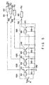
- FIG. 5 shows a circuit of an array device of an embodiment of the present invention
- FIG. 6 shows a layout of that circuit shown in FIG. 5 on a chip.
- an input terminal for a control signal V CTRL is provided on a chip.
- Current generating circuit blocks 100A to 100N for a plurality of channels are also provided on the same chip.
- functional circuit blocks 401 to 40n for a plurality of channels are also provided on the same chip.
- the current generating circuit blocks 100A to 100N for the channels receive the control signal voltage VCTRL which has been inputted through the input terminal IN and generate, in response to the control signal voltage VCTRL, current outputs each having the desired current value, and supply the currents thus generated to the functional circuit blocks 401 to 40n for the channels, respectively.
- the functional circuit blocks 401 to 40n for the channels carry out the predetermined operations in accordance with the currents thus supplied thereto.
- the current generating circuit blocks 100A to 100N are provided with input circuits 301, 302 and 303 to 30n each comprised of an active circuit or a low-pass filter, respectively.
- the current generating circuit blocks 100A to 100N are provided with emitter resistors 201, 202 and 203 to 20n, respectively.
- both the current generating circuit blocks 100A to 100N for the channels and the functional circuit blocks 401 to 40n for the channels are formed on an IC chip 1.
- the IC chip 1 is divided into an area in which the functional circuit blocks 401 to 40n are formed and an area in which the current generating circuit blocks 100A to 100N are formed.
- the functional circuit blocks 401 to 40n for the channels are arranged in this order, and in the formation area for the current generating circuit blocks, the current generating circuit blocks 100A to 100N for the channels are arranged in this order.
- the one input terminal IN is provided in the vicinity of the formation area for the current generating circuit blocks, and the control signal voltage VCTRL which has been inputted through the input terminal IN is supplied to each of the current generating circuit blocks 100A to 100N.
- the current generating circuit blocks 100A to 100N are collectively arranged in the formation area for the current generating circuit blocks, whereby the wiring for distributing therethrough the control signal voltage VCTRL from the common input terminal IN to the current generating circuit blocks 100A to 100N can be made short so that the wiring resistances can be substantially ignored and also the current generating circuit blocks 100A to 100N can be operated under the same circuit condition.
- the current generating circuit blocks 100A to 100N are configured by employing respective transistors, and generate, in response to the inputted control signal voltage VCTRL, the currents and also supply the currents thus generated to the corresponding functional circuit blocks 401 to 40n, respectively.
- control signal voltage VCTRL is distributed through the control signal wirings from the common input terminals IN to a plurality of current generating circuit blocks 100A to 100N
- the current generating circuit blocks are concentratedly arranged in one area
- the electrical conditions for the current generating circuit blocks 100A to 100N are approximately the same.
- the functional circuit blocks 401 to 40n are also concentratedly arranged in the other one area, the electrical conditions for the functional circuit blocks 401 to 40n are approximately the same.
- the current generating circuit blocks 100A to 100N include grounded-emitter npn transistors 101 to 10n, respectively. Then, when the control signal voltage VCTRL is supplied to the bases of the transistors 101 to 10n, the current generating circuit blocks 100A to 100N generate, in response to the control signal voltage VCTRL, the currents and then supply the currents thus generated to the corresponding functional circuit blocks 401 to 40n.
- the current generating circuit blocks 100A to 100N are collectively arranged in the same area, whereby the length of the wiring can be shortened and also when distributing the current signal voltage VCTRL from the input terminal IN to the current generating circuit blocks through the wirings, the differences between the voltage drops due to the wiring resistances and the offset voltages in the ground line, to which the emitter resistors 201 to 20n are connected in the transistors 101 to 10n, corresponding to the reference ground of the integrated circuit can not occur at all.
- the array device of the present embodiment shown in FIG. 5 has the feature that the device is, as shown in FIG. 6, laid out on the IC chip 1. That is, in the case of the configuration of the conventional array device shown in FIG. 3, though one common input terminal for the control signal voltage VCTRL are provided, the constant current generating circuit blocks as the circuits for generating the constant currents, are, as shown in FIG. 4, distributively arranged on the chip 1, and hence the control signal wirings are distributed up to the constant current generating circuit blocks and the control signal voltage VCTRL is supplied to the bases of the transistors in the constant current generating circuits which are arranged away from one another.
- the output impedances are sufficiently high, the wiring impedances up to the functional circuit blocks 401 to 40n which are arranged in the area away from the constant current generating circuit blocks 100A to 100N on the chip 1 do not become a subject of discussion.
- the high frequency signals are provided on the inputs of the functional circuit blocks 401 to 40n to which the collector outputs of the transistors 101 to 10n are connected in the constant current generating circuit blocks 100A to 100N, there is the possibility that the high frequency signals are propagated therethrough so as to leak to the control signal line through the collector to base junction capacitances of the transistors 101 to 10n to cause the crosstalk.
- the crosstalk of the high frequency components increases in quantity because of the capacitive coupling.
- resistors 501 to 50n have only to be respectively inserted between the collectors of the transistors 101 to 10n in the constant current generating circuit blocks 100A to 100N and the inputs of the corresponding functional circuit blocks 401 to 40n in order to increase the respective impedances.
- the crosstalk can be suppressed to a fixed level or less.
- the insertion of the resistors 501 to 50n therebetween offers, in addition to the effect of preventing the leakage of the high frequency signals, the effect of promoting the isolation between the input and the output, and hence contributes to the suppression of the high frequency noises as well as the preventation of the oscillation.
- the resistance values of the inserted resistors 501 to 50n it is desirable to select the large values as long as the collector voltages are dropped due to the voltage drop resulting from the currents flowing through the resistors and also there is no possibility that each of the transistors 101 to 10n are saturated.
- the grounded-base transistor amplifiers AMP1 to AMPn are respectively provided between the constant current generating circuit blocks 100A to 100N and the functional circuit blocks 401 to 40n in order to amplify the respective signals, and also the signals thus amplified are supplied to the corresponding functional circuit blocks 401 to 40n for the channels.
- the output voltages of the collectors of the current generating circuits are stabilized at approximately fixed values, the high frequency isolation between the outputs of the current generating circuits and the inputs of the functional circuit blocks is greatly improved.
- the voltage, of the current generating circuit for controlling each of the values of the constant currents supplied to the functional circuit blocks 401 to 40n, it is effective to use the voltage of a reference voltage generating circuit which is incorporated on the same chip. More specifically, there can be expected the effects: in the case where the reference voltage generating circuit incorporated on the same chip is employed, the commonness of the ground line is kept, and hence the reference voltage is not influenced by the chip current at all; in the case of the reference voltage generating circuit incorporated on the same chip, since any wiring in the outside of the IC is not required, or even if such wiring is required, the scale of the wiring is small, the influence of the noises is reduced; and since the overall chip is kept at the same temperature, for the change in the ambient air temperature, all the circuits are always subjected to the same temperature change and hence the temperature stability of the generated currents is improved, or it is possible to provide consciously the currents thus generated with the specific temperature characteristics.
- a diode is simply used as the means for generating a reference voltage which means is self-contained on the chip since the forward drop voltage thereof is utilized as the reference voltage.
- the forward voltage drop of the diode since the diode as the constituent element is made of the same material as that of the elements constituting the integrated circuit, if the diode is operated under the same condition as that in the elements of the integrated circuit, the same characteristics can be obtained for the diode at all times.
- the change in the base to emitter voltage of the transistor can be compensated by the voltage developed across one diode.
- the simple circuitry since the simple circuitry can be obtained, it is readily made possible that the constant current having the relatively high stability is generated and the current source having the relatively large negative temperature coefficient is configured.
- the band gap reference voltage source is a circuit wherein the temperature coefficient is almost zero and also even if the temperature is changed, the output voltage can be maintained constant. Those characteristics of the band gap reference voltage source are well known.
- FIGS. 8A and 8B show respectively typical examples of the circuit employing the band gap reference voltage source.
- the band gap reference voltage source shown in FIG. 8A includes transistors 11, 12, 13 and 14, resistors 21, 22, 23 and 24, and capacitors 31 and 32.
- the band gap reference voltage source shown in FIG. 8B includes transistors 11, 12, 13, 14, 15 and 16, resistors 22, 23, 24, 25 and 26, and capacitors 31 and 32.
- npn transistors are employed as the active devices constituting the band gap reference voltage source circuit, and also the resistor 21 is provided as the current source.
- the resistor 21 of FIG. 8A is replaced with the constant current source circuit including the pnp transistors 15 and 16, and the resistors 25 and 26.
- both the circuit configurations are functionally equal to each other, and hence even when any one of the configurations is employed, by adjusting the circuit constants, the output voltage Vref can be kept constant against the changes in the temperature and the input voltage of the power supply.
- the resistance values are obtained by making alternations in the optimum value of the constant voltage output, whereby the reference voltage Vref can be made have the positive temperature coefficient or conversely, can be made have the negative temperature coefficient.
- the results when applying concretely the circuit modifying and optimizing the band gap reference power source to the laser driving circuit will hereinbelow be described. That is, for the current generating circuit required for the circuit for driving the laser device, there is preferably adopted the method wherein in order to suppress both the change in the optical output and the change in the frequency bandwidth resulting from the temperature change in the lasing threshold and the conversion efficiency of the laser device so as to keep the signal transmission characteristics constant, the driving current is changed in accordance with the operation temperature change so as to compensate therefor.
- FIG. 9 shows the results when applying concretely the circuit employing the band gap reference power source to the laser driving circuit. As apparent from FIG. 9, it is possible that the negative output voltage change and the positive output voltage change are obtained against the temperature change.
- the current generating circuit which is required for the laser driver circuit there is preferably adopted the method wherein in order to maintain the signal transmission characteristics constant, the driving current is changed in accordance with the temperature change so as to compensate therefor.
- the recent laser for the optical interconnection has the lower threshold, and in addition thereto, the temperature characteristics of the threshold and the conversion efficiency have been considerably improved and also the recent laser has the characteristics in which the temperature dependency thereof is changed on the basis of a certain regulation. That is, for the circuit for generating the oscillation threshold and the pulse driving current, instead of the circuit for generating a constant current in such a way as in the prior art, the circuit for changing the output current in accordance with a certain regulation in such a way as to compensate for the temperature characteristics of the semiconductor laser, i.e., the feedforward type circuit is effective.
- FIG. 9 is a characteristic view showing the temperature dependency of the control voltage to be inputted with the various output current values as parameters in an actual application example, wherein for the ideal values represented by points (circles, squares and triangles), when employing the reference voltage generating circuit shown in FIG. 8A or 8B, the characteristics represented by the solid lines are obtained by only adjusting the resistance value of the resistor 22 while fixing other constants.
- the reference voltage is obtained in which the temperature coefficient ranges from the positive range to the negative range and also the absolute values thereof matching each other can be generated with high accuracy.
- the output intensity of the semiconductor laser has a fixed value irrespective of the temperature.
- the active circuits or the low-pass filter circuits are respectively provided in the base input portions of the transistors in the constant current generating circuits 100A' to 100N'.
- the slight voltage differences occur between the ground line voltages of the circuits and hence any ground line voltage can not be necessarily regarded as the common grounding voltage.
- the provision of the filter offers the offset of suppressing the high frequency random noises, it is not effective to the suppression of the noises, as the crosstalk between the channels, since the filter is not provided in the current path.
- FIGS. 5 and 7 there is adopted the configuration in which a plurality of current generating circuits are locally, concentratedly on the chip, and therefore, the commonness of the grounding is excellent, and in addition thereto, the commonness of the voltages used to control the generated currents to the ground point level is also excellent. Therefore, since the grounding of the filters which are inserted between the control line and the bases of the current generating transistors forms the same common line, the filter suppression effect offered by the low-pass filters against the high frequency signals is enormous.
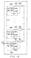
- the input terminal IN for the control signal voltage VCTRL is provided on a chip 1A.
- the chip 1A is provided with current generating circuit blocks 1000A to 1000N for the channels and functional circuit blocks 4001 to 400n for the channels.
- the current generating circuit blocks 1000A to 1000N for the channels receive the control signal voltage VCTRL which has been inputted through the input terminal IN to generate respective current outputs having desired current values and then supply the currents thus generated to the corresponding functional circuit blocks 4001 to 400n of the channels.
- the functional circuit blocks 4001 to 400n for the channels are operated in accordance with the currents thus supplied thereto.
- the current generating circuit blocks 1000A to 1000N include transistors 1001, and 1002 to 100n, input resistors 9001, and 9002 to 900n, input circuits 3001, and 3002 to 300n, and emitter resistors 2001, and 2002 to 200n, respectively, and generate currents in accordance with the control signal voltage VCTRL which has been inputted through the input terminal IN in order to supply the currents thus generated to the corresponding functional circuit blocks 4001 to 400n, respectively.
- the control signal voltage VCTRL is distributed from the input terminal IN through which the control signal voltage VCTRL is inputted to a plurality of current generating circuit blocks 1000A to 1000N through the respective control signal wirings
- the current generating circuit blocks 1000A to 1000N are arranged in the vicinities of the functional circuit blocks 4001 to 400n, respectively, and also the combined circuit blocks are arranged on the chip so as to be distributed thereon on the basis of a certain regulation.
- the current generating circuit blocks 1000A to 1000N include grounded-emitter npn transistors 1001 to 100n, respectively.
- control signal voltage VCTRL is supplied to the bases of the transistors 1001 to 100n, respectively, so that the transistors 1001 to 100n generate, in response to the control signal voltage thus supplied thereto, the currents in order to supply the currents to the corresponding functional circuit blocks 4001 to 400n.
- control signal voltage VCTRL is supplied to the bases of the transistors in the current generating circuit blocks 1000A to 1000N through the respective resistors 9001 to 900n which have different resistance values corresponding to the circuit blocks.
- the resistance values of the resistors 9001 to 900n which are connected to the bases of the transistors 1001 to 100n are selected in such a way that the differences between the voltage drops which are respectively developed across the resistors 9001 to 900n due to the base currents and the offset voltages in the grounding line to which the emitter resistors 2001 to 200n in the transistors 1001 to 100n are respectively connected match each other.
- the description will hereinbelow be given with respect to the operation of the present device having the above-mentioned configuration. That is, in the present invention shown in FIG. 10, though a plurality of current generating circuit blocks 1000A to 1000N are distributively arranged and the control signal voltage VCTRL is distributed from the input terminal IN to a plurality of current generating circuit blocks 1000A to 1000N through the respective control signal wirings, the current generating circuit blocks 1000A to 1000N are respectively arranged in the vicinities of the functional circuit blocks 4001 to 100n, and also the combined circuit blocks are arranged on the chip so as to be distributed thereon on the basis of the fixed regulation. Therefore, the resistance values of the grounding wirings between the channels can be quantitatively grasped.
- control signal voltage VCTRL is supplied to the bases of the transistors in the current generating circuit blocks 1000A to 1000N through the resistors which have the respective resistance values corresponding to the circuit blocks.
- the differences between the resistors 9001 to 900n which are respectively connected to the bases of the transistors 1001 to 100n are selected in such a way that the differences between the voltage drops which are developed across the resistors due to the base currents and the offset voltage differences between the reference ground point of the integrated circuit and the ground to which the emitter resistors are connected are substantially equal to one another.
- the offset voltage differences occurring in the grounding portions between the adjacent circuit blocks two by two have the ratio relationship of 11 : 9 : 7 : 5 : 3 : 1 in the direction from the center circuit block, out of the circuit blocks for a plurality of channels arranged on the chip, towards the end circuit block. Therefore, the resistance value of the resistor which is connected to the base of the transistor in the center circuit block may be suitably determined, and also the differences between the resistance values of the resistors which are connected to the bases of the transistors in the circuit blocks adjacent to each other may be determined so as to have the ratio relationship of 1 : 3 : 5 : 7 : 9 : 11 in the reverse order.
- the concrete proportional coefficients are determined on the basis of the resistance values of the ground wiring, the values of the currents flowing through the functional circuits, and the base currents.
- FIG. 12 shows the operation results in the case where the device is designed in such a way that instead of inputting directly the control voltage to the bases of the transistors of the current sources through the resistors, the control signal voltage is inputted to the bases of the transistors of the current sources through the resistors and the emitter-followers, whereby the voltage drops developed across the resistors are stabilized and also the temperature dependency of the output current is increased. It can be confirmed from FIG. 12 that for the three kinds of different output current values, the outputs for the 12 channels match approximately each other in the wide temperature range.
- the current output from the collector of the transistor in the current source is connected to the current input of the corresponding functional circuit block.
- the high frequency signal is provided on the output of the functional circuit block to which the collector output is connected, conversely, the high frequency signal is propagated to the collector so as to leak onto the control signal line through the collector to base junction capacitance which the transistor 1001 (or 1002, ..., 100n) has to generate the crosstalk.
- the crosstalk of the high frequency components is increased because of the capacitive coupling.
- a resistor 5001 (or 5002, ..., 500n) is inserted between the collector of the transistor 1001 (or 1002, ..., 100n) and the input of the functional circuit block 4001 (or 4002, ..., 400n) in order to increase the impedance, whereby the crosstalk can be suppressed to a fixed level or less.
- this insertion of the resistor offers, in addition to the effect of preventing the leakage of the high frequency components, the effect of attaining the isolation between the input and the output and also contributes to the suppression of the high frequency noises as well as the suppression of the oscillation.
- the large value is selected as long as the collector voltage of the transistor 1001 (or 1002, ..., 100n) is dropped by the voltage drop which is developed across the resistor 5001 (or 5002, ..., 500n) due to the current flowing therethrough and hence the transistor may not be saturated.
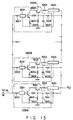
- a circuitry shown in FIG. 13 is an example in which the isolation between the constant current generating circuits and the functional circuit blocks is attained.
- the circuitry shown in FIG. 13 is designed in such a way that grounded-base transistor amplifiers 6001 (6002, ..., 600n) are respectively inserted between the collector outputs of the transistors 6001 to 600n in the current generating circuit blocks 1000A to 1000N for the channels and the inputs of the array functional circuit blocks 4001 to 400n having the corresponding channels in the current generating circuit blocks 1000A to 1000N.
- the circuitry shown in FIG. 13 follows the configuration shown in FIG. 10, in which the resistor 5001 (or 5002, ..., 500n) is connected in series with the input of the functional circuit block 4001 (or 4002, ..., 400n), as it is.
- the impedance is increased, thereby suppressing the crosstalk of the high frequency components to a fixed level or less.
- the voltage for the current generating circuit for controlling the constant currents which are supplied to the functional circuit blocks, respectively it is effective to use the voltage from the reference voltage generating circuit which is incorporated-on the same chip. This reason is that: since the ground line is distributed within the chip and hence its length is small, the influence of the chip current of the reference voltage is reduced; since no wiring is distributed in the outside of the IC and even if such a wiring is required, the scale of the wiring distribution is small, the influence of the noises is reduced; and since the overall chip is kept at the same temperature, for the change in the ambient air temperature, all the circuits are always subjected to the same temperature change and hence the temperature stability of the generated currents is improved, or it is possible to provide consciously the currents thus generated with the specific temperature characteristics.
- a diode is simply used as the means for generating a reference voltage which means is self-contained on the chip since the forward drop voltage thereof is utilized as the reference voltage.
- the forward drop voltage of the diode since the diode as the constituent element is made of the same material as that of the elements constituting the integrated circuit, if the diode is operated under the same condition as that in the elements of the integrated circuit, the same characteristics can be obtained for the diode at all times.
- the change in the base to emitter voltage of the transistor can be compensated by the voltage developed across one diode, and hence the simple circuitry can be obtained.
- the band gap reference voltage source (the band gap reference circuit) shown in FIG. 8A or 8B
- the circuit employing the band gap reference voltage source can be concretely applied to the laser driving circuit.
- the current generating circuit which is required for the circuit for driving the laser
- the driving current is changed in accordance with the temperature change so as to compensate therefor.
- the recent laser device for the optical interconnection has the lower threshold, and in addition thereto, the temperature characteristics of the threshold and the conversion efficiency have been considerably improved and also the recent laser has the characteristics in which the temperature dependency thereof is changed on the basis of a certain regulation. That is, for the circuit for generating the lasing threshold and the pulse driving current, instead of the circuit for generating a constant current in such a way as in the prior art, the circuit for changing the output current in accordance with a certain regulation in such a way as to compensate for the temperature characteristics of the semiconductor laser, i.e., the feedforward type circuit is effective.
- the temperature dependency of the control voltage which is to be inputted with the various output current values as parameters is just as we showed in FIG. 9.
- the reference voltage is obtained in which the temperature coefficient ranging from the positive range to the negative range and also the absolute values thereof matching each other can be generated with high accuracy.
- the input intensity of the semiconductor laser has a fixed value irrespective of the temperature.
- the active circuits or the low-pass filter circuits are respectively provided in the base input portions of the constant current generating circuits.
- the slight voltage differences occur between the ground line voltages of the circuits and hence any ground line voltage can not be necessarily regarded as the common ground voltage.
- the provision of the filter offers the effect of suppressing the high frequency random noises, it is not effective to the suppression of the noises, as the crosstalk between the channels, since the filter is not provided in the current path.
- the present invention is not limited to the bipolar transistor.
- the present invention is also applied to an active device such as a junction FET, a MOSFET, a GaAs MESFET, an HBT or a HEMT.
- the present invention since only one connection which is common to the array circuits is required for the power supply, the ground line and the control signal, the increase in the number of terminals necessary for the optical interconnect module package is suppressed so that the module configuration is simplified, and hence both the miniaturization and the promotion of low cost are made possible.
- the setting current values of all the channels can be adjusted to the same value by only adjusting one portion, and hence the convenience for use is improved. These effects contribute necessarily to the promotion of low cost at the system level.
Landscapes
- Engineering & Computer Science (AREA)
- Physics & Mathematics (AREA)
- Electromagnetism (AREA)
- General Physics & Mathematics (AREA)
- Radar, Positioning & Navigation (AREA)
- Automation & Control Theory (AREA)
- Amplifiers (AREA)
- Design And Manufacture Of Integrated Circuits (AREA)
Claims (28)
- Array-Vorrichtung mit Funktionsschaltungen für eine Mehrzahl von Kanälen, Konstantstrom-Erzeugungsschaltungen für die Mehrzahl von Kanälen zum Erzeugen von Konstantströmen, die verwendet werden, um die Funktionsschaltungen jeweils in Übereinstimmung mit einem von außerhalb gelieferten Steuersignal anzutreiben, und einer Verdrahtung zum Zuführen der Konstantströme von den Konstantstrom-Erzeugungsschaltungen an die jeweiligen Funktionsschaltungen, die auf einem integrierten Schaltungschip gebildet sind,
dadurch gekennzeichnet, daßdie Konstantstrom-Erzeugungsschaltungen (100A bis 100N), die so vorgesehen sind, daß sie den Kanälen entsprechen, in einem spezifischen Bereich auf dem integrierten Schaltungschip konzentriert angeordnet sind, unddie Verdrahtung sich aus einer gemeinsamen Verdrahtung zusammensetzt, die sich von einem in der Umgebung des spezifischen Bereichs vorgesehenen Anschluß zu den Umgebungen der Konstantstrom-Erzeugungsschaltungen (100A bis 100N) erstreckt. - Array-Vorrichtung gemäß Anspruch 1, dadurch gekennzeichnet, daß jede der Konstantstrom-Erzeugungsschaltungen (100A bis 100N) einen Transistor (10) mit geerdetem Emitter aufweist, der das Steuersignal als eine Basis-Ansteuereingabe empfängt.
- Array-Vorrichtung gemäß Anspruch 1, dadurch gekennzeichnet, daß jede der Konstantstrom-Erzeugungsschaltungen (100A bis 100N) aufweist:eine Eingangsschaltung (30) mit einem Eingangsanschluß, um durch diesen das Steuersignal zu empfangen; undeinen Transistor (10) mit geerdetem Emitter mit einer Basis, mit der ein Ausgangsanschluß der Eingangsschaltung (90) verbunden ist, und einen mit der zugeordneten Funktionsschaltung verbundenen Kollektor.
- Array-Vorrichtung gemäß Anspruch 3, dadurch gekennzeichnet, daß die Eingangsschaltung (30) eine aktive Schaltung aufweist.
- Array-Vorrichtung gemäß Anspruch 3, dadurch gekennzeichnet, daß die Eingangsschaltung (30) ein Tiefpaßfilter aufweist.
- Array-Vorrichtung gemäß Anspruch 1, dadurch gekennzeichnet, daß jede der Funktionsschaltungen eine Schaltung zum Ansteuern eines von einer Halbleiterlasereinrichtung emittierten Laserstrahls aufweist.
- Array-Vorrichtung gemäß Anspruch 1, ferner gekennzeichnet durch eine auf dem integrierten Schaltungschip angeordnete Bezugsspannungs-Erzeugungsschaltung, die zum Liefern einer Bezugsspannung an die Konstantstrom-Erzeugungsschaltungen (100A bis 100N).
- Array-Vorrichtung gemäß Anspruch 7, dadurch gekennzeichnet, daß die Bezugsspannungs-Erzeugungsschaltung eine Bandlücken-Konstantspannungsquelle aufweist.
- Array-Vorrichtung gemäß Anspruch 7, dadurch gekennzeichnet, daß die Bezugsspannungs-Erzeugungsschaltung eine interne Bezugsspannungs-Erzeugungsschaltung aufweist, und die interne Bezugsspannungs-Erzeugungsschaltung einem Vorwärtsspannungsabfall einer Diode entspricht, um einen Wert eines ausgegebenen Stroms mit einem spezifischen Temperaturkoeffizienten zu liefern.
- Array-Vorrichtung gemäß Anspruch 7, dadurch gekennzeichnet, daß die Bezugsspannungs-Erzeugungsschaltung eine Schaltung zum Ausgeben einer Spannung mit einem spezifischen Temperaturkoeffizienten aufweist.
- Array-Vorrichtung gemäß Anspruch 8, dadurch gekennzeichnet, daß die Bandlücken-Konstantspannungsquelle einen positiven/negativen Temperaturkoeffizienten aufweist.
- Array-Vorrichtung gemäß Anspruch 1, ferner gekennzeichnet durch zwischen den Konstantstrom-Erzeugungsschaltungen und den Funktionsschaltungen geschalteten Widerständen.
- Array-Vorrichtung gemäß Anspruch 1, ferner gekennzeichnet durch Transistorverstärker mit geerdeter Basis, die zwischen den Konstantstrom-Erzeugungsschaltungen (100A bis 100N) und den Funktionsschaltungen geschaltet sind.
- Array-Vorrichtung gemäß Anspruch 1, ferner gekennzeichnet durch Widerstände und Transistorverstärker mit geerdeter Basis, die zwischen den Konstantstrom-Erzeugungsschaltungen (100A bis 100N) und den Funktionsschaltungen geschaltet sind.
- Array-Vorrichtung mit Funktionsschaltungen für eine Mehrzahl von Kanälen, Konstantstrom-Erzeugungsschaltungen (100A bis 100N) für die Mehrzahl von Kanäle zum Erzeugen von Konstantströmen (100A bis 100N) die verwendet werden, um die Funktionsschaltungen jeweils in Übereinstimmung mit einem von außerhalb gelieferten Steuersignal anzusteuern, und einer Verdrahtung zum Zuführen der Konstantströme von den Konstantstromerzeugungsschaltungen (100A bis 100N) an die jeweiligen Funktionsschaltungen, die auf einem integrierten Schaltungschip gebildet sind,
dadurch gekennzeichnet, daß
die Konstantstrom-Erzeugungsschaltungen (100A bis 100N), die so vorgesehen sind, daß sie den Kanälen entsprechen, auf dem integrierten Schaltungschip regelmäßig angeordnet sind, und jede der Konstantstrom-Erzeugungsschaltungen (100A bis 100N) einen Transistor mit geerdetem Emitter, einen mit einer Basis des Transistors verbundenen Eingangswiderstand und einen mit einem Emitter des-Transistors verbundenen Emitter-Widerstand aufweist, und
die Verdrahtung sich aus einer gemeinsamen Verdrahtung zusammensetzt, die sich von einem Anschluß zu den Umgebungen der Konstantstrom-Erzeugungsschaltungen (100A bis 100N) erstreckt. - Array-Vorrichtung gemäß Anspruch 15, dadurch gekennzeichnet, daß die Konstantstrom-Erzeugungsschaltungen (100A bis 100N), die so vorgesehen sind, daß sie den Kanälen entsprechen, verteilt in den Umgebungen der Funktionsschaltungen in dem integrierten Schaltungschip angeordnet sind.
- Array-Vorrichtung gemäß Anspruch 15, dadurch gekennzeichnet, daß der Widerstandswert des Eingangswiderstands eingestellt ist, so daß er proportional zu der Differenz zwischen einer über dem Eingangswiderstand angelegten Spannung und der Massespannung der mit dem Emitter-Widerstand verbundenen Erdungsleitung ist.
- Array-Vorrichtung gemäß Anspruch 15, dadurch gekennzeichnet, daß der Widerstandswert des Eingangswiderstands auf eine solche Weise eingestellt ist, daß der Spannungsabfall, der sich über den Eingangswiderstand in Folge eines durch den Eingangswiderstand fließenden Basisstroms des Transistors entwickelt hat, mit der Offsetspannung der Erdungsleitung übereinstimmt, mit der der Emitterwiderstand verbunden ist.
- Array-Vorrichtung gemäß Anspruch 15, dadurch gekennzeichnet, daß die Widerstandswerte der Emitter-Widerstände in den Konstantstrom-Erzeugungsschaltungen (100A bis 100N) auf den gleichen Wert eingestellt sind.
- Array-Vorrichtung gemäß Anspruch 15, ferner gekennzeichnet durch Eingangsschaltungen (30), die zwischen den Eingangswiderständen der Konstantstrom-Erzeugungsschaltungen (100A bis 100N) und den Basis-Anschlüssen der Transistoren geschaltet sind.
- Array-Vorrichtung gemäß Anspruch 20, dadurch gekennzeichnet, daß die Eingangsschaltung (30) eine aktive Schaltung und/oder ein Bandpaßfilter aufweist.
- Array-Vorrichtung gemäß Anspruch 15, dadurch gekennzeichnet, daß jede der Funktionsschaltungen eine Schaltung zum Senden/Empfangen eines von einer Halbleiterlaservorrichtung emittierten Laserstrahls aufweist.
- Array-Vorrichtung gemäß Anspruch 15, ferner gekennzeichnet durch eine Bezugsspannungs-Erzeugungsschaltung, die auf dem integrierten Schaltungschip zum Liefern einer Bezugsspannung an die Konstantstrom-Erzeugungsschaltungen (100A bis 100N) angeordnet ist.
- Array-Vorrichtung gemäß Anspruch 23, dadurch gekennzeichnet, daß die Bezugsspannungs-Erzeugungsschaltung eine Bandlücken-Konstantspannungsquelle aufweist.
- Array-Vorrichtung gemäß Anspruch 23, dadurch gekennzeichnet, daß die Bezugsspannungs-Erzeugungsschaltung eine interne Bezugsspannungs-Erzeugungsquelle aufweist, und die interne Bezugsspannungs-Erzeugungsquelle einem Vorwärtsspannungsabfall einer Diode entspricht, um einen Wert eines ausgegebenen Stroms mit einem spezifischen Temperaturkoeffizienten zu liefern.
- Array-Vorrichtung gemäß Anspruch 23, dadurch gekennzeichnet, daß die Bezugsspannungs-Erzeugungsschaltung eine Schaltung zum Ausgeben einer Spannung mit einem spezifischen Temperaturkoeffizienten aufweist.
- Array-Vorrichtung gemäß Anspruch 15, dadurch gekennzeichnet, daß die Bandlücken-Konstantspannungsquelle einen positiven/negativen Temperaturkoeffizienten aufweist.
- Array-Vorrichtung gemäß Anspruch 15, ferner gekennzeichnet durch Schaltungen, die jeweils zwischen den Konstantstrom-Erzeugungsschaltungen (100A bis 100N) und den Funktionsschaltungen geschaltet sind, und jede sich aus einem Widerstand und/oder Transistorverstärker mit geerdeter Basis zusammensetzt.
Applications Claiming Priority (6)
| Application Number | Priority Date | Filing Date | Title |
|---|---|---|---|
| JP07619796A JP3313571B2 (ja) | 1996-03-29 | 1996-03-29 | アレイ素子用電流発生回路 |
| JP7619696A JP3313570B2 (ja) | 1996-03-29 | 1996-03-29 | アレイ素子用電流発生回路 |
| JP7619796 | 1996-03-29 | ||
| JP76196/96 | 1996-03-29 | ||
| JP76197/96 | 1996-03-29 | ||
| JP7619696 | 1996-03-29 |
Publications (2)
| Publication Number | Publication Date |
|---|---|
| EP0798618A1 EP0798618A1 (de) | 1997-10-01 |
| EP0798618B1 true EP0798618B1 (de) | 2002-02-20 |
Family
ID=26417347
Family Applications (1)
| Application Number | Title | Priority Date | Filing Date |
|---|---|---|---|
| EP97302193A Expired - Lifetime EP0798618B1 (de) | 1996-03-29 | 1997-03-27 | Array-Anordnung mit Schaltkreisen und Konstantstromquellen für eine Vielzahl von Kanälen |
Country Status (3)
| Country | Link |
|---|---|
| US (1) | US5883546A (de) |
| EP (1) | EP0798618B1 (de) |
| DE (1) | DE69710506T2 (de) |
Cited By (1)
| Publication number | Priority date | Publication date | Assignee | Title |
|---|---|---|---|---|
| CN109781388A (zh) * | 2019-02-25 | 2019-05-21 | 电子科技大学中山学院 | 基于分布式恒流驱动电源单管大功率激光器筛选测试系统 |
Families Citing this family (6)
| Publication number | Priority date | Publication date | Assignee | Title |
|---|---|---|---|---|
| DE19635050A1 (de) * | 1996-08-30 | 1998-03-05 | Philips Patentverwaltung | Schaltungsanordnung mit wenigstens zwei Signalpfaden |
| JP2001127366A (ja) | 1999-10-25 | 2001-05-11 | Toshiba Corp | 固体レーザ装置の出力制御方法、固体レーザ用電源装置及び固体レーザ装置 |
| JP2003150115A (ja) * | 2001-08-29 | 2003-05-23 | Seiko Epson Corp | 電流生成回路、半導体集積回路、電気光学装置および電子機器 |
| US7436242B1 (en) * | 2005-01-13 | 2008-10-14 | National Semiconductor Corporation | System and method for providing an input voltage invariant current source |
| WO2011107160A1 (en) | 2010-03-05 | 2011-09-09 | Epcos Ag | Bandgap reference circuit and method for producing the circuit |
| CN103383585B (zh) * | 2013-07-10 | 2015-01-07 | 电子科技大学 | 一种宽输入范围超低温漂带隙基准电压源 |
Family Cites Families (9)
| Publication number | Priority date | Publication date | Assignee | Title |
|---|---|---|---|---|
| US3978473A (en) * | 1973-05-01 | 1976-08-31 | Analog Devices, Inc. | Integrated-circuit digital-to-analog converter |
| US4967192A (en) * | 1987-04-22 | 1990-10-30 | Hitachi, Ltd. | Light-emitting element array driver circuit |
| US5122686A (en) * | 1991-07-18 | 1992-06-16 | Advanced Micro Devices, Inc. | Power reduction design for ECL outputs that is independent of random termination voltage |
| EP0584634B1 (de) * | 1992-08-17 | 1995-12-20 | Alcatel SEL Aktiengesellschaft | Schaltung zur Amplitudenmodulation des Ansteuersignals eines Lasers |
| US5398008A (en) * | 1992-08-17 | 1995-03-14 | Alcatel N.V. | Circuit arrangement for amplitude-modulating the drive signal of a laser |
| JPH06308902A (ja) * | 1993-02-26 | 1994-11-04 | Mitsubishi Electric Corp | 半導体集積回路及び表示装置 |
| US5448208A (en) * | 1993-07-15 | 1995-09-05 | Nec Corporation | Semiconductor integrated circuit having an equal propagation delay |
| US5432358A (en) * | 1994-03-24 | 1995-07-11 | Motorola, Inc. | Integrated electro-optical package |
| DE69525865T2 (de) * | 1994-04-22 | 2002-09-19 | Canon Kk | Treiberschaltung für eine Leuchtdiode |
-
1997
- 1997-03-27 US US08/828,778 patent/US5883546A/en not_active Expired - Fee Related
- 1997-03-27 EP EP97302193A patent/EP0798618B1/de not_active Expired - Lifetime
- 1997-03-27 DE DE69710506T patent/DE69710506T2/de not_active Expired - Fee Related
Cited By (1)
| Publication number | Priority date | Publication date | Assignee | Title |
|---|---|---|---|---|
| CN109781388A (zh) * | 2019-02-25 | 2019-05-21 | 电子科技大学中山学院 | 基于分布式恒流驱动电源单管大功率激光器筛选测试系统 |
Also Published As
| Publication number | Publication date |
|---|---|
| EP0798618A1 (de) | 1997-10-01 |
| DE69710506D1 (de) | 2002-03-28 |
| US5883546A (en) | 1999-03-16 |
| DE69710506T2 (de) | 2002-10-24 |
Similar Documents
| Publication | Publication Date | Title |
|---|---|---|
| US6122085A (en) | Lightwave transmission techniques | |
| EP1276230B1 (de) | Kaskodenkettenverstärker | |
| EP0839407B1 (de) | Begrenzender hochfrequenz-differenz-kettenverstärker | |
| US20100183318A1 (en) | Laser diode driver with back terminator and optical transmitter providing the same | |
| EP0895325A2 (de) | Temperaturabhängiger Konstantstromschaltkreis und eine diesen verwendende Treiberschaltung für lichtemittierende Halbleiterelemente | |
| US7035302B2 (en) | Optical transmission module | |
| EP0504308B1 (de) | Fiberoptischer Transimpedanz Empfänger | |
| US7764885B2 (en) | Asymmetric rise/fall time and duty cycle control circuit | |
| EP0798618B1 (de) | Array-Anordnung mit Schaltkreisen und Konstantstromquellen für eine Vielzahl von Kanälen | |
| US6792019B2 (en) | Driver with tail currents in discrete subranges | |
| US7006543B2 (en) | System and circuit for a multi-channel optoelectronic device driver | |
| CA2203489C (en) | Circuit in cmos technology for high speed driving of optical sources | |
| US5386109A (en) | Pre-amplifier for optical receiving and optical receiver using the same | |
| US6606177B1 (en) | Driver circuit and optical-transmission module | |
| JP3313570B2 (ja) | アレイ素子用電流発生回路 | |
| JP3313571B2 (ja) | アレイ素子用電流発生回路 | |
| US5343323A (en) | Lan electro-optical interface | |
| WO1988002575A1 (en) | Amplifier | |
| US20100289594A1 (en) | Modulator driver circuit having chirped components | |
| US8018286B2 (en) | Low power integrated circuit | |
| US20240007069A1 (en) | Hybrid distributed driver | |
| EP1236294A2 (de) | Vorverzerrungsschaltung zweiter ordnung für laserdiode | |
| US6972620B2 (en) | Post amplifier array integrated circuit | |
| JP2000059318A (ja) | 光伝送モジュール |
Legal Events
| Date | Code | Title | Description |
|---|---|---|---|
| PUAI | Public reference made under article 153(3) epc to a published international application that has entered the european phase |
Free format text: ORIGINAL CODE: 0009012 |
|
| 17P | Request for examination filed |
Effective date: 19970423 |
|
| AK | Designated contracting states |
Kind code of ref document: A1 Designated state(s): DE FR SE |
|
| 17Q | First examination report despatched |
Effective date: 20000508 |
|
| GRAG | Despatch of communication of intention to grant |
Free format text: ORIGINAL CODE: EPIDOS AGRA |
|
| GRAG | Despatch of communication of intention to grant |
Free format text: ORIGINAL CODE: EPIDOS AGRA |
|
| GRAH | Despatch of communication of intention to grant a patent |
Free format text: ORIGINAL CODE: EPIDOS IGRA |
|
| GRAH | Despatch of communication of intention to grant a patent |
Free format text: ORIGINAL CODE: EPIDOS IGRA |
|
| GRAA | (expected) grant |
Free format text: ORIGINAL CODE: 0009210 |
|
| AK | Designated contracting states |
Kind code of ref document: B1 Designated state(s): DE FR SE |
|
| REF | Corresponds to: |
Ref document number: 69710506 Country of ref document: DE Date of ref document: 20020328 |
|
| ET | Fr: translation filed | ||
| PLBE | No opposition filed within time limit |
Free format text: ORIGINAL CODE: 0009261 |
|
| STAA | Information on the status of an ep patent application or granted ep patent |
Free format text: STATUS: NO OPPOSITION FILED WITHIN TIME LIMIT |
|
| 26N | No opposition filed |
Effective date: 20021121 |
|
| PGFP | Annual fee paid to national office [announced via postgrant information from national office to epo] |
Ref country code: SE Payment date: 20090306 Year of fee payment: 13 Ref country code: DE Payment date: 20090319 Year of fee payment: 13 |
|
| PGFP | Annual fee paid to national office [announced via postgrant information from national office to epo] |
Ref country code: FR Payment date: 20090316 Year of fee payment: 13 |
|
| EUG | Se: european patent has lapsed | ||
| REG | Reference to a national code |
Ref country code: FR Ref legal event code: ST Effective date: 20101130 |
|
| PG25 | Lapsed in a contracting state [announced via postgrant information from national office to epo] |
Ref country code: FR Free format text: LAPSE BECAUSE OF NON-PAYMENT OF DUE FEES Effective date: 20100331 |
|
| PG25 | Lapsed in a contracting state [announced via postgrant information from national office to epo] |
Ref country code: DE Free format text: LAPSE BECAUSE OF NON-PAYMENT OF DUE FEES Effective date: 20101001 |
|
| PG25 | Lapsed in a contracting state [announced via postgrant information from national office to epo] |
Ref country code: SE Free format text: LAPSE BECAUSE OF NON-PAYMENT OF DUE FEES Effective date: 20100328 |