EP0797121A2 - Exposure apparatus - Google Patents
Exposure apparatus Download PDFInfo
- Publication number
- EP0797121A2 EP0797121A2 EP97104531A EP97104531A EP0797121A2 EP 0797121 A2 EP0797121 A2 EP 0797121A2 EP 97104531 A EP97104531 A EP 97104531A EP 97104531 A EP97104531 A EP 97104531A EP 0797121 A2 EP0797121 A2 EP 0797121A2
- Authority
- EP
- European Patent Office
- Prior art keywords
- light
- recessed portion
- pitch
- exposure
- protruded portion
- Prior art date
- Legal status (The legal status is an assumption and is not a legal conclusion. Google has not performed a legal analysis and makes no representation as to the accuracy of the status listed.)
- Granted
Links
Images


Classifications
-
- G—PHYSICS
- G03—PHOTOGRAPHY; CINEMATOGRAPHY; ANALOGOUS TECHNIQUES USING WAVES OTHER THAN OPTICAL WAVES; ELECTROGRAPHY; HOLOGRAPHY
- G03F—PHOTOMECHANICAL PRODUCTION OF TEXTURED OR PATTERNED SURFACES, e.g. FOR PRINTING, FOR PROCESSING OF SEMICONDUCTOR DEVICES; MATERIALS THEREFOR; ORIGINALS THEREFOR; APPARATUS SPECIALLY ADAPTED THEREFOR
- G03F7/00—Photomechanical, e.g. photolithographic, production of textured or patterned surfaces, e.g. printing surfaces; Materials therefor, e.g. comprising photoresists; Apparatus specially adapted therefor
- G03F7/70—Microphotolithographic exposure; Apparatus therefor
- G03F7/70216—Mask projection systems
- G03F7/7035—Proximity or contact printers
-
- G—PHYSICS
- G03—PHOTOGRAPHY; CINEMATOGRAPHY; ANALOGOUS TECHNIQUES USING WAVES OTHER THAN OPTICAL WAVES; ELECTROGRAPHY; HOLOGRAPHY
- G03F—PHOTOMECHANICAL PRODUCTION OF TEXTURED OR PATTERNED SURFACES, e.g. FOR PRINTING, FOR PROCESSING OF SEMICONDUCTOR DEVICES; MATERIALS THEREFOR; ORIGINALS THEREFOR; APPARATUS SPECIALLY ADAPTED THEREFOR
- G03F7/00—Photomechanical, e.g. photolithographic, production of textured or patterned surfaces, e.g. printing surfaces; Materials therefor, e.g. comprising photoresists; Apparatus specially adapted therefor
- G03F7/70—Microphotolithographic exposure; Apparatus therefor
- G03F7/70408—Interferometric lithography; Holographic lithography; Self-imaging lithography, e.g. utilizing the Talbot effect
Landscapes
- Physics & Mathematics (AREA)
- General Physics & Mathematics (AREA)
- Preparing Plates And Mask In Photomechanical Process (AREA)
- Exposure And Positioning Against Photoresist Photosensitive Materials (AREA)
- Projection-Type Copiers In General (AREA)
Abstract
Description
- The present invention relates to an equipment for exposing fine cycling patterns.
- With respect to conventional techniques, for example, there is a projection exposure equipment in P. 690 of Micro Optics Handbook (edited by the Applied Physics Society, Asakura Shoten Publishing Company, 1995), and referring to this equipment, the technique is described. FIG. 1 shows a configuration of a conventional exposure equipment. The beam from a
light source 14 is converted to a proper beam by a beam compressor 15 (or beam expander) and impinges on ahomogenizer 16. Thehomogenizer 16 comprises 3 to 6 mm square lens arrays, and homogenizes illuminance distribution of the lighting system as well as forms thesecondary light source 17 in the vicinity of exit end face. The light from thesecondary light source 17 illuminates areticle 19 with an exposure pattern drawn by alighting lens 18 and forms image on theexposure surface 22 with animage forming lens 20. In this event, the image of thesecondary light source 17 is formed on theentrance pupil surface 21. - The resolution R of this conventional exposure equipment can be expressed by the following equation with the wavelength of illuminating light designated by λ and the number of apertures of the image-formation optical system by NA (Numerical Aperture):

- where, k1 is a constant determined from exposure/development process conditions, and, in general, takes the value about 0.5 to 0.8.
- In the meantime, the depth of a focus Z of the image-formation optical system is given by the following equation:

- Wavelength λ is unequivocally determined by the type of light source, and in general, 435 nm (g ray) or 365 nm (i ray) is used. It is the simplest method for improving the resolution to further shorten wavelengths of the light source, or it is possible to improve the resolution by adopting NA with a high value. However, because higher NA shallows the depth of a focus based on Eq. (2) and eliminates an error allowance of the exposure position, it is restricted to more or less 0.5 to 0.6. Consequently, the resolution R of the conventional exposure equipment is restricted to about 1.6λ in terms of pitch with k1 = 0.5, NA = 0.6. A technique called a phase shift method is proposed to improve this resolution limit (P. 694 of the Micro-optics Handbook). In this proposal, a phase shifter is formed on the reticle for improving the resolution in the conventional exposure equipment. FIG. 2(A) and FIG. 2(B) show a principle of the phase shift method in the conventional exposure equipment. The
reticle 19 in the conventional method is formed with atransparent base plate 19a and amask 19b, where the light amplitude on the exposure surface is denoted withnumeral 23 and light intensity with 24. As against this, in the phase shift method, aphase shifter 19c is formed in every other clearance between masks, and by delaying the phase of light passing thephase shifter 19c by π, we can have the light amplitude and light intensity shown with 23a, 24a on the exposure surface, and the contrast is able to be improved as compared to the conventional method. There is also a method which does not use amask 19b, whose working principle is shown in FIG. 3. In this event, thereticle 19 comprises atransparent substrate 19a andphase shifter 19c. Thephase shifter 19c is able to achieve light amplitude and light intensity shown in 23b and 24b on the exposure surface by delaying by π the light phase passing thephase shifter 19c, enabling improvement of the contrast. - In the conventional exposure equipment as described above, following problems are found irrespective of the presence of the
phase shifter 19c or not. - Now referring to an exposure equipment with higher resolution to which a
phase shifter 19c is mounted, such problems will be described in detail. - That is, in this case, according to the principle shown in FIG. 3, the cycle of
light intensity 24b on the exposure surface is one half that of thephase shifter 19c on the reticle, and by the adoption of the phase shift method, the resolution of the exposure equipment should be doubled. However, in actuality, because the image-forming optical system intervenes between thereticle 19 and the exposure surface, the resolution according to the theory is unable to be obtained. - The reasons are shown as follows. That is, FIG. 4 shows the optical path of the light penetrating the reticle with a phase shifter. Light 25 (wavelength λ) impinging on the
reticle 19 separates into the beam that penetrates as it is by penetrating thephase shifter 19c (zero-order beam) and diffracted beam (± first order beam). Let the cycle of thephase shifter 19c be Λ, the diffraction angle θ of diffracted beam is given by the following equation:
- These penetration and diffraction beams impinge on the
image forming lens 20, and form images on thepupil surface 21 as shown in 26, 26A, and 26B, respectively. The image-forming point of the zero-order beam is located on theoptical axis 27, but since the ± first-order beam is tilted by θ in the traveling direction with respect to theoptical axis 27, the image is formed at the position "b" away from the optical axis. Because the size of "b" is proportional to sin θ, if the cycle Λ becomes smaller than a certain value, the image forming point of the ± first-order beam is located outside the aperture of the pupil surface (b > a) and the light is shielded in the area outside the aperture of the pupil. Because the projected pattern on the exposure surface is formed by the light penetrating thepupil surface 21, shielding part of the penetrating light results in degradation of resolution of the projected pattern. - Based on the foregoing, the effects of the phase shift method is restricted to at most 30 to 40% improvement in resolution. That is, if the resolution of the exposure equipment is expressed by substituting the pitch of the projected pattern formed on the
exposure surface 22, it is said that it would be limited to formation of about 1.2 λ pitch. - Degradation of the resolution described above is essentially generated irrespective of presence of the
phase shifter 19c, and if thephase shifter 19c is not used, the resolution further degrades. - Under these conditions, the present invention is to provide an exposure equipment of high resolution which has simple construction and can expose fine patterns whose exposure pattern pitch is λ (wavelength of light source) or smaller, and is designed to have the following configuration in order to solve the above-mentioned problems.
- The present invention is an exposure equipment which comprises a laser beam source, an expanding means for expanding laser beams of wavelength λ outgoing from the laser beam source and forming it into plane wave of parallel, beams, a plate-form member formed with transparent material with refraction index n, and an exposure substrate located close to the plate-form member on the surface of which sensitized film is formed, wherein on the surface of the plate-form member facing against the exposure substrate side, recessed portion and protruded portion are repeatedly formed, and allowing the plane wave expanded by the expanding means to penetrate the recessed portion or protruded portion generates a ± first order diffracted light, and the sensitized film is located at the position in which the + first order diffracted light and the - first order diffracted light intersect each other, fringes generated by interference between the diffracted lights exposes the sensitized film.
- According to the above-mentioned configuration, in the present invention, fringes with a pitch one half that of the said recessed or protruded portion are formed with good contrast on the sensitized film, and an exposure equipment with high resolution can be realized.
- The present invention is an exposure equipment which comprises the recessed portion or protruded portion covered with a transparent layer of refraction index n0 (where, n0 > n) and the film thickness of the transparent layer which is greater than a pitch of the recessed portion or protruded portion.
- With this configuration, it is possible to suppress generation of diffracted light of ± second-order or higher.
- The present invention is an exposure equipment which comprises a laser beam source, an expanding means for expanding laser beams of wavelength λ outgoing from the laser beam source and forming it into plane wave of parallel beams, a plate-form member formed with transparent material with refraction index n, and an exposure substrate located close to the plate-form member on the surface of which sensitized film is formed, wherein on the surface of the plate-form member facing against the exposure substrate side, recessed portion and protruded portion are repeatedly formed, and allowing the plane wave expanded by the expanding means to penetrate the recessed portion or protruded portion generates a zero order and ± first order to ±q order (q ≥ 1) diffracted lights, and ratio of sum of light quantity of even order diffracted lights of these lights to sum of light quantity of odd order diffracted lights of these lights ranges from 0.5 to 2.0, the sensitized film is located at the position in which these diffracted lights intersect one another, fringes generated by interference between the diffracted lights exposes the sensitized film.
-
- FIG. 1 is a schematic representation of a conventional exposure equipment;
- FIG. 2(A) and FIG. 2(B) are diagrams showing the working principle of the phase shift method in the conventional exposure equipment;
- FIG. 3 is a diagram showing the working principle of the other phase shift method in the conventional exposure equipment;
- FIG. 4 is a diagram showing an optical path of the light penetrating a reticle with a phase shifter in the conventional exposure equipment;
- FIG. 5 is a schematic representation of an exposure equipment according to the first embodiment of the present invention;
- FIG. 6 is a section view of a phase shifter of the exposure equipment according to the first embodiment of the present invention;
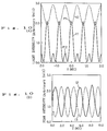
- FIG. 7 (A) and FIG. 7 (B) are first illustrative diagrams showing the characteristics of light intensity distribution on the sensitized film of the exposure equipment according to the first embodiment of the present invention;
- FIG. 8 (A) and FIG. 8 (B) are second illustrative diagrams showing the characteristics of light intensity distribution on the sensitized film of the exposure equipment according to the first embodiment of the present invention;
- FIG. 9 (A) and FIG. 9 (B) are third illustrative diagrams showing the characteristics of light intensity distribution on the sensitized film of the exposure equipment according to the first embodiment of the present invention;
- FIG. 10 (A) and FIG. 10 (B) are fourth illustrative diagrams showing the characteristics of light intensity distribution on the sensitized film of the exposure equipment according to the first embodiment of the present invention;
- FIG. 11 is a diagram illustrating the principle showing the relationship between the cycle of the cyclic condition and the cycle of the exposure pattern of the exposure equipment according to the embodiment of the present invention;
- FIG. 12 is a diagram showing the optical path of the light penetrating the cyclic recessed and protruded constructions of a trapezoidal cross section according to the second embodiment of this invention;
- FIG. 13 is a diagram showing the optical path of the light penetrating the cyclic recessed and protruded constructions of a trapezoidal cross section according to the third embodiment of this invention; and
- FIG. 14 is a diagram showing the distribution of light intensity on the sensitized film of the exposure equipment according to an embodiment of this invention.
-
- 1 ... laser beam source,
- 2 ... laser beam
- 3a, 3b ... reflection mirror,
- 4 ... beam expander optical system
- 4a ... focusing lens,
- 4b ... collimator lens,
- 4c ... pinhole
- 5 ... parallel beam,
- 6 ... phase shifter,
- 6a ... cyclic rugged structure,
- 7 ... spacer,
- 8 ... sensitized film
- 9 ... exposure substrate
- Referring now to FIG. 5 to FIG. 11, there is shown the first embodiment of this invention. FIG. 5 shows a construction of the exposure equipment according to the embodiment of this invention, which comprises a
laser beam source 1, reflectingmirror optical system 4,phase shifter 6, spacer 7, andexposure substrate 9. In FIG. 5, laser beam 2 (wave length λ) impinging from alight source 1, such as Ar laser, He-Cd laser, etc. reflects amirror optical system 4. - The beam expander
optical system 4 comprises a focusinglens 4a,collimator lens 4b, andpinhole 4c, wherein laser beam is converged by a focusinglens 4a, passes through thepinhole 4c located on the focal plane of the focusinglens 4a, and is converted toparallel beam 5 with the beam diameter expanded by thecollimator lens 4b. In this event, thepinhole 4c works to remove speckle noise of laser. Theparallel beam 5 of plane wave vertically impinges on and penetrates the parallel flat plateshape phase shifter 6 formed with transparent material with the refraction index n. - The outgoing surface side of the
phase shifter 6 has the cyclicrugged structure 6a in depth
- On the surface of the
exposure substrate 9, sensitizedfilm 8 is laminated, and on this sensitized film, the ± first-order diffraction light interferes with each other to form fringes at fine pitches and expose the sensitized film. Thesensitized film 8 opposes to thephase shifter 6 via the spacer 7, and a clearance equivalent to the thickness of the spacer 7 exists between thecyclic construction face 6a and sensitizedfilm 8. - FIG. 6 shows a cross sectional view of the phase shifter of the exposure equipment according to the first embodiment of the present invention.
- As shown in FIG. 6, let the pitch of the cyclic
rugged structure 6a be Λ and the depth h, give the width of the protruded portion with εΛ if the rugged structure is a rectangle, set the origin at the position a distance z from the center of the cyclic construction surface along the normal direction, and consider the coordinate axis in the direction passing the origin O and along the grating vector (vector crossing at right angles in the grating direction). - FIG. 7(A), FIG. 7(B) is the first illustrative diagram showing the characteristics of light intensity distribution on the sensitized film of the exposure equipment according to the first embodiment of this invention, indicating the computation results when analysis is made with λ = 0.4579 µm and the rugged structure assumed to be a rectangle of Λ = 0.8 µm,

- FIG. 7(A) shows the light intensity distribution along the x coordinate. In spite of the pitch of the
rugged structure 10 being 0.8 µm, a half pitch (0.4 µm pitch)intensity distribution pattern 11 is obtained. Therugged structure 10 schematically shows the cyclicrugged structure 6a shown in FIG. 6 for convenience of description and is drawn with a dotted line to scale of abscissa of FIG. 7(A). For the same effect, in FIG. 8 (A)-FIG. 10(A), therugged structure 10 shown in a dotted line is drawn. - FIG. 7(B) plots the relation of the light intensity P1 at the intensity distribution x = 0 µm and light intensity P2 in x = -0.4 µm to the distance z, and a
solid line 12 corresponds to the light intensity P1 and a broken line to the light intensity P2. Both have a slight waviness due to influence of boundary diffraction wave generated at the start/end line position (boundary line rugged structure 6a shown in FIG. 6) in the x-axis direction of the rugged structure, but generally do not lean to z but provide an equally uniform value. - That is, even if there is an error in the position of the sensitized film 8 (clearance equivalent to the thickness of spacer 7), there is no degradation in the intensity distribution pattern, and contrast of exposure is satisfactory. Consequently, position setting of the exposure substrate is not necessarily carried out by an expensive high-accuracy stepper used for the semiconductor process, and positioning achieved by just inserting the spacer 7 for pressing as described in this embodiment is enough.
- FIG. 8(A), FIG. 8(B) is the second illustrative diagram showing the characteristics of the light intensity distribution on the sensitized film of the exposure equipment according to the first embodiment of this invention, indicating the computation results when analysis is made with λ = 0.4579 µm and the rugged structure assumed to be a rectangle of Λ = 0.8 µm,

- FIG. 8(A) shows the light intensity distribution along the x coordinate. In spite of the pitch of the
rugged structure 10 being 0.8 µm, a half pitch (0.4 µm pitch)intensity distribution pattern 11 is obtained, but since the duty ratio ε of therugged structure 10 deviates from 0.5, a difference is generated between the light intensity P1 at x = 0 µm and the light intensity P2 at x = -0.4 µm. - FIG. 8(B) plots the relation of these light intensities P1 and P2 to the distance z, and a
solid line 12 corresponds to the light intensity P1 and abroken line 13 to the light intensity P2. Both have a slight waviness of reverse phase dependent on z, but the intensity ratio is around 1.0 : 0.6 even under the worst conditions. - FIG. 9(A), FIG. 9(B) is the third illustrative diagram showing the characteristics of the light intensity distribution on the sensitized film of the exposure equipment according to the first embodiment of this invention, indicating the computation results when analysis is made with λ = 0.4579 µm and the rugged structure assumed to be a rectangle of Λ = 0.8 µm,

- FIG. 9(A) shows the light intensity distribution along the x coordinate. In spite of the pitch of the
rugged structure 10 being 0.8 µm, a half pitch (0.4 µm pitch)intensity distribution pattern 11 is obtained, but since the depth of therugged structure 10 deviates from
- FIG. 9(B) plots the relation of these light intensities P1 and P2 to the distance z, and a
solid line 12 corresponds to the light intensity P1 and abroken line 13 to the light intensity P2. Both light intensity P1 and P2 have a waviness of reverse phase dependent on z, and the intensity ratio is around 1.0 : 0.4 even under the worst conditions. - FIG. 10(A), FIG. 10(B) are fourth illustrative diagrams showing the characteristics of light intensity distribution on the sensitized film of the exposure equipment according to the first embodiment of this invention, indicating the computation results of analysis with λ = 0.4579 µm and rugged structure assumed to be a sine wave profile of Λ = 0.8 µm,

- FIG. 10(A) shows the light intensity distribution along the x coordinate. As in the case of FIG. 7, in spite of the pitch of the
rugged structure 10 being 0.8 µm, a half pitch (0.4 µm pitch)intensity distribution pattern 11 is obtained, but since the cross-sectional profile of therugged structure 10 deviates from the rectangular profile, a large difference is generated between the light intensity P1 at x = 0 µm and the light intensity P2 at x = -0.4 µm. - FIG. 10(B) plots the relation of these light intensities P1 and P2 to the distance z, and a
solid line 12 corresponds to the light intensity P1 and abroken line 13 to the light intensity P2. Both light intensity P1 and P2 have a large waviness of reverse phase dependent on z, and the intensity ratio is around 1.0 : 0.15 under the worst conditions. - When allowance for error of the exposure substrate position is considered, as is clear from FIG. 7(A)-FIG. 10(B), in order to optimize the exposure contrast, it is preferable that the cross-sectional profile of the rugged structure should be a rectangle of


- Now, FIG. 11 is an illustrative drawing that describes the principle showing the relationship between the pitch of the recessed portion or protruded portion on the
phase shifter 6 and the pitch of the exposure pattern in the exposure equipment according to the first embodiment of this invention. That is, referring to the drawing, the relationship between the pitch of the recessed portion or protruded portion and the pitch of the exposure pattern will be described in detail. - The
light 5 of wavelength λ which vertically impinges on thecyclic structure surface 6a of the phase shifter is diffracted after penetrating the cyclic structure, and ± first-order diffracted light 5A, 5B are generated. Let the pitch of the cyclic structure at the position Q1 on thecyclic structure surface 6a denote Λ1, and the pitch of the cyclic structure at the position of point

- If the diffracted light of + first order diffracted at point Q1 and the diffracted light of - first order diffracted at point Q2 intersect at point Q12 on the
exposure surface 8, based on the principle of two beam interference, fringes are formed on the point Q12. The position of the point

- And the pitch Λ12 of fringes at point Q12 is given by the following equation from Eq. (4) and Eq. (5):

- Consequently, in the case of uniform pitch, for (


cyclic structure 6a is obtained. Because as long as Λ1 ≤ λ and Λ2 ≤ λ, diffracted light is generated, it is possible to achieve Λ12 ≥ λ/2 for the minimum pitch of the intensity distribution pattern (limit of resolution). That is, resolution more than double that of the exposure equipment in the conventional example can be obtained. - When the pitch varies to positions


- Consequently, if Δ << 1 (the relation of Δ << 1 sufficiently holds for if the exposure position approximates to the cyclic structure surface), the following equation holds for from


- On the other hand, if Δ << 1, from Eq. (7), the pitch Λ12 of fringes can be approximated to the following equation:

- Consequently, the pitch Λ12 of fringes corresponds to one half the pitch Λ3 of the cyclic structure at the position on the cyclic structure surface corresponding to it, and even when the pitch varies to positions, the relationship of one-half pitch is accurately observed. In this way, in the exposure equipment according to the conventional example, a high-accuracy image forming lens is required for projecting the exposure pattern on the reticle onto the exposure surface free from any distortion, but in the present embodiment, only approximating the exposure position to the cyclic structure surface (that is, the structure surface on which the recessed portion and the protruded portion are repeatedly formed by a specified pitch on a flat plate) enables one-half pitch patterning free from distortion.
- If it is only in the area where two beams intersect each other that fringes are formed on the
exposure surface 8 and if the intersection of the diffracted lights generated from the start point A and the end point B of the cyclic structure is denoted as C, exposure is limited to the area which is surrounded by a triangle ABC and is approximated to the cyclic structure. - Because interference at point Q12 takes place among a plurality of beams if the light penetrating the
cyclic structure surface 6a contains zero-order light (component which penetrates without diffraction) and light of other orders, contrast of fringes degrade and the contrast also relates to the position of the exposure surface. It is because no diffracted light other than ± first order is generated that fringes with good contrast were obtained in the example of FIG. 7, as described below. In general, if the intensity of nth-order diffracted light generated by penetrating the phase shifter with a rectangular cross section shown in FIG. 6 be In, the intensity ratio of each diffracted light can be given by the following equation.

- Under the conditions of FIG. 7(A) and FIG. 7(B)

- On the other hand, under the conditions of FIG. 8(A) and FIG. 8(B)

- As described above, in order to obtain fringes with good contrast irrespective of the exposed surface position, the small ratio of the zero-order light quantity to the total diffracted light quantity (for example, I0/(I0 + 2I1) ≤ 0.1) is essential.
- Now, the second embodiment according to this invention will be described in detail.
- Because the second embodiment is exactly same as the first embodiment with only exception that the cyclic width of the cyclic structure, that is the pitch Λ of the recessed or protruded portion is limited to λ < Λ < 2λ, the same drawings used as in the case of the first embodiment are referred and overlapping description will be omitted.
- In the first embodiment, the cross section of the periodic rugged structure was a rectangle, but in actuality, at the rugged boundary, sagging occurs, and the cross section becomes, for example, a trapezoidal cross section as shown in FIG. 12. In FIG. 12, the light a, b impinging on the bottom surface PQ of the recessed portion and the top surface RS of the protruded portion of the phase shifter penetrates the interface as it is but the light c, d impinging on the slopes QR, ST totally reflects this surface and penetrates the top surface RS of the recessed portion and the interface of opposite slopes ST, QR.
- Consequently, since light c, d is superimposed on light a, b, not only the phase modulation of the penetrating light but also amplitude modulation are disturbed. Eq. (11) and Eq. (12) are results obtained with the shifter designated to the phase grating and phase modulation only taken into account, and these relational expressions do not hold for if the phase modulation is disturbed and amplitude modulation is added to this. Table 1 shows experimental results in which each diffracted light intensity penetrating the shifter which is trially made for desired specifications of Λ = 1.0 µm, n = 1.5,

- The experiment, the results of which are shown in Table 1, is a comparison experiment for comparing experimental results shown in Table 2 discussed later.
(Table 1) Experimental results in which each intensity of diffracted light penetrating the phase shifter is evaluated: Order of diffraction Light intensity - second order I-2 = 310 mW - first order I-1 = 800 mW zero order I0 = 80 mW first order I1 = 800 mW second order I2 = 330 mW - Because I0/I1 (= 0.1),

- Consequently, because strong second-order light exists even though zero-order light is eliminated, for the interference pattern, equimultiplication of the shifter cycle is dominant due to interference between first order and second order, and it is unable to achieve half pitch.
- However, the second embodiment is characterized by limiting the cyclic width to λ< Λ <2λ. In this event, diffracted light up to first order is generated and diffracted light of second order and higher does not exist theoretically.
- If as shown in FIG. 12, the penetrating light distribution is disturbed by the existence of the slope, the second order diffracted light does not exist. Because conditions to extinguish zero-order light always exist in the vicinity of Eq. (11), generation of diffracted light other than ± first order diffracted light can be nearly completely suppressed.
- Table 2 shows experimental results in which each diffracted light intensity penetrating the shifter which is trially made for desired specifications of Λ = 1.0 µm, n = 1.5,

(Table 2) Experimental results in which each intensity of diffracted light penetrating the phase shifter is evaluated: Order of diffraction Light intensity - second order I-2 = 0 mW (not exist.) - first order I-1 = 780 mW zero order I0 = 40 mW first order I1 = 790 mW second order I2 = 0 mW (not exist.) - In this experiment, generation of diffracted light other than ± first order can be nearly completely suppressed as theoretically specified, and half-pitch intensity distribution pattern was able to be determined by microscopic observation.
- Now, the third embodiment is described.
- The third embodiment is the exactly same as the first embodiment except that the configuration of the phase shifter differs, and the same drawings used in the description of the first embodiment are referred and overlapping description will be omitted.
- FIG. 13 shows a cross-sectional view of the phase shifter of the exposure equipment according to the third embodiment of this invention. In FIG. 13, the phase shifter surface is covered with a
transparent layer 6b with refraction index n0 (n0 > n, where n is a refraction index of the shifter 6), and the refraction index n0 satisfies the following relational expression with the height of recess and protrusion denoted to h:
- The light a, b impinging on the bottom surface PQ of the recessed portion and the top surface RS of the protruded portion of the
phase shifter 6 penetrates the interface with thetransparent layer 6b as it is. The light c, d impinging on the slope QR, ST has no total reflection at the slope based on the relation n0 > n and refracts and reflects the interface as it is, and part is reflected as c', d'. Light c', d' penetrates the interface of slope ST, QR and is superimposed over the light a or b, but because the light quantity is small, the degree of influence is small. Consequently, disturbance of phase modulation and amplitude modulation can be suppressed by the existence of thetransparent layer 6b, and even in the case of 2λ < Λ, relational expressions shown with Eq. (11) and Eq. (12) hold for, and generation of diffracted light other than ± first order can be suppressed. - Table 3 shows experimental results in which ZnS (n0 = 2.0) film is formed on the sample shown in Table 1 (film thickness: 2 µm), and slight irregularities remaining on the surface are smoothed out by filling UV resin by the 2P process, and evaluation is made (measuring wavelength λ = 0.488 µm).
(Table 3) Experimental results in which each intensity of diffracted light penetrating the phase shifter is evaluated: Order of diffraction Light intensity - second order I-2 = 200 mW - first order I-1 = 3700 mW zero order I0 = 300 mW first order I1 = 4200 mW second order I2 = 200 mW - In this experiment, the intensity of other diffracted lights are suppressed to a sufficiently small level as compared to the intensity of ± first order diffracted light, and half-pitch intensity distribution pattern was able to be determined by microscopic observation. The depth h of the recessed portion is not necessarily

- Now, description will be made on one embodiment of this invention stated in claim 7.
- This embodiment does not improve the resolution of the conventional exposure equipment, but is designed to form patterns using fringes formed on the exposed surface.
- The embodiment is the exactly same as the first embodiment except that the specifications of cross section of the phase shifter differ, and the same drawings used in the description of the first embodiment are referred and overlapping description will be omitted. Specifications of the phase shifter cross section in this embodiment greatly deviate from the specifications of the first embodiment (ε = 0.5,


curve 10 of FIG. 14 shows the light intensity distribution on the sensitized film 10λ away under the conditions of ε = 0.4 and δ = 100 degrees, and is the computation results with λ = 0.4579 µm and the rugged structure analyzed as a rectangle of Λ = 1.0 µm (shown with a broken line 11). Because of interference of ± first order and zero order as well as ± first order and ± second order diffracted light, the intensity distribution pattern with a pitch (1.0 µm pitch) equivalent to that of the shifter is obtained. - Conditions of the cross section specifications of the cyclic structure in this embodiment are lenient, in which only bringing the sum of the intensity of ± first order diffracted light (or odd order diffracted light) and the sum of the intensity of other diffracted light (or even order diffracted light) to the same level (for example, one half to double) can easily form fringes of the pitch equivalent to that of the shifter. That is, in this embodiment, it is unable to form half-pitch fringes of the shifter, but there are no complicated imitations or complicated problems such as removal of second order diffracted light, and fabrication of the shifter becomes easy.
- In the above-mentioned first, second, and third embodiments, as well as the last embodiment, the patterns of the rugged structure are described as a form of stripe (form along a straight line), but they may be cyclic patterns along the curve such as circle (that is, patterns formed by repetition), and the pitch of the recessed portion or protruded portion may vary in accord with positions, and the effects in that half-pitch (or equi-pitch) fine pattern exposure of the rugged structure is possible can be achieved in the same way.
- The cyclic rugged structure can be formed by a process for forming a transparent film with refraction index n on a parallel flat plate, and after patterning, this film is etched, in addition to a process for etching a parallel flat plate, or by a process for fabricating a master and transferring the profile by UV resin.
- The light impinging on the phase shifter is not necessarily vertically impinged but the same effects can be obtained by tilted impingement. In addition, the phase shifter is not necessarily a parallel flat plate, but it may only be a plane whose outgoing beam side is equipped with a cyclic structure. And examples are explained with laser used for the exposure light source, but the light source emitting partly coherent light may also be used.
- The plate member of this invention is a reticle equipped with a phase shifter in each embodiment of this invention, but the invention shall not be limited to this but for example, it may be a reticle not equipped with a phase shifter.
- As described above, according to this invention, it is possible to easily provide an exposure equipment with high resolution whose resolution limit can be extended to λ/2 in terms of pitch without using a complicated optical system. Because even complicated exposure patterns in which the pitch depends on the position can be transferred to the exposed surface without any distortion, a high-accuracy optical system is not necessarily used, and even when there is some error in the location of the exposure substrate, it has another effect in that no expensive stepper (transport system of the exposure substrate) is not needed because the exposure contrast is able to be maintained.
Claims (9)
- An exposure equipment comprising a laser beam source, an expanding means for expanding laser beams of wavelength λ outgoing from the laser beam source and forming it into plane wave of parallel beams, a plate-form member formed with transparent material with refraction index n, and an exposure substrate located close to the plate-form member on the surface of which sensitized film is formed, wherein on the surface of the plate-form member facing against the exposure substrate side, recessed portion and protruded portion are repeatedly formed, and allowing the plane wave expanded by the expanding means to penetrate the recessed portion or protruded portion generates a ± first order diffracted light, and the sensitized film is located at the position in which the + first order diffracted light and the - first order diffracted light intersect each other, fringes generated by interference between the diffracted lights exposes the sensitized film.
- An exposure equipment according to claim 1, wherein ratio of light quantity of the zero order light penetrating as it is without diffraction to light quantity of all the lights penetrating the recessed portion or protruded portion is 0.1 or less.
- An exposure equipment according to claim 1 whereinthe depth of the recessed portion is

- An exposure equipment according to claim 1 wherein a pitch of the recessed portion or the protruded portion is set between λ and 2λ.
- An exposure equipment according to claim 1 wherein the recessed portion or protruded portion is covered with a transparent layer of refraction index n0 (where, n0 > n) and the film thickness of the transparent layer is greater than a pitch of the recessed portion or protruded portion.
- An exposure equipment according to claim 5 wherein the depth of the recessed portion is

- An exposure equipment comprising a laser beam source, an expanding means for expanding laser beams of wavelength λ outgoing from the laser beam source and forming it into plane wave of parallel beams, a plate-form member formed with transparent material with refraction index n, and an exposure substrate located close to the plate-form member on the surface of which sensitized film is formed, wherein on the surface of the plate-form member facing against the exposure substrate side, recessed portion and protruded portion are repeatedly formed, and allowing the plane wave expanded by the expanding means to penetrate the recessed portion or protruded portion generates a zero order and ± first order to ±q order (q ≥ 1) diffracted lights, and ratio of sum of light quantity of even order diffracted lights of these lights to sum of light quantity of odd order diffracted lights of these lights ranges from 0.5 to 2.0, the sensitized film is located at the position in which these diffracted lights intersect one another, fringes generated by interference between the diffracted lights exposes the sensitized film.
- An exposure equipment stated in any of claims 1 to 7, wherein the recessed portion and/or protruded portion formed on the surface of the plate-form member is formed in a straight line, circle, or curve.
- An exposure equipment stated in any of claims 1 to 7, wherein pitch of the recessed portion nor the protruded portion varies in accord with positions on the surface.
Priority Applications (1)
| Application Number | Priority Date | Filing Date | Title |
|---|---|---|---|
| EP03012895A EP1347338B1 (en) | 1996-03-18 | 1997-03-17 | Exposure apparatus |
Applications Claiming Priority (6)
| Application Number | Priority Date | Filing Date | Title |
|---|---|---|---|
| JP60525/96 | 1996-03-18 | ||
| JP6052596 | 1996-03-18 | ||
| JP6052596 | 1996-03-18 | ||
| JP26148896 | 1996-10-02 | ||
| JP26148896 | 1996-10-02 | ||
| JP261488/96 | 1996-10-02 |
Related Child Applications (1)
| Application Number | Title | Priority Date | Filing Date |
|---|---|---|---|
| EP03012895A Division EP1347338B1 (en) | 1996-03-18 | 1997-03-17 | Exposure apparatus |
Publications (3)
| Publication Number | Publication Date |
|---|---|
| EP0797121A2 true EP0797121A2 (en) | 1997-09-24 |
| EP0797121A3 EP0797121A3 (en) | 1998-06-03 |
| EP0797121B1 EP0797121B1 (en) | 2003-06-11 |
Family
ID=26401603
Family Applications (2)
| Application Number | Title | Priority Date | Filing Date |
|---|---|---|---|
| EP97104531A Expired - Lifetime EP0797121B1 (en) | 1996-03-18 | 1997-03-17 | Exposure apparatus |
| EP03012895A Expired - Lifetime EP1347338B1 (en) | 1996-03-18 | 1997-03-17 | Exposure apparatus |
Family Applications After (1)
| Application Number | Title | Priority Date | Filing Date |
|---|---|---|---|
| EP03012895A Expired - Lifetime EP1347338B1 (en) | 1996-03-18 | 1997-03-17 | Exposure apparatus |
Country Status (3)
| Country | Link |
|---|---|
| US (1) | US5745221A (en) |
| EP (2) | EP0797121B1 (en) |
| DE (2) | DE69736022T2 (en) |
Cited By (3)
| Publication number | Priority date | Publication date | Assignee | Title |
|---|---|---|---|---|
| EP1840944A1 (en) * | 2005-01-14 | 2007-10-03 | Nikon Corporation | Exposure method and apparatus, and electronic device manufacturing method |
| CN103235489A (en) * | 2013-05-15 | 2013-08-07 | 中国科学院光电技术研究所 | Variable-cycle multi-beam interference photoetching method |
| CN106597471A (en) * | 2016-11-08 | 2017-04-26 | 上海禾赛光电科技有限公司 | Vehicle with automatic detection function of transparent barrier and work method thereof |
Families Citing this family (7)
| Publication number | Priority date | Publication date | Assignee | Title |
|---|---|---|---|---|
| JP3142821B2 (en) * | 1998-08-27 | 2001-03-07 | 株式会社エヌ・ティ・ティ・ドコモ | Information communication network billing method |
| US6391528B1 (en) | 2000-04-03 | 2002-05-21 | 3M Innovative Properties Company | Methods of making wire grid optical elements by preferential deposition of material on a substrate |
| FI118165B (en) * | 2002-12-23 | 2007-07-31 | Avantone Oy | Visual effect based on micro-optical lattice structure |
| JP2009253209A (en) * | 2008-04-10 | 2009-10-29 | Canon Inc | Exposure apparatus, and device manufacturing method |
| KR101755758B1 (en) * | 2010-11-16 | 2017-07-07 | 유리타 아. 게. | Method and apparatus for printing high-resolution two-dimensional periodic patterns |
| CN103616803B (en) * | 2013-11-25 | 2015-09-09 | 中国科学院长春光学精密机械与物理研究所 | Grating scale vacuum reproduction exposure equipment |
| US11036145B2 (en) * | 2018-12-21 | 2021-06-15 | Applied Materials, Inc. | Large area self imaging lithography based on broadband light source |
Citations (2)
| Publication number | Priority date | Publication date | Assignee | Title |
|---|---|---|---|---|
| US5367588A (en) * | 1992-10-29 | 1994-11-22 | Her Majesty The Queen In Right Of Canada, As Represented By The Minister Of Communications | Method of fabricating Bragg gratings using a silica glass phase grating mask and mask used by same |
| EP0684491A1 (en) * | 1994-05-26 | 1995-11-29 | Nortel Networks Corporation | Bragg gratings in waveguides |
Family Cites Families (5)
| Publication number | Priority date | Publication date | Assignee | Title |
|---|---|---|---|---|
| US5638211A (en) * | 1990-08-21 | 1997-06-10 | Nikon Corporation | Method and apparatus for increasing the resolution power of projection lithography exposure system |
| JPH0536586A (en) * | 1991-08-02 | 1993-02-12 | Canon Inc | Image projection method and manufacture of semiconductor device using same method |
| JP3194155B2 (en) * | 1992-01-31 | 2001-07-30 | キヤノン株式会社 | Semiconductor device manufacturing method and projection exposure apparatus using the same |
| US5446587A (en) * | 1992-09-03 | 1995-08-29 | Samsung Electronics Co., Ltd. | Projection method and projection system and mask therefor |
| US5642183A (en) * | 1993-08-27 | 1997-06-24 | Sharp Kabushiki Kaisha | Spatial filter used in a reduction-type projection printing apparatus |
-
1997
- 1997-03-17 EP EP97104531A patent/EP0797121B1/en not_active Expired - Lifetime
- 1997-03-17 EP EP03012895A patent/EP1347338B1/en not_active Expired - Lifetime
- 1997-03-17 DE DE69736022T patent/DE69736022T2/en not_active Expired - Fee Related
- 1997-03-17 DE DE69722694T patent/DE69722694T2/en not_active Expired - Fee Related
- 1997-03-18 US US08/816,831 patent/US5745221A/en not_active Expired - Lifetime
Patent Citations (2)
| Publication number | Priority date | Publication date | Assignee | Title |
|---|---|---|---|---|
| US5367588A (en) * | 1992-10-29 | 1994-11-22 | Her Majesty The Queen In Right Of Canada, As Represented By The Minister Of Communications | Method of fabricating Bragg gratings using a silica glass phase grating mask and mask used by same |
| EP0684491A1 (en) * | 1994-05-26 | 1995-11-29 | Nortel Networks Corporation | Bragg gratings in waveguides |
Non-Patent Citations (4)
| Title |
|---|
| "Optics Guide 3" 1985 , MELLES GRIOT , IRVINE, CA, US XP002060230 pages 145-147: Beam Expander Lenses * page 145, left-hand column, paragraph 1 * * page 145, left-hand column, last paragraph * * |
| HAWRYLUK A.M. ET AL.: 'Deep-ultraviolet spatial-period division using an excimer laser' OPTICS LETTERS vol. 7, no. 9, pages 402 - 404 * |
| HILL K O ET AL: "BRAGG GRATINGS FABRICATED IN MONOMODE PHOTOSENSITIVE OPTICAL FIBER BY UV EXPOSURE THROUGH A PHASE MASK" APPLIED PHYSICS LETTERS, vol. 62, no. 10, 8 March 1993, pages 1035-1037, XP000345967 * |
| TENNANT D M: "CHARACTERIZATION OF NEAR-FIELD HOLOGRAPHY GRATING MASKS FOR OPTOELECTRONICS FABRICATED BY ELECTRON BEAM LITHOGRAPHY" JOURNAL OF VACUUM SCIENCE AND TECHNOLOGY: PART B, vol. 10, no. 6, 1 November 1992, pages 2530-2535, XP000331708 * |
Cited By (5)
| Publication number | Priority date | Publication date | Assignee | Title |
|---|---|---|---|---|
| EP1840944A1 (en) * | 2005-01-14 | 2007-10-03 | Nikon Corporation | Exposure method and apparatus, and electronic device manufacturing method |
| EP1840944A4 (en) * | 2005-01-14 | 2011-11-02 | Nikon Corp | Exposure method and apparatus, and electronic device manufacturing method |
| CN103235489A (en) * | 2013-05-15 | 2013-08-07 | 中国科学院光电技术研究所 | Variable-cycle multi-beam interference photoetching method |
| CN106597471A (en) * | 2016-11-08 | 2017-04-26 | 上海禾赛光电科技有限公司 | Vehicle with automatic detection function of transparent barrier and work method thereof |
| CN106597471B (en) * | 2016-11-08 | 2019-05-24 | 上海禾赛光电科技有限公司 | Vehicle and method with transparent barriers object automatic detection function |
Also Published As
| Publication number | Publication date |
|---|---|
| EP0797121A3 (en) | 1998-06-03 |
| DE69722694D1 (en) | 2003-07-17 |
| EP1347338B1 (en) | 2006-05-31 |
| DE69736022D1 (en) | 2006-07-06 |
| EP0797121B1 (en) | 2003-06-11 |
| EP1347338A1 (en) | 2003-09-24 |
| DE69736022T2 (en) | 2006-10-26 |
| DE69722694T2 (en) | 2003-12-18 |
| US5745221A (en) | 1998-04-28 |
Similar Documents
| Publication | Publication Date | Title |
|---|---|---|
| US5016149A (en) | Illuminating method and illuminating apparatus for carrying out the same, and projection exposure method and projection exposure apparatus for carrying out the same | |
| KR100209463B1 (en) | Apparatus fir and method of transverse position measurement in proximity lithographic systems | |
| US5583609A (en) | Projection exposure apparatus | |
| US6884552B2 (en) | Focus masking structures, focus patterns and measurements thereof | |
| US5300971A (en) | Projection exposure apparatus | |
| US5005969A (en) | Optical projection apparatus with the function of controlling laser coherency | |
| US4828392A (en) | Exposure apparatus | |
| US4704033A (en) | Multiple wavelength linear zone plate alignment apparatus and method | |
| US20070108368A1 (en) | Focus masking structures, focus patterns and measurements thereof | |
| JPH0151801B2 (en) | ||
| JP3735441B2 (en) | Exposure equipment | |
| JPH08250391A (en) | Position detecting mark and position detecting method | |
| US7170588B2 (en) | Reduction Smith-Talbot interferometer prism for micropatterning | |
| EP1347338B1 (en) | Exposure apparatus | |
| US4771180A (en) | Exposure apparatus including an optical system for aligning a reticle and a wafer | |
| US6108089A (en) | Position detecting apparatus and method for projection exposure apparatus | |
| US4777374A (en) | Pattern position detecting method and apparatus for detecting the position of an alignment direction of a wafer target pattern | |
| US6303900B1 (en) | Machining device and production method of orifice plate | |
| JP3347130B2 (en) | Alignment method | |
| EP0823667A2 (en) | Alignment apparatus and exposure apparatus equipped with same | |
| KR19990067888A (en) | Total internal reflection(tir) holographic apparatus and methods and optical assemblies therein | |
| US6322957B1 (en) | Light exposure method | |
| JP3339631B2 (en) | Scanning exposure apparatus and element manufacturing method using the apparatus | |
| JPH07254546A (en) | Positioning mark | |
| JP3555666B2 (en) | Position detection method and apparatus, and exposure method and apparatus |
Legal Events
| Date | Code | Title | Description |
|---|---|---|---|
| PUAI | Public reference made under article 153(3) epc to a published international application that has entered the european phase |
Free format text: ORIGINAL CODE: 0009012 |
|
| AK | Designated contracting states |
Kind code of ref document: A2 Designated state(s): DE FR GB |
|
| PUAL | Search report despatched |
Free format text: ORIGINAL CODE: 0009013 |
|
| AK | Designated contracting states |
Kind code of ref document: A3 Designated state(s): DE FR GB |
|
| 17P | Request for examination filed |
Effective date: 19981001 |
|
| 17Q | First examination report despatched |
Effective date: 19981124 |
|
| GRAG | Despatch of communication of intention to grant |
Free format text: ORIGINAL CODE: EPIDOS AGRA |
|
| 17Q | First examination report despatched |
Effective date: 19981124 |
|
| GRAG | Despatch of communication of intention to grant |
Free format text: ORIGINAL CODE: EPIDOS AGRA |
|
| GRAH | Despatch of communication of intention to grant a patent |
Free format text: ORIGINAL CODE: EPIDOS IGRA |
|
| GRAH | Despatch of communication of intention to grant a patent |
Free format text: ORIGINAL CODE: EPIDOS IGRA |
|
| GRAA | (expected) grant |
Free format text: ORIGINAL CODE: 0009210 |
|
| AK | Designated contracting states |
Designated state(s): DE FR GB |
|
| REG | Reference to a national code |
Ref country code: GB Ref legal event code: FG4D |
|
| REF | Corresponds to: |
Ref document number: 69722694 Country of ref document: DE Date of ref document: 20030717 Kind code of ref document: P |
|
| GRAU | Approval following communication of intention to grant |
Free format text: ORIGINAL CODE: EPIDOSNAGR4 |
|
| ET | Fr: translation filed | ||
| GRAI | Information related to approval/disapproval following communication of intention to grant deleted |
Free format text: ORIGINAL CODE: EPIDOSDAGR3 |
|
| GRAK | Information related to despatch of communication of intention to grant deleted |
Free format text: ORIGINAL CODE: EPIDOSDAGR1 |
|
| GRAN | Information related to approval following communication of intention to grant deleted |
Free format text: ORIGINAL CODE: EPIDOSDAGR4 |
|
| PLBE | No opposition filed within time limit |
Free format text: ORIGINAL CODE: 0009261 |
|
| STAA | Information on the status of an ep patent application or granted ep patent |
Free format text: STATUS: NO OPPOSITION FILED WITHIN TIME LIMIT |
|
| 26N | No opposition filed |
Effective date: 20040312 |
|
| PGFP | Annual fee paid to national office [announced via postgrant information from national office to epo] |
Ref country code: GB Payment date: 20070314 Year of fee payment: 11 |
|
| PGFP | Annual fee paid to national office [announced via postgrant information from national office to epo] |
Ref country code: DE Payment date: 20070315 Year of fee payment: 11 |
|
| PGFP | Annual fee paid to national office [announced via postgrant information from national office to epo] |
Ref country code: FR Payment date: 20070308 Year of fee payment: 11 |
|
| GBPC | Gb: european patent ceased through non-payment of renewal fee |
Effective date: 20080317 |
|
| REG | Reference to a national code |
Ref country code: FR Ref legal event code: ST Effective date: 20081125 |
|
| PG25 | Lapsed in a contracting state [announced via postgrant information from national office to epo] |
Ref country code: DE Free format text: LAPSE BECAUSE OF NON-PAYMENT OF DUE FEES Effective date: 20081001 |
|
| PG25 | Lapsed in a contracting state [announced via postgrant information from national office to epo] |
Ref country code: FR Free format text: LAPSE BECAUSE OF NON-PAYMENT OF DUE FEES Effective date: 20080331 |
|
| PG25 | Lapsed in a contracting state [announced via postgrant information from national office to epo] |
Ref country code: GB Free format text: LAPSE BECAUSE OF NON-PAYMENT OF DUE FEES Effective date: 20080317 |