EP0795906A2 - An electronic-circuit assembly and its manufacturing method - Google Patents
An electronic-circuit assembly and its manufacturing method Download PDFInfo
- Publication number
- EP0795906A2 EP0795906A2 EP97104269A EP97104269A EP0795906A2 EP 0795906 A2 EP0795906 A2 EP 0795906A2 EP 97104269 A EP97104269 A EP 97104269A EP 97104269 A EP97104269 A EP 97104269A EP 0795906 A2 EP0795906 A2 EP 0795906A2
- Authority
- EP
- European Patent Office
- Prior art keywords
- holes
- substrate
- solder
- substrates
- electronic
- Prior art date
- Legal status (The legal status is an assumption and is not a legal conclusion. Google has not performed a legal analysis and makes no representation as to the accuracy of the status listed.)
- Withdrawn
Links
- 238000004519 manufacturing process Methods 0.000 title claims description 10
- 239000000758 substrate Substances 0.000 claims abstract description 112
- 229910000679 solder Inorganic materials 0.000 claims abstract description 46
- 238000002844 melting Methods 0.000 claims description 9
- 230000008018 melting Effects 0.000 claims description 9
- 230000017525 heat dissipation Effects 0.000 claims description 3
- 239000000969 carrier Substances 0.000 abstract description 30
- 239000010410 layer Substances 0.000 description 12
- 238000000034 method Methods 0.000 description 10
- 239000011248 coating agent Substances 0.000 description 7
- 238000000576 coating method Methods 0.000 description 7
- 239000011347 resin Substances 0.000 description 5
- 229920005989 resin Polymers 0.000 description 5
- 239000000919 ceramic Substances 0.000 description 4
- 238000010438 heat treatment Methods 0.000 description 3
- 239000000463 material Substances 0.000 description 3
- 238000005476 soldering Methods 0.000 description 3
- 239000003822 epoxy resin Substances 0.000 description 2
- 238000009413 insulation Methods 0.000 description 2
- 238000004377 microelectronic Methods 0.000 description 2
- 238000004806 packaging method and process Methods 0.000 description 2
- 239000004033 plastic Substances 0.000 description 2
- 229920000647 polyepoxide Polymers 0.000 description 2
- 229920001721 polyimide Polymers 0.000 description 2
- 239000004642 Polyimide Substances 0.000 description 1
- 229910001080 W alloy Inorganic materials 0.000 description 1
- 239000004020 conductor Substances 0.000 description 1
- SBYXRAKIOMOBFF-UHFFFAOYSA-N copper tungsten Chemical compound [Cu].[W] SBYXRAKIOMOBFF-UHFFFAOYSA-N 0.000 description 1
- 230000000694 effects Effects 0.000 description 1
- 239000003365 glass fiber Substances 0.000 description 1
- 239000011810 insulating material Substances 0.000 description 1
- 239000000155 melt Substances 0.000 description 1
- 239000009719 polyimide resin Substances 0.000 description 1
- 239000002356 single layer Substances 0.000 description 1
Images


Classifications
-
- H—ELECTRICITY
- H01—ELECTRIC ELEMENTS
- H01L—SEMICONDUCTOR DEVICES NOT COVERED BY CLASS H10
- H01L25/00—Assemblies consisting of a plurality of individual semiconductor or other solid state devices ; Multistep manufacturing processes thereof
- H01L25/03—Assemblies consisting of a plurality of individual semiconductor or other solid state devices ; Multistep manufacturing processes thereof all the devices being of a type provided for in the same subgroup of groups H01L27/00 - H01L33/00, or in a single subclass of H10K, H10N, e.g. assemblies of rectifier diodes
- H01L25/04—Assemblies consisting of a plurality of individual semiconductor or other solid state devices ; Multistep manufacturing processes thereof all the devices being of a type provided for in the same subgroup of groups H01L27/00 - H01L33/00, or in a single subclass of H10K, H10N, e.g. assemblies of rectifier diodes the devices not having separate containers
- H01L25/065—Assemblies consisting of a plurality of individual semiconductor or other solid state devices ; Multistep manufacturing processes thereof all the devices being of a type provided for in the same subgroup of groups H01L27/00 - H01L33/00, or in a single subclass of H10K, H10N, e.g. assemblies of rectifier diodes the devices not having separate containers the devices being of a type provided for in group H01L27/00
- H01L25/0657—Stacked arrangements of devices
-
- H—ELECTRICITY
- H05—ELECTRIC TECHNIQUES NOT OTHERWISE PROVIDED FOR
- H05K—PRINTED CIRCUITS; CASINGS OR CONSTRUCTIONAL DETAILS OF ELECTRIC APPARATUS; MANUFACTURE OF ASSEMBLAGES OF ELECTRICAL COMPONENTS
- H05K3/00—Apparatus or processes for manufacturing printed circuits
- H05K3/36—Assembling printed circuits with other printed circuits
- H05K3/361—Assembling flexible printed circuits with other printed circuits
- H05K3/363—Assembling flexible printed circuits with other printed circuits by soldering
-
- H—ELECTRICITY
- H01—ELECTRIC ELEMENTS
- H01L—SEMICONDUCTOR DEVICES NOT COVERED BY CLASS H10
- H01L2224/00—Indexing scheme for arrangements for connecting or disconnecting semiconductor or solid-state bodies and methods related thereto as covered by H01L24/00
- H01L2224/01—Means for bonding being attached to, or being formed on, the surface to be connected, e.g. chip-to-package, die-attach, "first-level" interconnects; Manufacturing methods related thereto
- H01L2224/10—Bump connectors; Manufacturing methods related thereto
- H01L2224/15—Structure, shape, material or disposition of the bump connectors after the connecting process
- H01L2224/16—Structure, shape, material or disposition of the bump connectors after the connecting process of an individual bump connector
-
- H—ELECTRICITY
- H01—ELECTRIC ELEMENTS
- H01L—SEMICONDUCTOR DEVICES NOT COVERED BY CLASS H10
- H01L2225/00—Details relating to assemblies covered by the group H01L25/00 but not provided for in its subgroups
- H01L2225/03—All the devices being of a type provided for in the same subgroup of groups H01L27/00 - H01L33/648 and H10K99/00
- H01L2225/04—All the devices being of a type provided for in the same subgroup of groups H01L27/00 - H01L33/648 and H10K99/00 the devices not having separate containers
- H01L2225/065—All the devices being of a type provided for in the same subgroup of groups H01L27/00 - H01L33/648 and H10K99/00 the devices not having separate containers the devices being of a type provided for in group H01L27/00
- H01L2225/06503—Stacked arrangements of devices
- H01L2225/0652—Bump or bump-like direct electrical connections from substrate to substrate
-
- H—ELECTRICITY
- H01—ELECTRIC ELEMENTS
- H01L—SEMICONDUCTOR DEVICES NOT COVERED BY CLASS H10
- H01L2225/00—Details relating to assemblies covered by the group H01L25/00 but not provided for in its subgroups
- H01L2225/03—All the devices being of a type provided for in the same subgroup of groups H01L27/00 - H01L33/648 and H10K99/00
- H01L2225/04—All the devices being of a type provided for in the same subgroup of groups H01L27/00 - H01L33/648 and H10K99/00 the devices not having separate containers
- H01L2225/065—All the devices being of a type provided for in the same subgroup of groups H01L27/00 - H01L33/648 and H10K99/00 the devices not having separate containers the devices being of a type provided for in group H01L27/00
- H01L2225/06503—Stacked arrangements of devices
- H01L2225/06541—Conductive via connections through the device, e.g. vertical interconnects, through silicon via [TSV]
-
- H—ELECTRICITY
- H01—ELECTRIC ELEMENTS
- H01L—SEMICONDUCTOR DEVICES NOT COVERED BY CLASS H10
- H01L2225/00—Details relating to assemblies covered by the group H01L25/00 but not provided for in its subgroups
- H01L2225/03—All the devices being of a type provided for in the same subgroup of groups H01L27/00 - H01L33/648 and H10K99/00
- H01L2225/04—All the devices being of a type provided for in the same subgroup of groups H01L27/00 - H01L33/648 and H10K99/00 the devices not having separate containers
- H01L2225/065—All the devices being of a type provided for in the same subgroup of groups H01L27/00 - H01L33/648 and H10K99/00 the devices not having separate containers the devices being of a type provided for in group H01L27/00
- H01L2225/06503—Stacked arrangements of devices
- H01L2225/06572—Auxiliary carrier between devices, the carrier having an electrical connection structure
-
- H—ELECTRICITY
- H01—ELECTRIC ELEMENTS
- H01L—SEMICONDUCTOR DEVICES NOT COVERED BY CLASS H10
- H01L2225/00—Details relating to assemblies covered by the group H01L25/00 but not provided for in its subgroups
- H01L2225/03—All the devices being of a type provided for in the same subgroup of groups H01L27/00 - H01L33/648 and H10K99/00
- H01L2225/04—All the devices being of a type provided for in the same subgroup of groups H01L27/00 - H01L33/648 and H10K99/00 the devices not having separate containers
- H01L2225/065—All the devices being of a type provided for in the same subgroup of groups H01L27/00 - H01L33/648 and H10K99/00 the devices not having separate containers the devices being of a type provided for in group H01L27/00
- H01L2225/06503—Stacked arrangements of devices
- H01L2225/06589—Thermal management, e.g. cooling
-
- H—ELECTRICITY
- H01—ELECTRIC ELEMENTS
- H01L—SEMICONDUCTOR DEVICES NOT COVERED BY CLASS H10
- H01L2924/00—Indexing scheme for arrangements or methods for connecting or disconnecting semiconductor or solid-state bodies as covered by H01L24/00
- H01L2924/15—Details of package parts other than the semiconductor or other solid state devices to be connected
- H01L2924/151—Die mounting substrate
- H01L2924/153—Connection portion
- H01L2924/1531—Connection portion the connection portion being formed only on the surface of the substrate opposite to the die mounting surface
- H01L2924/15312—Connection portion the connection portion being formed only on the surface of the substrate opposite to the die mounting surface being a pin array, e.g. PGA
-
- H—ELECTRICITY
- H05—ELECTRIC TECHNIQUES NOT OTHERWISE PROVIDED FOR
- H05K—PRINTED CIRCUITS; CASINGS OR CONSTRUCTIONAL DETAILS OF ELECTRIC APPARATUS; MANUFACTURE OF ASSEMBLAGES OF ELECTRICAL COMPONENTS
- H05K1/00—Printed circuits
- H05K1/02—Details
- H05K1/0266—Marks, test patterns or identification means
- H05K1/0269—Marks, test patterns or identification means for visual or optical inspection
-
- H—ELECTRICITY
- H05—ELECTRIC TECHNIQUES NOT OTHERWISE PROVIDED FOR
- H05K—PRINTED CIRCUITS; CASINGS OR CONSTRUCTIONAL DETAILS OF ELECTRIC APPARATUS; MANUFACTURE OF ASSEMBLAGES OF ELECTRICAL COMPONENTS
- H05K1/00—Printed circuits
- H05K1/02—Details
- H05K1/14—Structural association of two or more printed circuits
- H05K1/144—Stacked arrangements of planar printed circuit boards
-
- H—ELECTRICITY
- H05—ELECTRIC TECHNIQUES NOT OTHERWISE PROVIDED FOR
- H05K—PRINTED CIRCUITS; CASINGS OR CONSTRUCTIONAL DETAILS OF ELECTRIC APPARATUS; MANUFACTURE OF ASSEMBLAGES OF ELECTRICAL COMPONENTS
- H05K2201/00—Indexing scheme relating to printed circuits covered by H05K1/00
- H05K2201/04—Assemblies of printed circuits
- H05K2201/041—Stacked PCBs, i.e. having neither an empty space nor mounted components in between
-
- H—ELECTRICITY
- H05—ELECTRIC TECHNIQUES NOT OTHERWISE PROVIDED FOR
- H05K—PRINTED CIRCUITS; CASINGS OR CONSTRUCTIONAL DETAILS OF ELECTRIC APPARATUS; MANUFACTURE OF ASSEMBLAGES OF ELECTRICAL COMPONENTS
- H05K2201/00—Indexing scheme relating to printed circuits covered by H05K1/00
- H05K2201/09—Shape and layout
- H05K2201/09209—Shape and layout details of conductors
- H05K2201/09372—Pads and lands
- H05K2201/094—Array of pads or lands differing from one another, e.g. in size, pitch or thickness; Using different connections on the pads
-
- H—ELECTRICITY
- H05—ELECTRIC TECHNIQUES NOT OTHERWISE PROVIDED FOR
- H05K—PRINTED CIRCUITS; CASINGS OR CONSTRUCTIONAL DETAILS OF ELECTRIC APPARATUS; MANUFACTURE OF ASSEMBLAGES OF ELECTRICAL COMPONENTS
- H05K2201/00—Indexing scheme relating to printed circuits covered by H05K1/00
- H05K2201/09—Shape and layout
- H05K2201/09209—Shape and layout details of conductors
- H05K2201/095—Conductive through-holes or vias
- H05K2201/09536—Buried plated through-holes, i.e. plated through-holes formed in a core before lamination
-
- H—ELECTRICITY
- H05—ELECTRIC TECHNIQUES NOT OTHERWISE PROVIDED FOR
- H05K—PRINTED CIRCUITS; CASINGS OR CONSTRUCTIONAL DETAILS OF ELECTRIC APPARATUS; MANUFACTURE OF ASSEMBLAGES OF ELECTRICAL COMPONENTS
- H05K2201/00—Indexing scheme relating to printed circuits covered by H05K1/00
- H05K2201/09—Shape and layout
- H05K2201/09209—Shape and layout details of conductors
- H05K2201/095—Conductive through-holes or vias
- H05K2201/096—Vertically aligned vias, holes or stacked vias
-
- H—ELECTRICITY
- H05—ELECTRIC TECHNIQUES NOT OTHERWISE PROVIDED FOR
- H05K—PRINTED CIRCUITS; CASINGS OR CONSTRUCTIONAL DETAILS OF ELECTRIC APPARATUS; MANUFACTURE OF ASSEMBLAGES OF ELECTRICAL COMPONENTS
- H05K2201/00—Indexing scheme relating to printed circuits covered by H05K1/00
- H05K2201/10—Details of components or other objects attached to or integrated in a printed circuit board
- H05K2201/10613—Details of electrical connections of non-printed components, e.g. special leads
- H05K2201/10621—Components characterised by their electrical contacts
- H05K2201/10666—Plated through-hole for surface mounting on PCB
-
- H—ELECTRICITY
- H05—ELECTRIC TECHNIQUES NOT OTHERWISE PROVIDED FOR
- H05K—PRINTED CIRCUITS; CASINGS OR CONSTRUCTIONAL DETAILS OF ELECTRIC APPARATUS; MANUFACTURE OF ASSEMBLAGES OF ELECTRICAL COMPONENTS
- H05K2201/00—Indexing scheme relating to printed circuits covered by H05K1/00
- H05K2201/10—Details of components or other objects attached to or integrated in a printed circuit board
- H05K2201/10613—Details of electrical connections of non-printed components, e.g. special leads
- H05K2201/10621—Components characterised by their electrical contacts
- H05K2201/10681—Tape Carrier Package [TCP]; Flexible sheet connector
-
- H—ELECTRICITY
- H05—ELECTRIC TECHNIQUES NOT OTHERWISE PROVIDED FOR
- H05K—PRINTED CIRCUITS; CASINGS OR CONSTRUCTIONAL DETAILS OF ELECTRIC APPARATUS; MANUFACTURE OF ASSEMBLAGES OF ELECTRICAL COMPONENTS
- H05K3/00—Apparatus or processes for manufacturing printed circuits
- H05K3/30—Assembling printed circuits with electric components, e.g. with resistor
- H05K3/32—Assembling printed circuits with electric components, e.g. with resistor electrically connecting electric components or wires to printed circuits
- H05K3/34—Assembling printed circuits with electric components, e.g. with resistor electrically connecting electric components or wires to printed circuits by soldering
- H05K3/3457—Solder materials or compositions; Methods of application thereof
- H05K3/3463—Solder compositions in relation to features of the printed circuit board or the mounting process
-
- H—ELECTRICITY
- H05—ELECTRIC TECHNIQUES NOT OTHERWISE PROVIDED FOR
- H05K—PRINTED CIRCUITS; CASINGS OR CONSTRUCTIONAL DETAILS OF ELECTRIC APPARATUS; MANUFACTURE OF ASSEMBLAGES OF ELECTRICAL COMPONENTS
- H05K3/00—Apparatus or processes for manufacturing printed circuits
- H05K3/46—Manufacturing multilayer circuits
- H05K3/4611—Manufacturing multilayer circuits by laminating two or more circuit boards
- H05K3/4614—Manufacturing multilayer circuits by laminating two or more circuit boards the electrical connections between the circuit boards being made during lamination
Definitions
- the present invention relates to an electronic-circuit assembly, and more particularly to an electronic asemmbly having a plurality of substrates which are stacked.
- Fig. 7-7 of the reference two ceramic substrates are stacked in this technique. These ceramic substrates are connected to each other by soldering pins protruding from a lower surface of an upper substrate to an upper surface of a lower substrate.
- one object of the present invention is to provide a mounting structure of electronic parts whose connection state between substrates is easily checked.
- Another object of the present invention is to provide a mounting structure of electronic parts whose design can be changed in a short time.
- Yet another object of the present invention is to provide a method of reducing a length of connection wire between electronic parts.
- an electronic-circuit assembly comprises a plurality of stacked substrates having through-holes respectively and a connection member having electric conductivity and connecting adjacent through-holes of said substrates to each other in the stack direction of said substrates.
- the electronic-circuit assembly may further comprising a wiring substrate, said wiring substrate including a first surface on which said plurality of substrates are mounted, and terminals provided on said first surface and connected to said through-holes in the lowest one of said plurality of substrates by said connection member.
- the electronic-circuit assembly wherein said plurality of substrates includes conductive pads which are provided on upper and lower surfaces of said substrates, surround said through-holes, and are connected to said through-holes of said substrate and wherein connections between said plurality of substrates are made by connecting said conductive pads to each other by said connection member in said plurality of substrates.
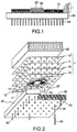
- a first embodiment of an electronic-circuit assembly of the present invention includes a wiring substrate 30 and a plurality of film carriers 1 mounted on the wiring substrate 30.
- Fig. 1 shows four layers of film carriers 1a to 1d, the number of the layers for the film carriers 1 is not limited.
- the film carriers 1a, 1b, 1c and 1d are stacked. Adjacent two of the film carriers 1 in the stack direction are connected to each other in a connection structure described below.
- an LSI chip 20 is mounted. On a circuit surface of the LSI chip 20 is coated with plastic mold resin 22. Between adjacent two of the LSI chips 20 in the stack direction, heating plates, which are not shown, are provided. The heating plates are formed of good thermal conductivity materials such as copper-tungsten alloy.
- On a lower surface of the wiring substrate 30, a plurality of input-output pins 50 are provided.
- each of film carriers 1 includes a flexible film 10.
- the flexible film 10 is made of insulating materials such as polyimide or epoxy resin.
- the flexible film 10 has pliability and has a form of a square having each side of approximately 50 mm.
- the thickness of the flexible film 10 is approximately 50 ⁇ m.
- a device hole for containing the LSI chip 20 is provided in the central portion of the flexible film 10.
- a plurality of through-holes 12 are arranged in a lattice. Each distance in the lattice is approximately 1.27 mm.
- a diameter of each through-hole 12 is approximately 100 ⁇ m.
- lands 13 of conductive materials are provided around the through-hole 12 and on the inner surface thereof. A diameter of each land 13 is approximately 300 ⁇ m.
- a circuit pattern 11 is provided on the flexible film 10.
- a wire width of the circuit pattern 11 is approximately 50 ⁇ m.
- the circuit pattern 11 connects the plurality of through-holes 12 and a plurality of beam leads 14 respectively.
- One ends of the circuit pattern 11 are connected to through-holes 12.
- Another ends of the circuit pattern 11 is connected to one ends of each beam leads 14 on a circumferential edge of the device hole.
- the other ends of the beam leads 14, which is protruding to an inside the device hole, are connected to a pad of the LSI chip 20.
- TAB tape automated bonding
- the wiring substrate 30 is epoxy resin or polyimide reinforced with glass fiber.
- the wiring substrate 30 has a shape of a square having each side of approximately 60 mm.
- the wiring substrate 30 has a thickness of approximately 2.5 mm and high rigidity.
- the wiring substrate 30 is a multi-layer wiring substrate. Ground circuit layers 34 and 36 and power supply source circuit layers 35 and 37 are provided in the inside of the wiring substrate 30.
- a plurality of pads 31 are provided on the upper surface of the wiring substrate 30, a plurality of pads 31 are provided.
- the pads 31 are arranged in positions corresponding to the through-holes 12 of the film carriers 1.
- the pads 31 are arranged in a lattice. Each distance of the lattice is approximately 1.27 mm. Areas, which the pads 31 do not provided, on the upper surface of the wiring substrate 30 are coated with solder resist 32.
- a plurality of input-output pins 50 are provided on the lower surface of the wiring substrate 30, a plurality of input-output pins 50 are provided.
- the input-output pins 50 are arranged in a lattice. Each distance of the lattice is approximately 1.27 mm.
- the input-output pins 50 are connected to the mother board.
- the length of the wiring between the LSI chips and the mother board can be reduced to the minimum by using the input-output pins 50 provided directly under the LSI chips 20 or around them. Since the input-output pins 50 are arranged on the entire lower surface of the wiring substrate 30.
- respective ends of the input-output pins 50 is inserted into respective hole portions 38 on the wiring substrate 30.
- An inserted portion of respective the input-output pins 50 are coated with insulating coating 55.
- the input-output pins 50 are selectively connected to the internal circuit layers of the wiring substrate 30.
- the removed portions of the insulating coating 55 there are provided three types of input-output pins 51 to 53.
- the input-output pin 51 has a removed portion at the top of the insulating coating 55. Therefore, the input-output pin 51 is connected to the power supply source circuit layer 35.
- the input-output pin 52 has a removed portion in the lower part of the insulating coating 55. Therefore, the input-output pin 52 is connected to the power supply source circuit layer 37.
- the input-output pin 53 has a removed portion in the middle part of the insulating coating 55. Therefore, the input-output pin 53 is connected to the ground circuit layer 36. In this manner, the internal circuit layers of the wiring substrate 30 can be selectively connected to the input-output pins 50.
- the wiring substrate 30 has through-holes for signal pins. Pins are inserted into the through-holes for the signal pins without insulating coating.
- a heat sink 60 for heat dissipation is installed on the LSI chip 20 which is mounted on the topmost film carrier 1d.
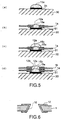
- the through-holes 12a to 12d of the film carriers 1a to 1d are positioned in a straight line on the pad 31 on the wiring substrate 30.
- the through-holes 12a to 12d are connected by solder 15.
- the through-holes 12a to 12d are filled with the solder 15.
- the solder 15 is positioned on the pad 31 of the wiring substrate 30 in a first step. For example, printing is made with creamy solder 15 on the pad 31.
- the stacked film carriers 1a and 1b are positioned on the solder 15 in a second step.
- the solder 15 is heated in a third step.
- the solder 15 melts and a part of it is sucked inside the through-holes 12a and 12b. After that, the solder 15 is cooled down so as to connect the pad 31 with the through-holes 12a and 12b.
- solder 15a is positioned on the pad 31 in a first step.
- a through-hole 12a of a film carrier 1a is connected to the pad 31 in the same manner as for Figs. 4(b) and 4(c) in a second step.
- solder 15b is positioned on the solder 15a in a third step.
- a melting point of the solder 15b is lower than that of the solder 15a.
- a through-hole 12b of a film carrier 1b is connected to the through-hole 12a in the same manner as for Figs. 4(b) and 4(c) in a fourth step.
- a heating temperature of the solder 15b is lower than the melting point of the solder 15a. Therefore, the solder 15a does not melt in the fourth step.
- connection state between the through-holes 12a and 12b can be easily checked. Specifically, it is only required to check that the solder 15 appears inside the topmost through-hole 12b. It can be checked only with viewing the film carrier 1b from the upward position.
- the LSI chip 20 has each side of 20 mm, that the LSI chip 20, the heat conductive plate, and the plastic mold resin have a height of 1 mm in total, that the LSI chips 20 are stacked at 2-mm intervals, that the film carrier 1 has each side of 50 mm, and that four LSI chips 20 are mounted on a single film carrier 1, 16 LSI chips 20 are arranged within a region of a quadrangular prism having each side of 40 mm and a height of 4 mm.
- a circuit region of the LSI chips 20 has a form of a quadrangular prism having each side of 50 mm and a height of 4 mm. Therefore, when the LSI chips 20 are connected to each other by means of three-dimensional orthogonal-system circuit, the wire between the farthest LSI chips 20 has a length of 104 mm or less.
- a mounting area of the LSI chips 20 has a form of a square having each side of 80 mm.
- the wire for connection between the LSI chips 20 spaced farthest to each other has a length of approximately 160 mm. In this manner, the length of the wire between the LSI chips 20 can be reduced according to the present invention.
- the second embodiment is characterized by a structure of through-holes 12. Other structures are essentially the same as for the first embodiment.
- each of the through-holes 12 of the second embodiment has a tapered inner surface.
- the third embodiment of the present invention is characterized by a point that it includes a design change film carrier so as to simplify the design changes. Other structures are essentially the same as for the first embodiment.
- a disconnection means, a connection means, and a switching means are appropriately arranged so as to achieve a desired design change by a combination of these means.
- the disconnection means for a design change film carrier 4a is achieved by means of not providing a through-hole.
- a film carrier 1 has a through-hole 121 at a lattice point 101.
- the design change film carrier 4a does not have any through-hole at the lattice point 101 so as to have an insulation between an upper surface of the design change film carrier 4a and a lower surface thereof.
- a land 41 is arranged instead of a through-hole.
- the land 41 is connected to a through-hole 121 of the film carrier 1 by means of solder. In this manner, a signal through-hole 33 is electrically disconnected from the through-hole 121.
- Materials, a size, and a shape of a flexible film 40 of the design change film carrier 4 may be the same as for the flexible film 10.
- a connection means of a design change film carrier 4b is achieved by a circuit pattern 43 arranged on the design change film carrier 4b.
- the circuit pattern 43 connects a through-hole 421 of the design change film carrier 4b to a through-hole 422 therefor.
- a signal through-hole 331 is connected to a signal through-hole 332.
- a switching means for a design change film carrier 4c is achieved by a combination between the disconnection means and the connection means.
- the film carrier 1 has a through-hole 12 at a lattice point 103.
- the design change film carrier 4c does not have any through-hole at the lattice point 103. Therefore, the through-hole 12 is electrically disconnected from a signal through-hole 331.
- a land 44 is provided instead of a through-hole.
- the land 44 is connected to a through-hole 42 via a circuit pattern 43.
- a through-pole 42 is positioned at a lattice point 104 which is different from the point of the through-hole 12.
- the through-hole 42 is connected to the signal through-hole 332. In this manner, the through-hole 12 which should originally be connected to the signal through-hole 331 can be switched to the signal through-hole 332.
- the design change film carrier 4 can be made in a shorter time in comparison with a multi-layer wiring substrate. Accordingly, a design for an electronic-circuit assembly can be changed in a short time. At present, the design change film carrier 4 can be made in two or three days.
- respective film carriers are connected to each other only by means of soldering between lands arranged around through-holes on upper and lower surfaces of respective film carriers. Accordingly, the design change film carrier 4 can be inserted by melting the solder to separate respective film carriers 12. In addition, the design change film carrier 4 can be made in a short time.
- the design change film carrier 4 is arranged between the wiring substrate 30 and the lowest film carrier 1. It is, however, possible to arrange the design change film carrier 4 in other positions between layers. In addition, it is also possible to use a plurality of design change film carriers 4.
- this embodiment is characterized by a supporting member 61 for supporting the heat sink 60.
- Other structures are essentially the same as for the first embodiment.
- the supporting member 61 has a pillar-shaped foot portion and a plate portion arranged on the foot portion.
- the foot portion of the supporting member 61 is inserted into holes on the flexible film 10 so as to be fixed to the wiring substrate 30.
- the LSI chip 20 of the topmost film carrier 1 is brought into a contact with a lower surface of the plate portion of the supporting member 61.
- the plate portion has holes for containing the topmost through-holes 12. These holes prevent electric contacts between the through-holes 12 and the plate portions.
- the heat sink 60 is installed on the upper surface of the supporting member 61.
- a gap between adjacent flexible films 10 can be filled with resin.
- a gap between the supporting member 61 and the topmost flexible film 10 can be filled with resin. It is preferable that the resin has both of insulation quality and good heat conductivity.
- each LSI chip 20 heat generated from each LSI chip 20 is conducted to the topmost LSI chip 20 via a heat conductive plate arranged between the LSI chips 20.
- the heat conducted to the topmost LSI chip 20 is conducted to the heat sink 60 via a plate portion of the supporting member 61.
- the heat conducted to the heat sink 60 is discharged to the outside air.
- the heat sink 60 is supported by the supporting member 61 and therefore a weight of the heat sink 60 is not weighted to the LSI chips 20. Accordingly, reliability of the LSI chips 20 is not reduced when a large-sized heat sink 60 is used.
- the foot portion of the supporting member 61 serves as a guide of the film carriers 1.
- a plurality of LSI chips 20 can be mounted on a single film carrier 1. Additionally, it is also possible to combine the above-described characteristics of respective embodiments.
- the LSI chips 20 are mounted on the film carriers 1 and a plurality of the film carriers 1 are stacked into a stack in the present invention.
- the film carriers 1 are connected by soldering the through-holes 12 arranged on the film carriers 1.
- a design change can be achieved by putting the design change film carrier 4 between the film carriers 1.
- connection state between the film carriers 1 can be easily checked. Specifically, it is only required to check visually that solder appears inside the topmost through-hole 12.
- a design can be changed in a short time. Specifically, it is only required to insert a design change film carrier 4.
- the design change film carrier 4 can be made in a short time.
- wiring lengths for connection between electronic parts can be reduced. It is because the electronic parts are three-dimensionally mounted.
Landscapes
- Engineering & Computer Science (AREA)
- Microelectronics & Electronic Packaging (AREA)
- Power Engineering (AREA)
- Physics & Mathematics (AREA)
- Condensed Matter Physics & Semiconductors (AREA)
- General Physics & Mathematics (AREA)
- Computer Hardware Design (AREA)
- Manufacturing & Machinery (AREA)
- Combinations Of Printed Boards (AREA)
- Production Of Multi-Layered Print Wiring Board (AREA)
- Cooling Or The Like Of Electrical Apparatus (AREA)
- Structure Of Printed Boards (AREA)
Abstract
Description
- The present invention relates to an electronic-circuit assembly, and more particularly to an electronic asemmbly having a plurality of substrates which are stacked.
- An example of such a conventional electronic-circuit assembly having a laminate made of a plurality of substrates is described in a document disclosed in Rao R. Tummala and Eugene J. Rymaszewski, "Microelectronics Packaging Handbook", 1989, Van Nostrand Reinhold, New York, pp.462-464.
- Referring to Fig. 7-7 of the reference, two ceramic substrates are stacked in this technique. These ceramic substrates are connected to each other by soldering pins protruding from a lower surface of an upper substrate to an upper surface of a lower substrate.
- This prior art, however, has a problem described below.
- First, it is hard to check a connection state between the substrates. It is because the connected portion is covered with the upper substrate.
- Next, it takes a long time for a design change. It is because it requires a longer time to change a design of the ceramic substrates than that of flexible substrates such as tape automated bonding (TAB) tape. Specifically, it takes a few months for a design change of the ceramic substrates, while it takes a few days for a design change of the TAB tape. Particularly, it requires a long time to change it takes a few days for a design change of the TAB tape. Particularly, it requires a long time to change processes of a mask for an internal circuit or a screen therefor.
- In view of the aforementioned problems of the prior art, one object of the present invention is to provide a mounting structure of electronic parts whose connection state between substrates is easily checked.
- Another object of the present invention is to provide a mounting structure of electronic parts whose design can be changed in a short time.
- Yet another object of the present invention is to provide a method of reducing a length of connection wire between electronic parts.
- According to the present invention, an electronic-circuit assembly comprises a plurality of stacked substrates having through-holes respectively and a connection member having electric conductivity and connecting adjacent through-holes of said substrates to each other in the stack direction of said substrates.
- In another aspect of the present invention, the electronic-circuit assembly may further comprising a wiring substrate, said wiring substrate including a first surface on which said plurality of substrates are mounted, and terminals provided on said first surface and connected to said through-holes in the lowest one of said plurality of substrates by said connection member.
- In yet another aspect of the present invention, the electronic-circuit assembly, wherein said plurality of substrates includes conductive pads which are provided on upper and lower surfaces of said substrates, surround said through-holes, and are connected to said through-holes of said substrate and wherein connections between said plurality of substrates are made by connecting said conductive pads to each other by said connection member in said plurality of substrates.
- Other features and advantages of the invention will be made more apparent by the detailed description hereunder taken in conjunction with the accompanying drawings, wherein:
- Fig. 1 is a drawing illustrating a structure of a first embodiment of the present invention;
- Fig. 2 is an exploded view illustrating a structure of the first embodiment of the present invention;
- Fig. 3 is a drawing illustrating a detailed structure of the first embodiment of the present invention;
- Fig. 4 is a drawing illustrating a manufacturing method of the first embodiment of the present invention;
- Fig. 5 is a drawing illustrating another manufacturing method of the first embodiment of the present invention;
- Fig. 6 is a drawing illustrating a structure of a through-
hole 12 of a second embodiment of the present invention; - Fig. 7 is a drawing illustrating a structure of a design change film carrier 4 of a third embodiment of the present invention; and
- Fig. 8 is a drawing illustrating a structure of a fourth embodiment of the present invention.
- In the drawings, the same reference numerals represent the same structural elements.
- This invention will be described below by using the accompanying drawings.
- Referring to Fig. 1, a first embodiment of an electronic-circuit assembly of the present invention includes a
wiring substrate 30 and a plurality offilm carriers 1 mounted on thewiring substrate 30. Although Fig. 1 shows four layers offilm carriers 1a to 1d, the number of the layers for thefilm carriers 1 is not limited. Thefilm carriers film carriers 1 in the stack direction are connected to each other in a connection structure described below. At the center of each offilm carriers 1, anLSI chip 20 is mounted. On a circuit surface of theLSI chip 20 is coated withplastic mold resin 22. Between adjacent two of theLSI chips 20 in the stack direction, heating plates, which are not shown, are provided. The heating plates are formed of good thermal conductivity materials such as copper-tungsten alloy. On a lower surface of thewiring substrate 30, a plurality of input-output pins 50 are provided. - Referring to Figs. 2 and 3, each of
film carriers 1 includes aflexible film 10. Theflexible film 10 is made of insulating materials such as polyimide or epoxy resin. Theflexible film 10 has pliability and has a form of a square having each side of approximately 50 mm. The thickness of theflexible film 10 is approximately 50 µm. - In the central portion of the
flexible film 10, a device hole for containing theLSI chip 20 is provided. In the outside of the device hole, a plurality of through-holes 12 are arranged in a lattice. Each distance in the lattice is approximately 1.27 mm. A diameter of each through-hole 12 is approximately 100 µm. Around the through-hole 12 and on the inner surface thereof,lands 13 of conductive materials are provided. A diameter of eachland 13 is approximately 300 µm. - On the
flexible film 10, acircuit pattern 11 is provided. A wire width of thecircuit pattern 11 is approximately 50 µm. Thecircuit pattern 11 connects the plurality of through-holes 12 and a plurality of beam leads 14 respectively. One ends of thecircuit pattern 11 are connected to through-holes 12. Another ends of thecircuit pattern 11 is connected to one ends of each beam leads 14 on a circumferential edge of the device hole. The other ends of the beam leads 14, which is protruding to an inside the device hole, are connected to a pad of theLSI chip 20. - For manufacturing the
film carriers 1 and mounting theLSI chips 20, a tape automated bonding (TAB) technique can be used. Details of the TAB techniques are described in, for example, in a document written by Rao R. Tummala and Eugene J. Rymaszewski "Microelectronics Packaging Handbook" 1989, Van Nostrand Reinhold, New York, pp. 409 to pp. 454. Afilm carrier 1 produced by using the TAB technique is called a TAB tape carrier. - Materials of the
wiring substrate 30 are epoxy resin or polyimide reinforced with glass fiber. Thewiring substrate 30 has a shape of a square having each side of approximately 60 mm. Thewiring substrate 30 has a thickness of approximately 2.5 mm and high rigidity. Thewiring substrate 30 is a multi-layer wiring substrate. Ground circuit layers 34 and 36 and power supply source circuit layers 35 and 37 are provided in the inside of thewiring substrate 30. - On the upper surface of the
wiring substrate 30, a plurality ofpads 31 are provided. Thepads 31 are arranged in positions corresponding to the through-holes 12 of thefilm carriers 1. In other words, thepads 31 are arranged in a lattice. Each distance of the lattice is approximately 1.27 mm. Areas, which thepads 31 do not provided, on the upper surface of thewiring substrate 30 are coated with solder resist 32. - On the lower surface of the
wiring substrate 30, a plurality of input-output pins 50 are provided. The input-output pins 50 are arranged in a lattice. Each distance of the lattice is approximately 1.27 mm. When the electronic-circuit assembly is mounted on a mother board, the input-output pins 50 are connected to the mother board. The length of the wiring between the LSI chips and the mother board can be reduced to the minimum by using the input-output pins 50 provided directly under the LSI chips 20 or around them. Since the input-output pins 50 are arranged on the entire lower surface of thewiring substrate 30. - Referring to Fig. 3, respective ends of the input-
output pins 50 is inserted intorespective hole portions 38 on thewiring substrate 30. An inserted portion of respective the input-output pins 50 are coated with insulatingcoating 55. With removing a part of the insulatingcoating 55 to expose conductive portions, the input-output pins 50 are selectively connected to the internal circuit layers of thewiring substrate 30. According to the removed portions of the insulatingcoating 55, there are provided three types of input-output pins 51 to 53. The input-output pin 51 has a removed portion at the top of the insulatingcoating 55. Therefore, the input-output pin 51 is connected to the power supplysource circuit layer 35. The input-output pin 52 has a removed portion in the lower part of the insulatingcoating 55. Therefore, the input-output pin 52 is connected to the power supplysource circuit layer 37. The input-output pin 53 has a removed portion in the middle part of the insulatingcoating 55. Therefore, the input-output pin 53 is connected to theground circuit layer 36. In this manner, the internal circuit layers of thewiring substrate 30 can be selectively connected to the input-output pins 50. In addition, thewiring substrate 30 has through-holes for signal pins. Pins are inserted into the through-holes for the signal pins without insulating coating. - Referring to Figs. 2 and 3, a
heat sink 60 for heat dissipation is installed on theLSI chip 20 which is mounted on thetopmost film carrier 1d. - Next, a connection structure between the
film carriers 1a to 1d is described below. - Referring to Fig. 3, the through-
holes 12a to 12d of thefilm carriers 1a to 1d are positioned in a straight line on thepad 31 on thewiring substrate 30. The through-holes 12a to 12d are connected bysolder 15. The through-holes 12a to 12d are filled with thesolder 15. - Then, a manufacturing method of the mounting structure of this embodiment is described below by using the accompanying drawing. Specifically, a description will be made on a method of stacking the
film carriers wiring substrate 30. In this stacking method, a plurality offilm carriers 1 are connected at a time. - Referring to Fig. 4(a), the
solder 15 is positioned on thepad 31 of thewiring substrate 30 in a first step. For example, printing is made withcreamy solder 15 on thepad 31. - Referring to Fig. 4(b), the stacked
film carriers solder 15 in a second step. - Referring to Fig. 4(c), the
solder 15 is heated in a third step. Thesolder 15 melts and a part of it is sucked inside the through-holes solder 15 is cooled down so as to connect thepad 31 with the through-holes - Subsequently, another stacking method is described below. In this stacking method, the
film carriers 1 are stacked sequentially. - Referring to Fig. 5(a),
solder 15a is positioned on thepad 31 in a first step. - Referring to Fig. 5(b), a through-
hole 12a of afilm carrier 1a is connected to thepad 31 in the same manner as for Figs. 4(b) and 4(c) in a second step. - Referring to Fig. 5(c),
solder 15b is positioned on thesolder 15a in a third step. A melting point of thesolder 15b is lower than that of thesolder 15a. - Referring to Fig. 5(d), a through-
hole 12b of afilm carrier 1b is connected to the through-hole 12a in the same manner as for Figs. 4(b) and 4(c) in a fourth step. A heating temperature of thesolder 15b is lower than the melting point of thesolder 15a. Therefore, thesolder 15a does not melt in the fourth step. - In the above manufacturing method, the connection state between the through-
holes solder 15 appears inside the topmost through-hole 12b. It can be checked only with viewing thefilm carrier 1b from the upward position. - In the first embodiment, assuming that the
LSI chip 20 has each side of 20 mm, that theLSI chip 20, the heat conductive plate, and the plastic mold resin have a height of 1 mm in total, that the LSI chips 20 are stacked at 2-mm intervals, that thefilm carrier 1 has each side of 50 mm, and that fourLSI chips 20 are mounted on asingle film carrier LSI chips 20 are arranged within a region of a quadrangular prism having each side of 40 mm and a height of 4 mm. A circuit region of the LSI chips 20 has a form of a quadrangular prism having each side of 50 mm and a height of 4 mm. Therefore, when the LSI chips 20 are connected to each other by means of three-dimensional orthogonal-system circuit, the wire between the farthest LSI chips 20 has a length of 104 mm or less. - On the other hand, if the above-described 16
LSI chips 20 are mounted on a substrate of a single layer, a mounting area of the LSI chips 20 has a form of a square having each side of 80 mm. In this structure, the wire for connection between the LSI chips 20 spaced farthest to each other has a length of approximately 160 mm. In this manner, the length of the wire between the LSI chips 20 can be reduced according to the present invention. - Next, a second embodiment of the present invention is described below by using the accompanying drawings. The second embodiment is characterized by a structure of through-
holes 12. Other structures are essentially the same as for the first embodiment. - Referring to Fig. 6, each of the through-
holes 12 of the second embodiment has a tapered inner surface. - Next, a third embodiment of the present invention is described below by using the accompanying drawings. The third embodiment of the present invention is characterized by a point that it includes a design change film carrier so as to simplify the design changes. Other structures are essentially the same as for the first embodiment. On the design change film carrier, a disconnection means, a connection means, and a switching means are appropriately arranged so as to achieve a desired design change by a combination of these means.
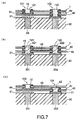
- Referring to Fig. 7(a), the disconnection means for a design
change film carrier 4a is achieved by means of not providing a through-hole. Afilm carrier 1 has a through-hole 121 at alattice point 101. On the other hand, the designchange film carrier 4a does not have any through-hole at thelattice point 101 so as to have an insulation between an upper surface of the designchange film carrier 4a and a lower surface thereof. At thelattice point 101 on the upper surface of the designchange film carrier 4a, a land 41 is arranged instead of a through-hole. The land 41 is connected to a through-hole 121 of thefilm carrier 1 by means of solder. In this manner, a signal through-hole 33 is electrically disconnected from the through-hole 121. Materials, a size, and a shape of aflexible film 40 of the design change film carrier 4 may be the same as for theflexible film 10. - Referring to Fig. 7(b), a connection means of a design
change film carrier 4b is achieved by acircuit pattern 43 arranged on the designchange film carrier 4b. Thecircuit pattern 43 connects a through-hole 421 of the designchange film carrier 4b to a through-hole 422 therefor. By this connection, a signal through-hole 331 is connected to a signal through-hole 332. - Referring to Figs. 7(c), a switching means for a design
change film carrier 4c is achieved by a combination between the disconnection means and the connection means. Thefilm carrier 1 has a through-hole 12 at alattice point 103. The designchange film carrier 4c does not have any through-hole at thelattice point 103. Therefore, the through-hole 12 is electrically disconnected from a signal through-hole 331. At thelattice point 103 on an upper surface of the designchange film carrier 4c, aland 44 is provided instead of a through-hole. Theland 44 is connected to a through-hole 42 via acircuit pattern 43. A through-pole 42 is positioned at alattice point 104 which is different from the point of the through-hole 12. The through-hole 42 is connected to the signal through-hole 332. In this manner, the through-hole 12 which should originally be connected to the signal through-hole 331 can be switched to the signal through-hole 332. - With combinations of the switching means, the connection means, and the disconnection means, various design changes are achieved. The design change film carrier 4 can be made in a shorter time in comparison with a multi-layer wiring substrate. Accordingly, a design for an electronic-circuit assembly can be changed in a short time. At present, the design change film carrier 4 can be made in two or three days.
- According to this embodiment, respective film carriers are connected to each other only by means of soldering between lands arranged around through-holes on upper and lower surfaces of respective film carriers. Accordingly, the design change film carrier 4 can be inserted by melting the solder to separate
respective film carriers 12. In addition, the design change film carrier 4 can be made in a short time. - In this embodiment, the design change film carrier 4 is arranged between the
wiring substrate 30 and thelowest film carrier 1. It is, however, possible to arrange the design change film carrier 4 in other positions between layers. In addition, it is also possible to use a plurality of design change film carriers 4. - Next, a fourth embodiment of the present invention is described below by using the drawings.
- Referring to Fig. 8, this embodiment is characterized by a supporting
member 61 for supporting theheat sink 60. Other structures are essentially the same as for the first embodiment. - The supporting
member 61 has a pillar-shaped foot portion and a plate portion arranged on the foot portion. The foot portion of the supportingmember 61 is inserted into holes on theflexible film 10 so as to be fixed to thewiring substrate 30. At this point, theLSI chip 20 of thetopmost film carrier 1 is brought into a contact with a lower surface of the plate portion of the supportingmember 61. The plate portion has holes for containing the topmost through-holes 12. These holes prevent electric contacts between the through-holes 12 and the plate portions. Theheat sink 60 is installed on the upper surface of the supportingmember 61. - A gap between adjacent
flexible films 10 can be filled with resin. In addition, a gap between the supportingmember 61 and the topmostflexible film 10 can be filled with resin. It is preferable that the resin has both of insulation quality and good heat conductivity. - In this structure, heat generated from each
LSI chip 20 is conducted to thetopmost LSI chip 20 via a heat conductive plate arranged between the LSI chips 20. The heat conducted to thetopmost LSI chip 20 is conducted to theheat sink 60 via a plate portion of the supportingmember 61. The heat conducted to theheat sink 60 is discharged to the outside air. - In the fourth embodiment, the
heat sink 60 is supported by the supportingmember 61 and therefore a weight of theheat sink 60 is not weighted to the LSI chips 20. Accordingly, reliability of the LSI chips 20 is not reduced when a large-sized heat sink 60 is used. In addition, the foot portion of the supportingmember 61 serves as a guide of thefilm carriers 1. - Subsequently, another embodiment of the present invention is described below.
- A plurality of
LSI chips 20 can be mounted on asingle film carrier 1. Additionally, it is also possible to combine the above-described characteristics of respective embodiments. - As described above, the LSI chips 20 are mounted on the
film carriers 1 and a plurality of thefilm carriers 1 are stacked into a stack in the present invention. Thefilm carriers 1 are connected by soldering the through-holes 12 arranged on thefilm carriers 1. A design change can be achieved by putting the design change film carrier 4 between thefilm carriers 1. This electronic-circuit assembly has the following effects. - First, a connection state between the
film carriers 1 can be easily checked. Specifically, it is only required to check visually that solder appears inside the topmost through-hole 12. - Second, a design can be changed in a short time. Specifically, it is only required to insert a design change film carrier 4. The design change film carrier 4 can be made in a short time.
- Third, wiring lengths for connection between electronic parts can be reduced. It is because the electronic parts are three-dimensionally mounted.
- While this invention has been described in conjunction with the preferred embodiments thereof, it will now readily be possible for those skilled in the art to put this invention into practice in various other manners.
Claims (18)
- An electronic-circuit assembly comprising:a plurality of stacked substrates having through-holes respectively; anda connection member having electric conductivity and connecting adjacent through-holes of said substrates to each other in the stack direction of said substrates.
- The electronic-circuit assembly as claimed in claim 1, further comprising a wiring substrate,
said wiring substrate including:a first surface on which said plurality of substrates are mounted, and;terminals provided on said first surface and connected to said through-holes in the lowest one of said plurality of substrates by said connection member. - The electronic-circuit assembly as claimed in claim 1, wherein said plurality of substrates includes conductive pads which are provided on upper and lower surfaces of said substrates, surround said through-holes, and are connected to said through-holes of said substrate; and
wherein connections between said plurality of substrates are made by connecting said conductive pads to each other by said connection member in said plurality of substrates. - The electronic-circuit assembly as claimed in claim 1,
further comprising an integrated circuit chip mounted on at least one of said plurality of substrates. - The electronic-circuit assembly as claimed in claim 1,
wherein said through-holes are arranged in a lattice in each of said plurality of substrates. - The electronic-circuit assembly as claimed in claim 1,
wherein at least one of said plurality of substrates is an insulating substrate which has no through-holes at the positions corresponding to said through-holes. - The electronic-circuit assembly as claimed in claim 1,
wherein at least one of said plurality of substrates is a connection substrate having a first through-hole, a second through-hole, and a circuit connecting between said first through-hole and said second through-hole. - The electronic-circuit assembly as claimed in claim 1,
wherein said plurality of substrates comprises:a first substrate having a first through-hole and a connection member provided in the first through-hole; anda second substrate having a terminal provided at a position corresponding to said first through-hole of said first substrate and connected to said connection member provided in the first through-hole, a circuit connected to said terminal, and a second through-hole connected to said circuit. - The electronic-circuit assembly as claimed in claim 1, further comprising:an integrated circuit chip mounted at least on the topmost substrate out of said plurality of substrates;a heat dissipation member thermally connected to said integrated circuit chip; anda supporting means for supporting said heat dissipation member on said wiring substrate.
- The electronic-circuit assembly as claimed in claim 1, wherein said through-holes have a tapered inner surface.
- The electronic-circuit assembly as claimed in claim 1,
wherein each of said plurality of substrates has flexibility. - The electronic-circuit assembly as claimed in claim 1, wherein said connection member is solder.
- An electronic-circuit assembly comprising:a first substrate having first through-holes;a second substrate laid on the first substrate, having second through-holes opposing to said first through-holes; anda connection member for connecting said first through-holes to said second through-holes.
- The electronic-circuit assembly as claimed in claim 1,
wherein each of said first and second substrates has flexibility and said first substrate is arranged under said second substrate; and
further comprising a first plane on which said first substrate is mounted and a wiring substrate having terminals connected to said first through-holes of said first substrate by means of said connection member. - A method of manufacturing an electronic-circuit assembly including a first substrate having first through-holes and a second substrate having second through-holes, comprising:a step of applying solder into said first through-holes;a step of positioning said second flexible substrate so that said second through-holes oppose to said solder; anda step of melting said solder, moving at least a part of said solder into said second through-holes, and connecting said first and second through-holes to each other by means of said solder.
- A method of manufacturing an electronic-circuit assembly including a wiring substrate having terminals, a first substrate having first through-holes, and a second substrate having second through-holes, comprising:a step of applying solder on said terminals of said wiring substrate;a step of positioning said first substrate so that said first through-holes opposite to said solder and positioning said second substrate so that said second through-holes opposite to said first through-holes; anda step of melting said solder, moving at least a part of said solder into said first and second through-holes, and connecting said terminals of said wiring substrate, said first through-holes of said first substrate, and said second through-holes of said second substrate by means of said solder.
- A method of manufacturing electronic-circuit assembly including a wiring substrate having terminals, a first substrate having first through-holes, and a second substrate having second through-holes, comprising:a step of applying first solder on said terminals of said wiring substrate;a step of positioning said first substrate so that said first through-holes opposite to said solder;a step of melting said solder, moving at least a part of said first solder into said first through-holes, and connecting said terminals of said wiring substrate and said first through-holes of said first substrate by means of said first solder;a step of applying second solder whose melting point is lower than that of said first solder on said first through-hole;a step of positioning said second substrate so that said second through-holes opposite to said second solder; anda step of melting said second solder at a temperature lower than the melting point of said first solder, moving at least a part of said second solder into said second through-holes, and connecting said first and second through-holes by means of said second solder.
- A method of manufacturing an electronic-circuit assembly for connecting a plurality of stacked substrates each having through-holes, comprising:a step of connecting two adjacent of said through-holes to each other in the stack direction of said substrates out of said through-holes of said plurality of substrates; anda step of checking a connection state between said through-holes by viewing that said solder appears inside said through-holes of the topmost substrate out of said plurality of substrates.
Applications Claiming Priority (2)
| Application Number | Priority Date | Filing Date | Title |
|---|---|---|---|
| JP8055683A JP2820108B2 (en) | 1996-03-13 | 1996-03-13 | Electronic component mounting structure and method of manufacturing the same |
| JP55683/96 | 1996-03-13 |
Publications (2)
| Publication Number | Publication Date |
|---|---|
| EP0795906A2 true EP0795906A2 (en) | 1997-09-17 |
| EP0795906A3 EP0795906A3 (en) | 1998-07-22 |
Family
ID=13005709
Family Applications (1)
| Application Number | Title | Priority Date | Filing Date |
|---|---|---|---|
| EP97104269A Withdrawn EP0795906A3 (en) | 1996-03-13 | 1997-03-13 | An electronic-circuit assembly and its manufacturing method |
Country Status (4)
| Country | Link |
|---|---|
| US (1) | US5892657A (en) |
| EP (1) | EP0795906A3 (en) |
| JP (1) | JP2820108B2 (en) |
| CA (1) | CA2199796C (en) |
Cited By (2)
| Publication number | Priority date | Publication date | Assignee | Title |
|---|---|---|---|---|
| EP0942636A2 (en) * | 1998-03-12 | 1999-09-15 | Lucent Technologies Inc. | Solder bonding printed circuit board |
| WO2001015508A2 (en) * | 1999-08-20 | 2001-03-01 | Cardiac Pacemakers, Inc. | Integrated emi shield utilizing a hybrid edge |
Families Citing this family (16)
| Publication number | Priority date | Publication date | Assignee | Title |
|---|---|---|---|---|
| US6734545B1 (en) * | 1995-11-29 | 2004-05-11 | Hitachi, Ltd. | BGA type semiconductor device and electronic equipment using the same |
| US6462950B1 (en) * | 2000-11-29 | 2002-10-08 | Nokia Mobile Phones Ltd. | Stacked power amplifier module |
| DE10152475A1 (en) * | 2001-10-24 | 2003-05-08 | Hella Kg Hueck & Co | Heat conducting connecting piece has protrusions on surfaces of parts butting onto insulating film corresponding to apertures of other part |
| JP3826875B2 (en) | 2002-10-29 | 2006-09-27 | セイコーエプソン株式会社 | Piezoelectric device and manufacturing method thereof |
| US6657864B1 (en) * | 2002-12-16 | 2003-12-02 | International Business Machines Corporation | High density thermal solution for direct attach modules |
| WO2004112450A1 (en) * | 2003-06-12 | 2004-12-23 | Fujitsu Limited | Board mounting method and mounting structure |
| US6974333B2 (en) * | 2004-03-30 | 2005-12-13 | General Electric Company | High-density connection between multiple circuit boards |
| JP2007273654A (en) * | 2006-03-31 | 2007-10-18 | Sumitomo Bakelite Co Ltd | Flexible circuit board, method for manufacturing the same, and electronic component |
| US7926173B2 (en) * | 2007-07-05 | 2011-04-19 | Occam Portfolio Llc | Method of making a circuit assembly |
| KR101489034B1 (en) * | 2008-12-19 | 2015-02-04 | 후루카와 덴키 고교 가부시키가이샤 | Multilayer printed board and method for manufacturing the same |
| JP5741105B2 (en) * | 2011-03-22 | 2015-07-01 | セイコーエプソン株式会社 | Electro-optic device |
| KR102223784B1 (en) * | 2014-06-03 | 2021-03-08 | 삼성디스플레이 주식회사 | Flexible circuit film and display apparatus having the same |
| DE102014013565A1 (en) * | 2014-09-18 | 2016-03-24 | Plastic Electronic Gmbh | Circuit carrier foil PCB assembly |
| WO2018220717A1 (en) * | 2017-05-30 | 2018-12-06 | 新電元工業株式会社 | Electronic device and method for manufacturing same |
| US11257742B2 (en) * | 2020-07-02 | 2022-02-22 | Advanced Semiconductor Engineering, Inc. | Wiring structure and method for manufacturing the same |
| US11355426B2 (en) * | 2020-07-31 | 2022-06-07 | Advanced Semiconductor Engineering, Inc. | Wiring structure and method for manufacturing the same |
Citations (5)
| Publication number | Priority date | Publication date | Assignee | Title |
|---|---|---|---|---|
| US5128831A (en) * | 1991-10-31 | 1992-07-07 | Micron Technology, Inc. | High-density electronic package comprising stacked sub-modules which are electrically interconnected by solder-filled vias |
| WO1993013637A1 (en) * | 1991-12-31 | 1993-07-08 | Tessera, Inc. | Multi-layer circuit construction methods and structures with customization features and components for use therein |
| EP0561620A2 (en) * | 1992-03-19 | 1993-09-22 | Hitachi, Ltd. | Wiring sheet assemblies, and forming electrical connections thereof |
| US5384955A (en) * | 1992-09-29 | 1995-01-31 | International Business Machines Corporation | Method for replacing IC chip package interposer |
| FR2724052A1 (en) * | 1994-08-31 | 1996-03-01 | Nec Corp | Assembly method for large scale integrated circuits |
Family Cites Families (3)
| Publication number | Priority date | Publication date | Assignee | Title |
|---|---|---|---|---|
| JPS6447081U (en) * | 1987-09-16 | 1989-03-23 | ||
| JP2758099B2 (en) * | 1992-02-27 | 1998-05-25 | シャープ株式会社 | Multi-layer flexible printed wiring board |
| JPH0766557A (en) * | 1993-08-31 | 1995-03-10 | Mitsubishi Gas Chem Co Inc | Manufacture of rigid and flexible multilayer printed board |
-
1996
- 1996-03-13 JP JP8055683A patent/JP2820108B2/en not_active Expired - Fee Related
-
1997
- 1997-03-12 CA CA002199796A patent/CA2199796C/en not_active Expired - Fee Related
- 1997-03-13 US US08/816,671 patent/US5892657A/en not_active Expired - Fee Related
- 1997-03-13 EP EP97104269A patent/EP0795906A3/en not_active Withdrawn
Patent Citations (5)
| Publication number | Priority date | Publication date | Assignee | Title |
|---|---|---|---|---|
| US5128831A (en) * | 1991-10-31 | 1992-07-07 | Micron Technology, Inc. | High-density electronic package comprising stacked sub-modules which are electrically interconnected by solder-filled vias |
| WO1993013637A1 (en) * | 1991-12-31 | 1993-07-08 | Tessera, Inc. | Multi-layer circuit construction methods and structures with customization features and components for use therein |
| EP0561620A2 (en) * | 1992-03-19 | 1993-09-22 | Hitachi, Ltd. | Wiring sheet assemblies, and forming electrical connections thereof |
| US5384955A (en) * | 1992-09-29 | 1995-01-31 | International Business Machines Corporation | Method for replacing IC chip package interposer |
| FR2724052A1 (en) * | 1994-08-31 | 1996-03-01 | Nec Corp | Assembly method for large scale integrated circuits |
Non-Patent Citations (1)
| Title |
|---|
| DOHYA AKIHIRO ET AL: "PACKAGING TECHNOLOGY FOR THE NEC SX-3/SX-X SUPERCOMPUTER" PROCEEDINGS OF THE ELECTRONIC COMPONENTS AND TECHNOLOGY CONFERENCE, LAS VEGAS, MAY 20 - 23, 1990, vol. VOL. 1, no. CONF. 40, 20 May 1990, INSTITUTE OF ELECTRICAL AND ELECTRONICS ENGINEERS, pages 525-533, XP000144725 * |
Cited By (5)
| Publication number | Priority date | Publication date | Assignee | Title |
|---|---|---|---|---|
| EP0942636A2 (en) * | 1998-03-12 | 1999-09-15 | Lucent Technologies Inc. | Solder bonding printed circuit board |
| EP0942636A3 (en) * | 1998-03-12 | 2001-03-14 | Lucent Technologies Inc. | Solder bonding printed circuit board |
| WO2001015508A2 (en) * | 1999-08-20 | 2001-03-01 | Cardiac Pacemakers, Inc. | Integrated emi shield utilizing a hybrid edge |
| WO2001015508A3 (en) * | 1999-08-20 | 2001-09-27 | Cardiac Pacemakers Inc | Integrated emi shield utilizing a hybrid edge |
| US6865804B2 (en) | 1999-08-20 | 2005-03-15 | Cardiac Pacemakers, Inc. | Method for integrated EMI shielding |
Also Published As
| Publication number | Publication date |
|---|---|
| CA2199796C (en) | 2002-01-22 |
| CA2199796A1 (en) | 1997-09-13 |
| US5892657A (en) | 1999-04-06 |
| JP2820108B2 (en) | 1998-11-05 |
| EP0795906A3 (en) | 1998-07-22 |
| JPH09246683A (en) | 1997-09-19 |
Similar Documents
| Publication | Publication Date | Title |
|---|---|---|
| CA2199796C (en) | An electronic-circuit assembly and its manufacturing method | |
| JP2996510B2 (en) | Electronic circuit board | |
| US4385202A (en) | Electronic circuit interconnection system | |
| US7183658B2 (en) | Low cost microelectronic circuit package | |
| EP0575806B1 (en) | Package for integrated circuit chips | |
| US5637832A (en) | Solder ball array and method of preparation | |
| US5039628A (en) | Flip substrate for chip mount | |
| US4926241A (en) | Flip substrate for chip mount | |
| US6504104B2 (en) | Flexible wiring for the transformation of a substrate with edge contacts into a ball grid array | |
| JP3898891B2 (en) | Via plug adapter | |
| US5412539A (en) | Multichip module with a mandrel-produced interconnecting decal | |
| EP0622847A2 (en) | Three dimensional package and architecture for high performance computer | |
| US4472762A (en) | Electronic circuit interconnection system | |
| US5760469A (en) | Semiconductor device and semiconductor device mounting board | |
| EP0073149A2 (en) | Semiconductor chip mounting module | |
| EP0279996A1 (en) | Multiple chip interconnection system and package | |
| US20020134582A1 (en) | Integrated circuit package and method | |
| JPH06103704B2 (en) | Method of manufacturing integrated circuit package, integrated circuit assembly and method of forming vias | |
| JP3483280B2 (en) | Three-dimensional interconnection method of electronic component package and three-dimensional component formed thereby | |
| JP3247634B2 (en) | Semiconductor device package and assembling method | |
| US4546406A (en) | Electronic circuit interconnection system | |
| US4731700A (en) | Semiconductor connection and crossover apparatus | |
| JPH0529537A (en) | Semiconductor module structure | |
| EP0521720A1 (en) | Heat-dissipating multi-layer circuit board | |
| JPH09326450A (en) | Semiconductor device and its manufacture |
Legal Events
| Date | Code | Title | Description |
|---|---|---|---|
| PUAI | Public reference made under article 153(3) epc to a published international application that has entered the european phase |
Free format text: ORIGINAL CODE: 0009012 |
|
| AK | Designated contracting states |
Kind code of ref document: A2 Designated state(s): DE FR GB |
|
| PUAL | Search report despatched |
Free format text: ORIGINAL CODE: 0009013 |
|
| AK | Designated contracting states |
Kind code of ref document: A3 Designated state(s): DE FR GB |
|
| 17P | Request for examination filed |
Effective date: 19981105 |
|
| 17Q | First examination report despatched |
Effective date: 20040706 |
|
| STAA | Information on the status of an ep patent application or granted ep patent |
Free format text: STATUS: THE APPLICATION IS DEEMED TO BE WITHDRAWN |
|
| 18D | Application deemed to be withdrawn |
Effective date: 20041117 |