EP0792073A2 - Color signal adjustment apparatus - Google Patents
Color signal adjustment apparatus Download PDFInfo
- Publication number
- EP0792073A2 EP0792073A2 EP97301004A EP97301004A EP0792073A2 EP 0792073 A2 EP0792073 A2 EP 0792073A2 EP 97301004 A EP97301004 A EP 97301004A EP 97301004 A EP97301004 A EP 97301004A EP 0792073 A2 EP0792073 A2 EP 0792073A2
- Authority
- EP
- European Patent Office
- Prior art keywords
- signal
- gain
- phase
- quadrant
- signals
- Prior art date
- Legal status (The legal status is an assumption and is not a legal conclusion. Google has not performed a legal analysis and makes no representation as to the accuracy of the status listed.)
- Granted
Links
Images


Classifications
-
- H—ELECTRICITY
- H04—ELECTRIC COMMUNICATION TECHNIQUE
- H04N—PICTORIAL COMMUNICATION, e.g. TELEVISION
- H04N9/00—Details of colour television systems
- H04N9/64—Circuits for processing colour signals
-
- H—ELECTRICITY
- H04—ELECTRIC COMMUNICATION TECHNIQUE
- H04N—PICTORIAL COMMUNICATION, e.g. TELEVISION
- H04N9/00—Details of colour television systems
- H04N9/64—Circuits for processing colour signals
- H04N9/68—Circuits for processing colour signals for controlling the amplitude of colour signals, e.g. automatic chroma control circuits
-
- H—ELECTRICITY
- H04—ELECTRIC COMMUNICATION TECHNIQUE
- H04N—PICTORIAL COMMUNICATION, e.g. TELEVISION
- H04N9/00—Details of colour television systems
- H04N9/64—Circuits for processing colour signals
- H04N9/67—Circuits for processing colour signals for matrixing
Landscapes
- Engineering & Computer Science (AREA)
- Multimedia (AREA)
- Signal Processing (AREA)
- Processing Of Color Television Signals (AREA)
Abstract
Description
- This invention relates to color signal adjustment apparatus which can be used in, for example, a camera device.
- There is known a camera device in which red (R), green (G) and blue (B) color signals, obtained on imaging an object, are processed with chroma signal processing for generating (R-Y) and (B-Y) color difference signals. In this camera device, the (R-Y) and (B-Y) signals are found by the following equations:

- X: gain of the (R-Y) signal and
- Z: phase of the (R-Y) signal
- X: gain of the (B-Y) signal
- Z: phase of the (B-Y) signal.
- Therefore, in adjusting the color signal using these color signals, the signs of the (R-G) signal and the (B-G) signal as parameters are discriminated for deciding whether these signals define the (R-Y) signal or the (B-G) signal. Subsequently, the coefficients of X and G are determined. That is, if the sign of the (R-G) signal is plus or minus, the gain of the (R-Y) signal becomes positive or negative, respectively. On the other hand, if the sign of the (B-G) signal is plus or minus, the phase of the (R-Y) signal becomes positive or negative, respectively.
- Similarly, if the sign of the (R-G) signal is plus or minus, the phase of the (B-Y) signal becomes positive or negative, respectively. On the other hand, if the sign of the (B-G) signal is plus or minus, the gain of the (B-Y) signal becomes positive or negative, respectively.
- After the signs of the gain and the phase are set in this manner, X and Z are set.
- However, since the (R-Y) and(B-Y) signals have the (R-G) and (B-G) signals as parameters, respectively, as described above, the phase of the (B-Y) signal is increased if the gain of the (R-Y) signal is increased, such that the phase or the gain, which are not desired to be adjusted, are undesirably changed.
- On the other hand, there are eight parameters of the (R-Y) and (B-Y) signals in all, as described above, such that, if each parameter is of one bit, eight bits are perpetually required. The result is that, if color signal adjustment employing the above-mentioned eight color difference signals for each pixel, the information volume becomes excessive, thus delaying the transfer rate of each parameter.
- It is therefore an aim of the present invention to provide a color signal adjustment circuit in which specified color signals can be adjusted and in which color signal adjustment can be realized with a small information volume.
- The color signal adjustment apparatus according to the present invention includes first color difference signal generating means for generating a (R-G) signal and a (B-G) signal from R, G and B signals, and second color difference generating means for generating, in a (B-Y) - (B-G) coordinate system having a (B-Y) signal and an (R-Y) signal as an abscissa and an ordinate, respectively, the (R-Y) signal and the (B-Y) signal, using the (R-G) signal and the (B-G) signal from the first color difference signal generating means, in accordance with the following equations:

- X: gain of the (R-Y) signal
- Z: phase of the (R-Y) signal; and
- X: gain of the (B-Y) signal; and
- Z: phase of the (B-Y) signal.
- The color signal adjustment apparatus according to the present invention also includes first parameter outputting means for outputting a gain and a phase for the (R-Y) signal and a gain and a phase for the (B-Y) signal in the first quadrant in the (B-Y) - (R-Y) coordinate system, and second parameter outputting means for outputting a gain and a phase for the (R-Y) signal and a gain and a phase for the (B-Y) signal in the second quadrant in the (B-Y) - (R-Y) coordinate system. The color signal adjustment apparatus also includes third parameter outputting means for outputting a gain and a phase for the (R-Y) signal and a gain and a phase for the (B-Y) signal in the third quadrant in the (B-Y) - (R-Y) coordinate system, and fourth parameter outputting means for outputting a gain and a phase for the (R-Y) signal and a gain and a phase for the (B-Y) signal in the fourth quadrant in the (B-Y) - (R-Y) coordinate system. The color signal adjustment apparatus also includes selection means for switchingly selecting the gain or the phase from the first parameter setting means, second parameter setting means, third parameter setting means and the fourth parameter setting means, and sending the selected gain or phase to the second color difference generating means, and control means for controlling the selection means based on the (R-G) signal and the (B-G) signal from the first color difference signal generating means. With the above-described color signal adjustment circuit according to the present invention, the gain X and the phase Z can be set for effecting color signal adjustment of the (R-Y) and (B-Y) signals by discriminating four parameters comprised of positive and negative R-G signals and positive and negative B-G signals supplied to the second color difference signal generating means. Since the number of parameters required for conversion of the (R-Y) and (B-Y) signals can be reduced to one-half that required in the conventional circuit, the above-described color signal adjustment circuit contributes to improved communication speed between respective circuits.
- In addition, with the above-described color signal adjustment circuit, gain/phase conversion in the (B-Y) and (R-Y) coordinate systems can be controlled independently from one quadrant to another, such that there is no risk of the color signal adjustment for a given quadrant being made during color signal adjustment for another quadrant . Moreover, the gain/phase adjustment may be achieved for plural quadrants simultaneously.
- The invention will now be described by way of example with reference to the accompanying drawings, throughout which like parts are referred to by like references, and in which:
- Fig.1 is a block diagram showing the structure of a camera device embodying the present invention;
- Fig.2 is a block diagram showing a specified structure of a color signal adjustment circuit according to an embodiment of the present invention; and
- Fig.3 illustrates a modification of the color signal adjustment circuit.
- Referring to Fig.1, the camera device embodying the present invention comprises a color signal adjustment circuit for effecting color signal adjustment from pixel to pixel, which includes an imaging signal processing unit 10 for outputting generated imaging signals and also outputting an imaging signal delayed by one horizontal scanning period (1H), and a Y-
signal processing unit 20 for generating Y signals (luminance signals) from the supplied imaging signals. The camera device also includes a luminance serial I/O interface orluminance SIO 28 for processing signals of the Y-signal processing unit 20 and a Csignal processing unit 30 for generating carrier color signals (C signals) from the supplied imaging signals and from the imaging signals delayed by 1H. The camera device additionally includes a chroma serial I/O interface orchroma SIO 41 for processing signals of the Csignal processing unit 30 and a micro-computer 50 for controlling the operation of theluminance SIO 28 and thechroma SIO 41. - The imaging signal processing unit 10 has a
CCD image sensor 11, an automatic gain control circuit (AGC circuit) 12, an A/D converter 13 and adelay circuit 14, as shown for example in Fig.1. - The
CCD image sensor 11 generates imaging signals corresponding to the imaging light of the object and sends the imaging signals to a sample-and-hold circuit, not shown. The sample-and-hold circuit sample-holds the supplied imaging signals to reduce so-called random noise to send the resulting imaging signals to theAGC circuit 12. TheAGC circuit 12 detects the difference in level of the imaging signals to adjust the gain of the imaging signals. The A/D converter 13 converts the imaging signals from theAGC circuit 12 into digital signals to send the imaging data to thedelay circuit 14. - The
delay circuit 14 sends the imaging data to the Y-signal processing unit 20 and to the C-signal processing unit 3, while sending the imaging data delayed by 1H to the C-signal processing unit 30. - The Y-
signal processing unit 20 has a low-pass filter (LPF) 21, agamma correction circuit 22, awhite clip circuit 23, ablanking inserting circuit 24, asynchronization appendage circuit 25, adelay circuit 26 and a D/A converter 27, as shown in Fig.1. - The
LPF 21 takes out Y signals contained in the imaging data from the imaging signal processing unit 10 to send the Y-signals to thegamma correction circuit 22. Thegamma correction circuit 22 performs gamma correction of the Y-signals to send the resulting Y-signals to thewhite clip circuit 23. Thewhite clip circuit 23 compresses the Y-signals, supplied at a quadruple rate of the standard level rate, by a factor of 1.1 to 1.3, and sends the resulting Y-signals to theblanking insertion circuit 24. Theblanking insertion circuit 24 first pulls down the blanking period of the Y-signals to a position sufficiently below the black level, for removing unneeded sporadic signals superimposed in the blanking period and subsequently performs black-clipping to send the resulting Y-signals to thesynchronization appendage circuit 25. Thesynchronization appendage circuit 25 appends the synchronization signal to the Y-signals to send the resulting signals to thedelay circuit 26. Thedelay circuit 26 delays the Y-signals a pre-set amount for phase matching with respect to the C-signals outputted by the C-signal processing unit 30 and outputs the resulting analog Y-signals via D/A converter 27. - The
luminance SIO 28 performs control operations for gamma correction, white clipping or blanking insertion in the Y-signal processing unit 20 under control by the micro-computer 50. - The C-
signal processing unit 30 includes anLPF 31, aYC matrix circuit 32, anRGB matrix circuit 33, a whitebalance adjustment circuit 34, agamma correction circuit 35, a phase/gain control circuit 36, ablanking insertion circuit 37, anencoder 38, adelay circuit 39 and and/A converter 40. - The
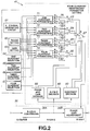
LPF 31 removes components of unneeded frequency bands of the imaging data offset by 1H as described above. TheYC matrix circuit 32 generates Y-signals and C-signals from the imaging data offset by 1H to route the generated Y-signals and C-signals to theRGB matrix circuit 33. TheRGB matrix circuit 33 generates red (R), green (G) and blue (B) color signals from the Y and C signals t route the respective color signals to thewhite balance circuit 34. For preventing picture deterioration during imaging of a white object at different color temperatures, the whitebalance adjustment circuit 34 adjusts the ratio of respective color signals obtained on imaging the white object to 1:1:1 to route the respective color signals to thegamma correction circuit 35. Thegamma correction circuit 35 gamma-corrects the R, G and B color signals to route the resulting signals to the phase/gain control circuit 36. The phase/gain control circuit 36 generates pre-set color difference signals from the respective color signals and adjusts the phase and the gain with the color difference signals as coordinate axes, by way of performing color signal adjustment, in a manner which will be subsequently explained in detail. Theblanking insertion circuit 37 pulls down the blanking period of the color-signal-adjusted color difference signals sufficiently below the black level to insert the blanking and routes the color difference signals to theencoder 38. Theencoder 38 generates C-signals of the NTSC (National television System Committee) system from the pre-set color difference signals and routes the resulting C-signals to thedelay circuit 39. Thedelay circuit 39 delays the C-signals in a pre-set amount for synchronization with the Y-signals and outputs the color-signal-adjusted C-signals via D/A converter 40. - Referring to Fig.2, the phase/
gain control circuit 36 includes an (R-G)/(B-G) convertingcircuit 36A for generating (R-G) signal and the (B-G) signal from the respective color signals of R, G and B and a phase/gain adjustment circuit 36B for generating (R-Y) and (B-Y) signals from the (R-G) and (B-G) signals in accordance with the following equations (1) and (2):
- X: gain of the (R-Y) signal
- Z: phase of the (R-Y) signal
- The (R-G)/(B-G)
conversion circuit 36A converts the respective color signals from thegamma correction circuit 35 into color difference (R-G) and (B-G) signals to route the color difference signals to a phase/gain adjustment circuit 36B. The phase/gain adjustment circuit 36B performs processing of the above equations, pixel by pixel, based on X and Z signals from thechroma SIO 41, as later explained, for generating (R-Y) and (B-Y) signals. - Similarly to the
luminance SIO 28, thechroma SIO 41 performs white balance and gamma correction in the C-signal processing unit 30, under control by the micro-computer 50, while generating X and Z signals and routing these signals to the phase/gain adjustment circuit 36B. - Specifically, the
chroma SIO 41 has an X.Zsignal generating circuit 61, aphase setting circuit 62, a gain setting circuit 63, a first quadrant selection circuit 64, a secondquadrant selection circuit 65, a thirdquadrant selection circuit 66 and a fourthquadrant selection circuit 67. - The X·Z
signal generating circuit 61 generates X and Z signals, required in the equations (1) and (2), under control by themicro-computer 50. - Responsive to the setting operation by the above-mentioned setting unit, the micro-computer 50 computes a gain XR of the (R-Y) signal, a phase ZR of the (R-Y) signal, a gain XB of the (B-Y) signal, and a phase ZB of the (B-Y) signal, for each of the first to fourth quadrants in the (B-Y) and (R-Y) coordinate systems, and routes the computed results to the X·Z
signal generating circuit 61. - Thus the X·Z
signal generating circuit 61 generates the gain signal XR1 and the phase signals ZR1 of the (R-Y) signals of the first quadrant, while generating the gain signal XB1 and the phase signals ZR1 of the (B-Y) signals of the first quadrant. Similarly, the X·Zsignal generating circuit 61 generates XR2, ZR2, XB2, ZB2 signals for the second quadrant, while generating XR3, ZR3, XB3 and ZB3 signals and XR4, ZR4, XB4 and ZB4 signals for the third and fourth quadrants, respectively. The X·Zsignal generating circuit 61 sends these X and Z signals to a firstquadrant parameter circuit 71, a secondquadrant parameter circuit 72, a thirdquadrant parameter circuit 73 and to a fourthquadrant parameter circuit 74. - If phase adjustment is turned off by the operation of the above operating unit, the
phase setting circuit 62 performs control, under control by the micro-computer 50, so that no Z-signals will be outputted by the firstquadrant parameter circuit 71, secondquadrant parameter circuit 72, thirdquadrant parameter circuit 73 nor fourthquadrant parameter circuit 74. - If phase adjustment is turned off by the operation of the above operating unit, the gain setting circuit 63 performs control, under control by the micro-computer 50, so that no X-signals will be outputted by the first
quadrant parameter circuit 71, secondquadrant parameter circuit 72, thirdquadrant parameter circuit 73 nor fourthquadrant parameter circuit 74. - If the above operating unit is actuated for performing the color signal adjustment of the first quadrant, the first quadrant selection circuit 64 controls the first
quadrant parameter circuit 71, under control by the micro-computer 50, for outputting X and Z signals supplied from the X·Zsignal generating circuit 61. - If the above operating unit is actuated for performing the color signal adjustment of the second quadrant, the second
quadrant selection circuit 65 controls the secondquadrant parameter circuit 72, under control by the micro-computer 50, for outputting X and Z signals supplied from the X·Zsignal generating circuit 61. - If the above operating unit is actuated for performing the color signal adjustment of the third quadrant, the third
quadrant selection circuit 66 controls the thirdquadrant parameter circuit 73, under control by the micro-computer 50, for outputting X and Z signals supplied from the X·Zsignal generating circuit 61. - If the above operating unit is actuated for performing the color signal adjustment of the fourth quadrant, the fourth
quadrant selection circuit 67 controls the thirdquadrant parameter circuit 74, under control by the micro-computer 50, for outputting X and Z signals supplied from the X·Zsignal generating circuit 61. - The
chroma SIO 41 has the above-mentioned first to fourthquadrant parameter circuits 71 to 74, switches 75 to 87, a phase/gain decision circuit 88, an (R-Y)/(B-Y)decision circuit 89 and aquadrant decision circuit 90. - Unless Z or X signals are set for not being outputted by the
phase setting circuit 62 or the gain setting circuit 63, the firstquadrant parameter circuit 71 outputs the XR1 signal, ZR1 signal, XB1 signal and the ZB1 signal from the X·Zsignal generating circuit 61 at terminals a, b, c and d, respectively. - Unless Z or X signals are set for not being outputted by the
phase setting circuit 62 or the gain setting circuit 63, the secondquadrant parameter circuit 72 outputs the XR2 signal, ZR2 signal, XB2 signal and the ZB2 signal from the X·Zsignal generating circuit 61 at terminals a, b, c and d, respectively. - Unless Z or X signals are set for not being outputted by the
phase setting circuit 62 or the gain setting circuit 63, the thirdquadrant parameter circuit 73 outputs the XR3 signal, ZR3 signal, XB3 signal and the ZB3 signal from the X·Zsignal generating circuit 61 at terminals a, b, c and d, respectively. - Unless Z or X signals are set for not being outputted by the
phase setting circuit 62 or the gain setting circuit 63, the fourthquadrant parameter circuit 74 outputs the XR4 signal, ZR4 signal, XB4 signal and the ZB4 signal from the X·Zsignal generating circuit 61 at terminals a, b, c and d, respectively. - The
switch 75 outputs signals from terminals a and b of the firstquadrant parameter circuit 71 under control by the phase/gain decision circuit 88. Theswitch 76 outputs signals from terminals c and d of the firstquadrant parameter circuit 71 under control by the phase/gain decision circuit 88. - The
switch 77 outputs signals from terminals a and b of the secondquadrant parameter circuit 72 under control by the phase/gain decision circuit 88. Theswitch 78 outputs signals from terminals c and d of the secondquadrant parameter circuit 72 under control by the phase/gain decision circuit 88. - The
switch 79 outputs signals from terminals a and b of the thirdquadrant parameter circuit 73 under control by the phase/gain decision circuit 88. The switch 80 outputs signals from terminals c and d of the thirdquadrant parameter circuit 73 under control by the phase/gain decision circuit 88. - The
switch 81 outputs signals from terminals a and b of the fourthquadrant parameter circuit 74 under control by the phase/gain decision circuit 88. Theswitch 82 outputs signals from terminals c and d of the fourthquadrant parameter circuit 74 under control by the phase/gain decision circuit 88. - The
switch 83 outputs signals from theswitch decision circuit 89. Similarly, theswitch 84 outputs signals from theswitch switch 79 or 80 and theswitch 86 outputs signals from theswitch - The
switch 87 outputs a signal from one of theswitches 83 to 86 under control by thequadrant decision circuit 90. - The phase/
gain decision circuit 88 controls the switching of theswitches 75 to 82 based on the (R-G) signal or the (B-G) signal supplied from the (R-G)/(B-G)conversion circuit 36A. - The phase/
gain decision circuit 88 judges whether the supplied signal is for conversion of the (R-Y) signal or (B-Y) signal and whether the supplied signal itself is the (R-G) signal or the (B-G) signal. If the phase/gain decision circuit 88 decides that the (R-G) signal for the (R-Y) signal conversion has been supplied, or that the (B-G) signal for (B-Y) signal conversion has been supplied, thedecision circuit 88 selects gain adjustment and sets theswitches switches gain decision circuit 88 decides that the (B-G) signal for (B-Y) signal conversion has been supplied, or that the (R-G) signal for (B-Y) signal conversion has been supplied, thedecision circuit 88 selects phase adjustment and sets theswitches switches - The (R-Y)/(B-Y)
decision circuit 89 judges whether the (R-G) signal or the (B-G) signal supplied from thegain control circuit 36 is for (R-Y) signal conversion or for (B-Y) conversion. The (R-Y)/(B-Y)decision circuit 89 sets theswitches 83 to 86 to the terminals e or f if the signal for (R-Y) signal conversion or the signal for (B-Y) signal conversion is supplied thereto, respectively. - The
quadrant decision circuit 90 judges in which quadrant the adjustment of the color difference signal of the gain/phase should be performed, and accordingly controls the switching of theswitch 87. For example, if the signs of the (R-G) signal and (B-G) signal are both {+}, thequadrant decision circuit 90 judges the color difference signal adjustment should be performed in the first quadrant. If the signs of the (R-G) signal and (B-G) signal are {+} and {-}, thequadrant decision circuit 90 judges the color difference signal adjustment should be performed in the second quadrant. If the signs of the (R-G) signal and (B-G) signal are {-} and {+}, thequadrant decision circuit 90 judges the color difference signal adjustment should be performed in the third quadrant. On the other hand, if the signs of the (R-G) signal and (B-G) signal are both {-}, thequadrant decision circuit 90 judges the color difference signal adjustment should be performed in the fourth quadrant. Thequadrant decision circuit 90 sets theswitch 87 to terminals g, h, i, or j if the conversion is in the first, second, third or fourth quadrant, respectively. The X and Z signals outputted by theswitch 87 are routed to the phase/gain adjustment circuit 36B. - That is, the
chroma SIO 41 generates a pre-set control signal, under control by the micro-computer 50, subject to the setting operation by the operating unit. Thechroma SIO 41 judges which of the phase processing or the gain processing is carried out at the time of conversion of the color difference signal in the phase/gain control circuit 36, which of the (R-Y) signal or the (B-Y) signal is controlled, or in which quadrant the adjustment is performed, and routes X and Z signals satisfying the above decision conditions pixel by pixel to the phase/gain adjustment circuit 36B. - Thus it is possible for the phase/
gain adjustment circuit 36B, fed with the X and Z signals for color signal adjustment from theswitch 87, to output (R-Y) and (B-Y) signals, which are optimally color-signal-adjusted color difference signals, at the time of conversion from the (R-G) and (B-G) signals to (R-Y) and (B-Y) signals. - As described above, it is possible for the color signal adjustment circuit of the present invention to judge the four parameters comprised of the positive and negative (R-G) and (B-G) signals before performing signal conversion of the color difference signals by the phase/
gain adjustment circuit 36B for deciding the gain X and the phase Z for performing color signal adjustment of the (R-Y) and (B-Y) signals. - Stated differently, with the above-described color signal adjustment circuit, the parameters required for conversion of the (R-Y) and (B-Y) signals may be reduced to one-half that required in the conventional circuit, thus contributing to improved communication speed between respective circuits.
- In addition, it is possible with the above-described color signal adjustment circuit to control conversion of the gain and the phase in the (B-Y) and (R-Y) coordinate system for each quadrant independently, such that there is no risk of color signal adjustment being made for a quadrant during color signal adjustment for another quadrant, while the gain and the phase for plural quadrants can be controlled simultaneously.
- Moreover, with the above-described color signal adjustment circuit, it is possible to adjust only the gain or only the phase in the above-mentioned coordinate system, while it is possible to set in which quadrant the gain adjustment or phase adjustment is performed, thus assisting the user in adjusting the color signals.
- Meanwhile, the color signal adjustment circuit includes the (R-G)/(B-G)
conversion circuit 36A, phase/gain adjustment circuit 36B,chroma SIO 41, (R-Y)/(B-Y) four-quadrant adjustment circuit 81 and the four-quadrant independentparameter setting unit 82 for enabling color signal adjustment to higher accuracy. Similarly to thechroma SIO 41, the four-quadrant independentparameter setting unit 82 adjusts the gain X and the phase Z of the (R-Y) and (B-Y) signals supplied to the (R-Y)/(B-Y) four-quadrant adjustment circuit 81. - Thus, with the above-described color signal adjustment circuit, since color signal adjustment is performed once in the (R-G)/(B-G)
conversion circuit 36A, phase/gain adjustment circuit 36B and in thechroma SIO 41, the gain X and the phase Z are then again set in the four-quadrant independentparameter setting unit 82 and subsequently the (R-Y) and (B-Y) signals are outputted by the (R-Y)/(B-Y) four-quadrant adjustment circuit 81, thus achieving color signal adjustment to higher precision.
Claims (3)
- A color signal adjustment apparatus comprising:first color difference signal generating means for generating a (R-G) signal and a (B-G) signal from R, G and B signals;second color difference generating means for generating, in a (B-Y) - (B-G) coordinate system having a (B-Y) signal and an (R-Y) signal as an abscissa and an ordinate, respectively, the (R-Y) signal and the (B-Y) signal, using the (R-G) signal and the (B-G) signal from said first color difference signal generating means, in accordance with the following equations:
 X: gain of the (R-Y) signalZ: phase of the (R-Y) signal; and
 X: gain of the (B-Y) signalZ: phase of the (B-Y) signal;first parameter outputting means for outputting a gain and a phase for the (R-Y) signal and a gain and a phase for the (B-Y) signal in the first quadrant in said (B-Y) - (R-Y) coordinate system;second parameter outputting means for outputting a gain and a phase for the (R-Y) signal and a gain and a phase for the (B-Y) signal in the second quadrant in said (B-Y) - (R-Y) coordinate system;third parameter outputting means for outputting a gain and a phase for the (R-Y) signal and a gain and a phase for the (B-Y) signal in the third quadrant in said (B-Y) - (R-Y) coordinate system;fourth parameter outputting means for outputting a gain and a phase for the (R-Y) signal and a gain and a phase for the (B-Y) signal in the fourth quadrant in said (B-Y) - (R-Y) coordinate system;selection means for switchingly selecting the gain or the phase from one of said first parameter setting means, second parameter setting means, third parameter setting means and the fourth parameter setting means, and sending the selected gain or phase to said second color difference generating means; andcontrol means for controlling said selection means based on the (R-G) signal and the (B-G) signal from said first color difference signal generating means.
 - The color signal adjustment apparatus as claimed in claim 1 wherein said control means controlssaid switching means for outputting the gain for the (R-Y) signal of the first quadrant if the signs of the (R-G) signal and the (B-G) signal from the first color difference generating means are both positive and if said (R-G) signal and the (B-G) signal indicate the gain for the (R-Y) signal; said control means controllingsaid switching means for outputting the gain for the (B-Y) signal of the first quadrant if the signs of the (R-G) signal and the (B-G) signal from the first color difference generating means are both positive and if said (R-G) signal and the (B-G) signal indicate the gain for the (B-Y) signal; said switching means controllingsaid switching means for outputting the phase for the (R-Y) signal of the first quadrant if the signs of the (R-G) signal and the (B-G) signal from the first color difference generating means are both positive and if said (R-G) signal and the (B-G) signal indicate the phase for the (R-Y) signal; said switching means controllingsaid switching means for outputting the phase for the (B-Y) signal of the first quadrant if the signs of the (R-G) signal and the (B-G) signal from the first color difference generating means are both positive and if said (R-G) signal and the (B-G) signal indicate the phase for the (B-Y) signal; said control means controllingsaid switching means for outputting the gain for the (R-Y) signal of the second quadrant if the signs of the (R-G) signal and the (B-G) signal from the first color difference generating means are positive and negative, respectively, and if said (R-G) signal and the (B-G) signal indicate the gain for the (R-Y) signal; said control means controllingsaid switching means for outputting the gain for the (B-Y) signal of the second quadrant if the signs of the (R-G) signal and the (B-G) signal from the first color difference generating means are positive and negative, respectively, and if said (R-G) signal and the (B-G) signal indicate the gain for the (B-Y) signal; said control means controllingsaid switching means for outputting the phase for the (R-Y) signal of the second quadrant if the signs of the (R-G) signal and the (B-G) signal from the first color difference generating means are positive and negative, respectively, and if said (R-G) signal and the (B-G) signal indicate the phase for the (R-Y) signal; said control means controllingsaid switching means for outputting the gain for the (B-Y) signal of the second quadrant if the signs of the (R-G) signal and the (B-G) signal from the first color difference generating means are positive and negative, respectively, and if said (R-G) signal and the (B-G) signal indicate the phase for the (B-Y) signal; said control means controllingsaid switching means for outputting the gain for the (R-Y) signal of the third quadrant if the signs of the (R-G) signal and the (B-G) signal from the first color difference generating means are both negative and if said (R-G) signal and the (B-G) signal indicate the gain for the (R-Y) signal; said control means controllingsaid switching means for outputting the gain for the (B-Y) signal of the third quadrant if the signs of the (R-G) signal and the (B-G) signal from the first color difference generating means are both negative and if said (R-G) signal and the (B-G) signal indicate the gain for the (B-Y) signal; said switching means controllingsaid switching means for outputting the phase for the (R-Y) signal of the third quadrant if the signs of the (R-G) signal and the (B-G) signal from the first color difference generating means are both negative and if said (R-G) signal and the (B-G) signal indicate the phase for the (R-Y) signal; said switching means controllingsaid switching means for outputting the phase for the (B-Y) signal of the third quadrant if the signs of the (R-G) signal and the (B-G) signal from the first color difference generating means are both negative and if said (R-G) signal and the (B-G) signal indicate the phase for the (B-Y) signal; said control means controllingsaid switching means for outputting the gain for the (R-Y) signal of the fourth quadrant if the signs of the (R-G) signal and the (B-G) signal from the first color difference generating means are negative and positive, respectively, and if said (R-G) signal and the (B-G) signal indicate the gain for the (R-Y) signal; said control means controllingsaid switching means for outputting the gain for the (B-Y) signal of the fourth quadrant if the signs of the (R-G) signal and the (B-G) signal from the first color difference generating means are negative and positive, respectively, and if said (R-G) signal and the (B-G) signal indicate the gain for the (B-Y) signal; said control means controllingsaid switching means for outputting the phase for the (R-Y) signal of the fourth quadrant if the signs of the (R-G) signal and the (B-G) signal from the first color difference generating means are negative and positive, respectively, and if said (R-G) signal and the (B-G) signal indicate the phase for the (R-Y) signal; said control means controllingsaid switching means for outputting the phase for the (B-Y) signal of the fourth quadrant if the signs of the (R-G) signal and the (B-G) signal from the first color difference generating means are negative and positive, respectively, and if said (R-G) signal and the (B-G) signal indicate the phase for the (B-Y) signal.
- The color signal adjustment apparatus as claimed in claim 1 wherein said selection means includesfirst selection means for switchingly selecting said first parameter outputting means, second parameter outputting means, third parameter outputting means or said fourth parameter outputting means;second selection means for switchingly selecting the gain or the phase of the (R-Y) signal and the (B-Y) signal outputted by said first parameter outputting means, the gain or the phase of the (R-Y) signal and the (B-Y) signal outputted by said second parameter outputting means, the gain or the phase of the (R-Y) signal and the (B-Y) signal outputted by said third parameter outputting means, or the gain or the phase of the (R-Y) signal and the (B-Y) signal outputted by said fourth parameter outputting means; andthird selection means for switchingly selecting the gain and the phase of the (R-Y) signal or the (B-Y) signal outputted by said first parameter outputting means, the gain and the phase of the (R-Y) signal or the (B-Y) signal outputted by said second parameter outputting means, the gain and the phase of the (R-Y) signal or the (B-Y) signal outputted by said third parameter outputting means, or the gain and the phase of the (R-Y) signal or the (B-Y) signal outputted by said fourth parameter outputting means.
Applications Claiming Priority (3)
| Application Number | Priority Date | Filing Date | Title |
|---|---|---|---|
| JP32516/96 | 1996-02-20 | ||
| JP03251696A JP3724038B2 (en) | 1996-02-20 | 1996-02-20 | Color signal adjusting device and camera device |
| JP3251696 | 1996-02-20 |
Publications (3)
| Publication Number | Publication Date |
|---|---|
| EP0792073A2 true EP0792073A2 (en) | 1997-08-27 |
| EP0792073A3 EP0792073A3 (en) | 1997-11-26 |
| EP0792073B1 EP0792073B1 (en) | 2002-01-16 |
Family
ID=12361143
Family Applications (1)
| Application Number | Title | Priority Date | Filing Date |
|---|---|---|---|
| EP97301004A Expired - Lifetime EP0792073B1 (en) | 1996-02-20 | 1997-02-17 | Color signal adjustment apparatus |
Country Status (6)
| Country | Link |
|---|---|
| US (1) | US6040855A (en) |
| EP (1) | EP0792073B1 (en) |
| JP (1) | JP3724038B2 (en) |
| KR (1) | KR100442160B1 (en) |
| DE (1) | DE69709557T2 (en) |
| MY (1) | MY115525A (en) |
Families Citing this family (2)
| Publication number | Priority date | Publication date | Assignee | Title |
|---|---|---|---|---|
| US6798449B2 (en) * | 2001-01-18 | 2004-09-28 | Kinpo Electronics, Inc. | Automatic white-balance correction for digital camera |
| JP4156631B2 (en) * | 2006-04-26 | 2008-09-24 | シャープ株式会社 | Image processing method and image processing apparatus |
Citations (3)
| Publication number | Priority date | Publication date | Assignee | Title |
|---|---|---|---|---|
| DE1916690B2 (en) * | 1968-04-01 | 1974-07-04 | Rca Corp., New York, N.Y. (V.St.A.) | Color coding matrix |
| GB2208460A (en) * | 1987-07-24 | 1989-03-30 | Nippon Denki Home Electronics | Color signal compensating system |
| US5272523A (en) * | 1991-12-31 | 1993-12-21 | Samsung Electronics Co., Ltd. | Matrix circuit for separating color signal of a video camera into color-difference signals |
Family Cites Families (3)
| Publication number | Priority date | Publication date | Assignee | Title |
|---|---|---|---|---|
| US3662097A (en) * | 1970-05-18 | 1972-05-09 | Zenith Radio Corp | Chroma processing circuitry with selectable color correction mode |
| US4364080A (en) * | 1981-04-13 | 1982-12-14 | Jovan Vidovic | Digital video analyzer |
| JP3253125B2 (en) * | 1991-07-04 | 2002-02-04 | 株式会社東芝 | Color image reading correction device |
-
1996
- 1996-02-20 JP JP03251696A patent/JP3724038B2/en not_active Expired - Fee Related
-
1997
- 1997-02-17 EP EP97301004A patent/EP0792073B1/en not_active Expired - Lifetime
- 1997-02-17 DE DE69709557T patent/DE69709557T2/en not_active Expired - Lifetime
- 1997-02-18 MY MYPI97000579A patent/MY115525A/en unknown
- 1997-02-18 US US08/801,519 patent/US6040855A/en not_active Expired - Lifetime
- 1997-02-20 KR KR1019970005118A patent/KR100442160B1/en not_active IP Right Cessation
Patent Citations (3)
| Publication number | Priority date | Publication date | Assignee | Title |
|---|---|---|---|---|
| DE1916690B2 (en) * | 1968-04-01 | 1974-07-04 | Rca Corp., New York, N.Y. (V.St.A.) | Color coding matrix |
| GB2208460A (en) * | 1987-07-24 | 1989-03-30 | Nippon Denki Home Electronics | Color signal compensating system |
| US5272523A (en) * | 1991-12-31 | 1993-12-21 | Samsung Electronics Co., Ltd. | Matrix circuit for separating color signal of a video camera into color-difference signals |
Non-Patent Citations (1)
| Title |
|---|
| JOURNAL OF THE SMPTE, vol. 78, no. 9, September 1969, pages 696-700, XP002040858 MONAHAN,DISCHERT: "color correction techniques for television cameras" * |
Also Published As
| Publication number | Publication date |
|---|---|
| JPH09233491A (en) | 1997-09-05 |
| EP0792073A3 (en) | 1997-11-26 |
| JP3724038B2 (en) | 2005-12-07 |
| EP0792073B1 (en) | 2002-01-16 |
| US6040855A (en) | 2000-03-21 |
| KR100442160B1 (en) | 2004-10-28 |
| KR970064278A (en) | 1997-09-12 |
| DE69709557T2 (en) | 2002-08-22 |
| DE69709557D1 (en) | 2002-02-21 |
| MY115525A (en) | 2003-07-31 |
Similar Documents
| Publication | Publication Date | Title |
|---|---|---|
| US6204878B1 (en) | Image pickup device having interlacing circuitry | |
| EP0713342B1 (en) | Color image sensing apparatus and method of expanding dynamic range | |
| CA2252183C (en) | An imaging apparatus with dynamic range expanded, a video camera including the same, and a method of generating a dynamic range expanded video signal | |
| US5548330A (en) | Image pickup device for generating a corrected luminance signal | |
| US6353488B1 (en) | Image sensing apparatus having common circuitry for processing digital adjustment signals | |
| US5481317A (en) | Gamma correction circuit which selects one of a plurality of gamma corrected signals as an output signal based on the level of an input signal | |
| EP0521367B1 (en) | Video signal processing circuit | |
| US5170249A (en) | Digital signal processing apparatus having devices for delaying and combining color signals | |
| US6147707A (en) | Method and apparatus for gain adjustment of an image sensor | |
| EP0516460B1 (en) | Digital signal processing system for color camera apparatus | |
| EP0705516B1 (en) | High luminance color suppression circuit | |
| JP3583952B2 (en) | Black and white / color switching camera | |
| EP0558338B1 (en) | Video camera | |
| JPS59193684A (en) | Negative/positive inverting device | |
| KR910006858B1 (en) | Picture image processing circuit of color camera | |
| US6690418B1 (en) | Image sensing apparatus image signal controller and method | |
| KR20000041319A (en) | Apparatus for processing color signal of image signal processing system | |
| KR950008129B1 (en) | Pick-up device with whit-balance control improved | |
| EP0792073B1 (en) | Color signal adjustment apparatus | |
| EP0746166A2 (en) | Image sensing apparatus and method | |
| US5912702A (en) | Video camera and image enhancing apparatus | |
| JPH09224186A (en) | Video camera and control correcting device | |
| EP0620692B1 (en) | Tint detection circuit | |
| JP2569492B2 (en) | Video camera | |
| KR0176843B1 (en) | Auto-color balance and its control method |
Legal Events
| Date | Code | Title | Description |
|---|---|---|---|
| PUAI | Public reference made under article 153(3) epc to a published international application that has entered the european phase |
Free format text: ORIGINAL CODE: 0009012 |
|
| AK | Designated contracting states |
Kind code of ref document: A2 Designated state(s): DE FR GB |
|
| PUAL | Search report despatched |
Free format text: ORIGINAL CODE: 0009013 |
|
| AK | Designated contracting states |
Kind code of ref document: A3 Designated state(s): DE FR GB |
|
| 17P | Request for examination filed |
Effective date: 19980421 |
|
| GRAG | Despatch of communication of intention to grant |
Free format text: ORIGINAL CODE: EPIDOS AGRA |
|
| 17Q | First examination report despatched |
Effective date: 20010314 |
|
| GRAG | Despatch of communication of intention to grant |
Free format text: ORIGINAL CODE: EPIDOS AGRA |
|
| GRAH | Despatch of communication of intention to grant a patent |
Free format text: ORIGINAL CODE: EPIDOS IGRA |
|
| GRAH | Despatch of communication of intention to grant a patent |
Free format text: ORIGINAL CODE: EPIDOS IGRA |
|
| GRAA | (expected) grant |
Free format text: ORIGINAL CODE: 0009210 |
|
| REG | Reference to a national code |
Ref country code: GB Ref legal event code: IF02 |
|
| AK | Designated contracting states |
Kind code of ref document: B1 Designated state(s): DE FR GB |
|
| REF | Corresponds to: |
Ref document number: 69709557 Country of ref document: DE Date of ref document: 20020221 |
|
| ET | Fr: translation filed | ||
| PLBE | No opposition filed within time limit |
Free format text: ORIGINAL CODE: 0009261 |
|
| STAA | Information on the status of an ep patent application or granted ep patent |
Free format text: STATUS: NO OPPOSITION FILED WITHIN TIME LIMIT |
|
| 26N | No opposition filed | ||
| PGFP | Annual fee paid to national office [announced via postgrant information from national office to epo] |
Ref country code: FR Payment date: 20120227 Year of fee payment: 16 |
|
| PGFP | Annual fee paid to national office [announced via postgrant information from national office to epo] |
Ref country code: DE Payment date: 20120221 Year of fee payment: 16 |
|
| PGFP | Annual fee paid to national office [announced via postgrant information from national office to epo] |
Ref country code: GB Payment date: 20120221 Year of fee payment: 16 |
|
| REG | Reference to a national code |
Ref country code: GB Ref legal event code: 746 Effective date: 20120703 |
|
| REG | Reference to a national code |
Ref country code: DE Ref legal event code: R084 Ref document number: 69709557 Country of ref document: DE Effective date: 20120614 |
|
| GBPC | Gb: european patent ceased through non-payment of renewal fee |
Effective date: 20130217 |
|
| REG | Reference to a national code |
Ref country code: FR Ref legal event code: ST Effective date: 20131031 |
|
| REG | Reference to a national code |
Ref country code: DE Ref legal event code: R119 Ref document number: 69709557 Country of ref document: DE Effective date: 20130903 |
|
| PG25 | Lapsed in a contracting state [announced via postgrant information from national office to epo] |
Ref country code: GB Free format text: LAPSE BECAUSE OF NON-PAYMENT OF DUE FEES Effective date: 20130217 Ref country code: FR Free format text: LAPSE BECAUSE OF NON-PAYMENT OF DUE FEES Effective date: 20130228 Ref country code: DE Free format text: LAPSE BECAUSE OF NON-PAYMENT OF DUE FEES Effective date: 20130903 |