EP0788108B1 - Synchronous semi-conductor memory device - Google Patents
Synchronous semi-conductor memory device Download PDFInfo
- Publication number
- EP0788108B1 EP0788108B1 EP97101364A EP97101364A EP0788108B1 EP 0788108 B1 EP0788108 B1 EP 0788108B1 EP 97101364 A EP97101364 A EP 97101364A EP 97101364 A EP97101364 A EP 97101364A EP 0788108 B1 EP0788108 B1 EP 0788108B1
- Authority
- EP
- European Patent Office
- Prior art keywords
- signal
- data
- output
- circuit
- latch
- Prior art date
- Legal status (The legal status is an assumption and is not a legal conclusion. Google has not performed a legal analysis and makes no representation as to the accuracy of the status listed.)
- Expired - Lifetime
Links
- 239000004065 semiconductor Substances 0.000 title claims description 21
- 230000001360 synchronised effect Effects 0.000 title description 5
- 230000004044 response Effects 0.000 claims description 9
- 102100035606 Beta-casein Human genes 0.000 claims description 3
- 101000947120 Homo sapiens Beta-casein Proteins 0.000 claims description 3
- 230000000295 complement effect Effects 0.000 claims description 3
- 238000010586 diagram Methods 0.000 description 10
- 238000005457 optimization Methods 0.000 description 3
- 230000003213 activating effect Effects 0.000 description 2
- 239000000470 constituent Substances 0.000 description 2
- 230000000415 inactivating effect Effects 0.000 description 2
- 201000008103 leukocyte adhesion deficiency 3 Diseases 0.000 description 2
- 238000004519 manufacturing process Methods 0.000 description 2
- 239000004020 conductor Substances 0.000 description 1
- 230000003111 delayed effect Effects 0.000 description 1
- 238000000034 method Methods 0.000 description 1
- 238000009877 rendering Methods 0.000 description 1
- 230000000717 retained effect Effects 0.000 description 1
Images


Classifications
-
- G—PHYSICS
- G11—INFORMATION STORAGE
- G11C—STATIC STORES
- G11C11/00—Digital stores characterised by the use of particular electric or magnetic storage elements; Storage elements therefor
- G11C11/21—Digital stores characterised by the use of particular electric or magnetic storage elements; Storage elements therefor using electric elements
- G11C11/34—Digital stores characterised by the use of particular electric or magnetic storage elements; Storage elements therefor using electric elements using semiconductor devices
- G11C11/40—Digital stores characterised by the use of particular electric or magnetic storage elements; Storage elements therefor using electric elements using semiconductor devices using transistors
- G11C11/401—Digital stores characterised by the use of particular electric or magnetic storage elements; Storage elements therefor using electric elements using semiconductor devices using transistors forming cells needing refreshing or charge regeneration, i.e. dynamic cells
-
- G—PHYSICS
- G11—INFORMATION STORAGE
- G11C—STATIC STORES
- G11C7/00—Arrangements for writing information into, or reading information out from, a digital store
- G11C7/10—Input/output [I/O] data interface arrangements, e.g. I/O data control circuits, I/O data buffers
- G11C7/1051—Data output circuits, e.g. read-out amplifiers, data output buffers, data output registers, data output level conversion circuits
- G11C7/106—Data output latches
-
- G—PHYSICS
- G11—INFORMATION STORAGE
- G11C—STATIC STORES
- G11C7/00—Arrangements for writing information into, or reading information out from, a digital store
- G11C7/10—Input/output [I/O] data interface arrangements, e.g. I/O data control circuits, I/O data buffers
- G11C7/1051—Data output circuits, e.g. read-out amplifiers, data output buffers, data output registers, data output level conversion circuits
-
- G—PHYSICS
- G11—INFORMATION STORAGE
- G11C—STATIC STORES
- G11C7/00—Arrangements for writing information into, or reading information out from, a digital store
- G11C7/10—Input/output [I/O] data interface arrangements, e.g. I/O data control circuits, I/O data buffers
- G11C7/1051—Data output circuits, e.g. read-out amplifiers, data output buffers, data output registers, data output level conversion circuits
- G11C7/1069—I/O lines read out arrangements
Definitions
- This invention relates to a semiconductor memory device, and in particular to a synchronous semiconductor memory device having an internal pipeline structure.
- a synchronous semiconductor memory device having an internal pipeline structure has been proposed by, for example, Japanese Laid-Open (Kokai) Patent Publication Sho 61-148692, Japanese Laid-Open (Kokai) Patent Publication Hei 6-76566, or Japanese Laid-Open (Kokai) Patent Publication 8-96573.
- this semiconductor memory device includes an input circuit 1 having a set of address terminals ADD, an input circuit 2 having a mask signal terminal DQM, and an input circuit 3 having a clock terminal CLK, which responds to an external clock CLK and outputs an internal synchronizing signal ⁇ 1.
- a burst counter 4 receives the output from the input circuits 1 and outputs a plurality of internal address signals IADD in synchronization with the internal synchronizing signal ⁇ 1.
- a column decoder 5 receives the internal address signals IADD and outputs a set column selective lines YSW to a sense amplifier circuit 7 coupled to a cell array 6 including a plurality of memory cells (not shown). The sense amplifier circuit 7 thus outputs the data from the selected memory cells of the cell array 6 while amplifying the data.
- a synchronizing signal-generating circuit 8 responds to the internal synchronizing signal ⁇ 1 to produce an internal synchronizing signal ⁇ 2, and a synchronizing signal-generating circuit 9 also responds to the internal synchronizing signal ⁇ 1 to produce an internal synchronizing signal ⁇ 3.
- a set of latch circuits 10 latching the data from the sense amplifiers 7 and outputting the latched data in synchronism with the internal synchronizing signal ⁇ 2, which is in turn supplied to a data amplifiers 24.
- the data D1 from the amplifier 25 is supplied to a D-F/F circuit 25 which in turn fetches the data D1 and outputs data D2 in synchronism with the internal synchronizing signal ⁇ 3.
- a latch circuit 12 is further provided for receiving the output from the input circuit 2 and outputting a mask signal MSK1B in synchronism with the internal synchronizing signal ⁇ 1.
- a D-F/F circuit 27 receives the output from the latch circuit 12 and outputs a signal in synchronism with the internal synchronizing signal ⁇ 1, which signal is delayed by a delay element DL and produced as a mask signal MSK2B.
- This signal MSK2B and the data D2 are supplied to an output control circuit 26 includes gates AN3 and AN4, the output signals D3T and D3N are in turn supplied to an output circuit 17 to drive an output terminal DQ by use of transistors Tr1 and Tr2.
- the output control circuit 26 is composed of the AND gate AN3 for inputting the data D2 and the mask signal MSK2B and outputting conduction control signals D3T, and the AND gate AN4 for inputting a reversed signal of the data D2 and the mask signal MSK2B and outputting conduction control signals D3N.
- the mask signal MSK2B to be input in this case is an output control signal for controlling whether the output terminal DQ of the output circuit. 17 should be actuated or put into a high impedance.
- the output control circuit 26 is designed to output a signal by activating one of the conduction control signals D3T and D3N or by inactivating each of the conductor control signals D3T and D3N in accordance with the mask signal MSK2B and the data D2.
- the output circuit 17 is composed of an N-channel output transistor Tr1 which is connected between a power source and the output terminal DQ, the gate thereof being constituted by the conduction control signal D3T, and another N-channel output transistor Tr2 which is connected between the output terminal DQ and the ground, the gate thereof being constituted by the conduction control signal D3N.
- the output circuit 17 is so designed that it outputs a high level of signal by actuating the output terminal DQ when only the conduction control signal D3T is activated, While it outputs a low level of signal by actuating the output terminal DQ when only the conduction control signal D3N is activated.
- the output terminal DQ is set into the state of high impedance.
- burst indicates a continuous reading of data of any number of bits by the input of one read command. Therefore, at the burst counter 4, an internal address corresponding to "burst length" is produced.
- the internal synchronizing signal ⁇ 1 is changed to the high level, so that a high level of pulse is also generated in each of the internal synchronizing signals ⁇ 2 and ⁇ 3.
- the mask signal MSK1B becomes level low in synchronism with the internal synchronizing signal ⁇ 1 of this cycle.
- the internal synchronism signal ⁇ 3 is shifted from the low level to the high level, the mask signal MSK2B becomes low in level after a predetermined delay of the delay element DL.
- the data R2 corresponding to the cycle C2 is output at first as the data D1 from the data amplifier 24 in synchronism with the internal synchronizing signal ⁇ 2, and then as the data D2 from the D-F/F circuit 25 in synchronism with the internal synchronizing signal ⁇ 3.
- the data R2 is also transmitted in conformity with the data D2 to the conduction control signals D3T and D3N of the output control circuit 14.
- the conduction control signals D3T and D3N becomes also low in level.
- both of N-channel output transistors Tr1 and TR2 in the output circuit 17 are turned OFF, thus rendering the output terminal DQ in a state of high impedance (Hi-Z).
- the mask signal MSK1B becomes high in level in synchronism with the internal synchronizing signal ⁇ 1 of this cycle.
- the mask signal MSK2B becomes high in level after a predetermined delay of the delay element DL. Therefore, the data R3 is transmitted in conformity with the data D2 to the conduction control signals D3T and D3N of the output control circuit 14-16. As a result, one of N-channel output transistors Tr1 and and Tr2 is turned ON, and hence the data R3 is supplied to the output terminal DQ.
- the time interval starting from the state of high level of the external clock CLK at the cycle 3 to the time when the output terminal DQ is turned into a state of high impedance (Hi-Z) is prescribed as a critical value called tHZ. Accordingly, the output terminal DQ is required to be turned into a state of high impedance (Hi-Z) earlier than the critical value tHZ. Moreover, the data R1 being supplied to the output terminal DQ after the external clock-CLK at the cycle C3 is turned into a high level is required to be retained for a time period longer than that prescribed by the critical value tOH.
- the timing for turning the output terminal DQ into a state of high impedance (Hi-Z) after the input of the mask command is determined by the delay time of the delay element DL for outputting the mask signal MSK2B, i.e. an output control signal. For this reason, if this delay time is too short, the output terminal DQ is turned into a state of high impedance (Hi-Z) too fast, thus badly affecting the critical value tOH. On the other hand, if this delay time is too long, the output terminal DQ is turned into a state of high impedance (Hi-Z) too late, thus badly affecting the critical value tHZ. Therefore, the optimization of the delay time of the delay element DL is very important.
- a semiconductor memory device corresponding to the preamble part of the main claim is known from EP-A-0 427 286.
- a data amplifier 11 receives the output from the latch circuit 10 and producing a true data signal D1T and a complementary data signal D1N indicative of the received data. These signals D1T and D1N are supplied to an output control circuit 14 together with the mask signal MSK2B from D-F/F circuit 13 which responds to the change of the signal ⁇ 3 from the high to low level.
- the output control circuit 14 In response to these signals, the output control circuit 14 produces conduction control signals D2T and D2N which are in turn supplied to D-F/F circuits 15 and 16, respectively. These circuits 15 and 16 catch the conduction control signals D2T and D2N in synchronism with the internal synchronizing signal ⁇ 3 and produce drive control signals D3T and D3N, respectively. In response to these signals D3T and D3N, an output circuit 17 drives an output terminal DQ.
- the output control circuit 14 is composed of an AND gate AN1 supplied with the data signal D1T and the mask signal MSK2B and outputting the conduction control signal D2T, and an AND gate AN2 supplied with the data signal D1N and the mask signal MSK2B and outputting the conduction control signal D2N.
- the mask signal MSK2B to be input in this case is an output control signal for controlling whether the output terminal DQ of the output circuit 17 should be actuated or put into a high impedance.
- the output control circuit 14 is designed to output a signal by activating one of the conduction control signals D2T and D2N or by inactivating each of the conduction control signals D2T and D2N in accordance with the mask signal MSK2B and the data signals D1T and D1N.
- the output circuit 17 is composed of an N-channel output transistor Tr1 connected between a power source and the output terminal DQ, the gate thereof being supplied with the conduction control signal D3T, and an N-channel output transistor Tr2 connected between the output terminal DQ and the ground, the gate thereof being supplied with the conduction control signal D3N.
- the output circuit 17 is so designed that it outputs a high level of signal by actuating the output terminal DQ when the conduction control signal D3T is activated, i.e. the high level, while it outputs a low level of signal by actuating the output terminal DQ when the conduction control signal D3N is activated, i.e. the high level.
- the conduction control signals D3T and D3N are both being inactivated, i.e., the low level, the output terminal DQ is brought into a state of high impedance.
- the mask signal MSK1B becomes low in level in synchronism with the internal synchronizing signsl ⁇ 1 of this cycle.
- the internal synchronizing signal ⁇ 3 is shifted from a high level to a low level, the mask signal MSK2B becomes low in level.
- the data R2 corresponding to the cycle C2 is produced at first as the data D1T and D1N from the data amplifier 11 in synchronism with the internal synchronizing signal ⁇ 2, and thereafter the conduction control signals D2T and D2N are produced from the output control circuit 14.
- the output control circuit 14 changes each of the outputs D2T and D2N to the low level irrespective of the data R2. Accordingly, the output terminal DQ is not driven by the data R2, but brought into a state of high impedance (Hi-Z).
- the mask signal MSK1B becomes high in level in synchronism with the internal synchronizing signal ⁇ 1 of this cycle.
- the mask signal MSK2B becomes high.
- the data R3 complying with the cycle 3 is output as the data D1T/N from the data amplifier 11 in synchronism with the internal synchronizing signal ⁇ 2.
- the mask signal MSK2B becomes high in level by the change of the signal ⁇ 3 from the high level to the low level. Accordingly, the conduction control signals D2T and D2N take the respective levels responsive to the data R3.
- FIG. 3 there is shown a memory device according to another embodiment of this invention, in which the same constituents as those shown in FIG. 1 are denoted by the same reference numerals to omit the further description thereof.
- this memory there are provided an input circuit 18 receiving a row address strobe signal RASB, an input circuit 19 receiving a column address strobe signal CASB, an input circuit 20 receiving a write-enable signal WEB, and an input circuit 21 receiving a chip-select signal CSB.
- These signals are then supplied to a command decoder 22 whose output signal is in turn applied to a latch circuit 23 controlled by the signal ⁇ 1.
- the output of the latch circuit 23 is led out as a read signal READB and supplied to the F/F circuit 13.
- the output signal of the F/F circuit 13 is led out as an output-enable signal OEB in this embodiment, which is in turn supplied to the output control circuit 14.
- the signals RASB, CASB, WEB and CSB are supplied with a logic combination indicative of a read command at the cycle C1, this logic combination is decoded by the decoder 22.
- the read signal READB thereby becomes high in level in synchronism with the internal synchronizing signal ⁇ 1 in the next cycle C2.
- the output-enable signal OEB becomes high in level.
- the signal OEB is held at the low level at the timing when the signal ⁇ 3 is changed to the high level. Accordingly, the data R1 does not appear at the output terminal DQ in the cycle C2.
- the control signal D2T and D2N take the respective levels responsive to the data R1 in the cycle C3. Accordingly, the high level of the internal synchronizing signal ⁇ 3 in the cycle C3 has the F/F circuits 15 and 16 catch the signals D2T and D2N, respectively. As a result, one of the output transistors Tr1 and Tr2 is turned ON to drive the output terminal DQ at the level corresponding to the data R1.
- the read signal READB becomes low in level in synchronization with the internal synchronizing signal ⁇ 1 of the cycle C4, and when the internal synchronizing signal ⁇ 3 is shifted from the high level to the low level in the cycle C4, the output-enable signal OEB is turned to the low level. Accordingly, the data R2 appears at the output terminal DQ in the cycle C4, but the output terminal DQ is brought into the high impedance state in the cycle C5.
- the semiconductor memory device is provided with a plurality of latching circuits, each adapted to individually latch and output a conduction control signal in synchronization with an internal synchronizing signal of controlling the internal pipe line, and each of the output transistors of the output circuit is separately controlled in accordance with the output of each of said latching circuits. Therefore, the non-uniformity in delay of time interval from the input of the internal synchronizing signal into each latching circuit to each output transistor can be minimized, so that all of the output terminals can be actuated with the same timing to take a high level or a low level, or to be put into the state of a high impedance. Accordingly, the optimization of the relevant specified timing values (tHZ, tOH) can be easily performed.
- the non-uniformity of delay can be minimized as explained above, the fluctuation due to non-uniformity in product and the changes in voltage of power source can be also minimized, so that the characteristic obtainable by the relevant specified timing values can be further improved.
Landscapes
- Engineering & Computer Science (AREA)
- Microelectronics & Electronic Packaging (AREA)
- Computer Hardware Design (AREA)
- Dram (AREA)
- Static Random-Access Memory (AREA)
- Semiconductor Memories (AREA)
Description
- This invention relates to a semiconductor memory device, and in particular to a synchronous semiconductor memory device having an internal pipeline structure.
- With an advancement of a high-speed CPU in recent years, there has been a strong demand for a semiconductor memory device of higher speed. However, due to physical limitations to the miniaturization in the process of manufacturing the device or due to an enlargement of chip size resulting from a trend to increase the capacity of the device, such a demand is not necessarily fulfilled as yet.
- Under the circumstances, as a means to solve this problem, a synchronous semiconductor memory device having an internal pipeline structure has been proposed by, for example, Japanese Laid-Open (Kokai) Patent Publication Sho 61-148692, Japanese Laid-Open (Kokai) Patent Publication Hei 6-76566, or Japanese Laid-Open (Kokai) Patent Publication 8-96573.
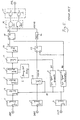
- Referring now to Fig. 5, such a conventional semiconductor memory device is shown as a block diagram. this semiconductor memory device includes an
input circuit 1 having a set of address terminals ADD, aninput circuit 2 having a mask signal terminal DQM, and aninput circuit 3 having a clock terminal CLK, which responds to an external clock CLK and outputs an internal synchronizing signal 1. Aburst counter 4 receives the output from theinput circuits 1 and outputs a plurality of internal address signals IADD in synchronization with the internal synchronizing signal 1. A column decoder 5 receives the internal address signals IADD and outputs a set column selective lines YSW to a sense amplifier circuit 7 coupled to acell array 6 including a plurality of memory cells (not shown). The sense amplifier circuit 7 thus outputs the data from the selected memory cells of thecell array 6 while amplifying the data. - On the other hand, a synchronizing signal-generating circuit 8 responds to the internal synchronizing signal 1 to produce an internal synchronizing signal 2, and a synchronizing signal-generating
circuit 9 also responds to the internal synchronizing signal 1 to produce an internal synchronizing signal 3. There are further provided a set oflatch circuits 10 latching the data from the sense amplifiers 7 and outputting the latched data in synchronism with the internal synchronizing signal 2, which is in turn supplied to adata amplifiers 24. The data D1 from theamplifier 25 is supplied to a D-F/F circuit 25 which in turn fetches the data D1 and outputs data D2 in synchronism with the internal synchronizing signal 3. - A latch circuit 12 is further provided for receiving the output from the
input circuit 2 and outputting a mask signal MSK1B in synchronism with the internal synchronizing signal 1. A D-F/F circuit 27 receives the output from the latch circuit 12 and outputs a signal in synchronism with the internal synchronizing signal 1, which signal is delayed by a delay element DL and produced as a mask signal MSK2B. This signal MSK2B and the data D2 are supplied to anoutput control circuit 26 includes gates AN3 and AN4, the output signals D3T and D3N are in turn supplied to anoutput circuit 17 to drive an output terminal DQ by use of transistors Tr1 and Tr2. - The
output control circuit 26 is composed of the AND gate AN3 for inputting the data D2 and the mask signal MSK2B and outputting conduction control signals D3T, and the AND gate AN4 for inputting a reversed signal of the data D2 and the mask signal MSK2B and outputting conduction control signals D3N. The mask signal MSK2B to be input in this case is an output control signal for controlling whether the output terminal DQ of the output circuit. 17 should be actuated or put into a high impedance. Theoutput control circuit 26 is designed to output a signal by activating one of the conduction control signals D3T and D3N or by inactivating each of the conductor control signals D3T and D3N in accordance with the mask signal MSK2B and the data D2. - The
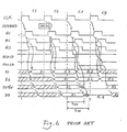
output circuit 17 is composed of an N-channel output transistor Tr1 which is connected between a power source and the output terminal DQ, the gate thereof being constituted by the conduction control signal D3T, and another N-channel output transistor Tr2 which is connected between the output terminal DQ and the ground, the gate thereof being constituted by the conduction control signal D3N. Theoutput circuit 17 is so designed that it outputs a high level of signal by actuating the output terminal DQ when only the conduction control signal D3T is activated, While it outputs a low level of signal by actuating the output terminal DQ when only the conduction control signal D3N is activated. On the other hand, when the conduction control signals D3T and D3N are being inactivated, the output terminal DQ is set into the state of high impedance. - Next, the operation of the conventional semiconductor memory device shown in FIG. 5 will be explained with reference also to FIG. 6 which shows a waveform diagram illustrating the operation in the case of a read burst operation with "CAS latency" being set to 3 (CAS latency= 3). This term "CAS latency", indicates that how many times of clock cycle is necessitated at a time interval, i.e. after the read command is input from the outside and before a data is output from the output terminal. Therefore, "CAS latency = 3" means that three cycles are necessitated. Meanwhile, the term "burst" indicates a continuous reading of data of any number of bits by the input of one read command. Therefore, at the
burst counter 4, an internal address corresponding to "burst length" is produced. - In response to the external clock CLK being shifted from a low level to a high level, the internal synchronizing signal 1 is changed to the high level, so that a high level of pulse is also generated in each of the internal synchronizing signals 2 and 3.
- When a mask command as command data DQM is input at the cycle C2, the mask signal MSK1B becomes level low in synchronism with the internal synchronizing signal 1 of this cycle. When the internal synchronism signal 3 is shifted from the low level to the high level, the mask signal MSK2B becomes low in level after a predetermined delay of the delay element DL. On the other hand, the data R2 corresponding to the cycle C2 is output at first as the data D1 from the
data amplifier 24 in synchronism with the internal synchronizing signal 2, and then as the data D2 from the D-F/F circuit 25 in synchronism with the internal synchronizing signal 3. - The data R2 is also transmitted in conformity with the data D2 to the conduction control signals D3T and D3N of the
output control circuit 14. However, when the mask signal MSK2B becomes low in level, the conduction control signals D3T and D3N becomes also low in level. As a result, both of N-channel output transistors Tr1 and TR2 in theoutput circuit 17 are turned OFF, thus rendering the output terminal DQ in a state of high impedance (Hi-Z). - Then, when no command is input at the cycle C3, the mask signal MSK1B becomes high in level in synchronism with the internal synchronizing signal 1 of this cycle. When the internal synchronizing signal 3 is shifted from a high level to a low level, the mask signal MSK2B becomes high in level after a predetermined delay of the delay element DL. Therefore, the data R3 is transmitted in conformity with the data D2 to the conduction control signals D3T and D3N of the output control circuit 14-16. As a result, one of N-channel output transistors Tr1 and and Tr2 is turned ON, and hence the data R3 is supplied to the output terminal DQ.
- The time interval starting from the state of high level of the external clock CLK at the
cycle 3 to the time when the output terminal DQ is turned into a state of high impedance (Hi-Z) is prescribed as a critical value called tHZ. Accordingly, the output terminal DQ is required to be turned into a state of high impedance (Hi-Z) earlier than the critical value tHZ. Moreover, the data R1 being supplied to the output terminal DQ after the external clock-CLK at the cycle C3 is turned into a high level is required to be retained for a time period longer than that prescribed by the critical value tOH. - According to this conventional semiconductor memory device, the timing for turning the output terminal DQ into a state of high impedance (Hi-Z) after the input of the mask command is determined by the delay time of the delay element DL for outputting the mask signal MSK2B, i.e. an output control signal. For this reason, if this delay time is too short, the output terminal DQ is turned into a state of high impedance (Hi-Z) too fast, thus badly affecting the critical value tOH. On the other hand, if this delay time is too long, the output terminal DQ is turned into a state of high impedance (Hi-Z) too late, thus badly affecting the critical value tHZ. Therefore, the optimization of the delay time of the delay element DL is very important.
- However, there is a problem in this optimization of the delay time that it requires an increase in the number of steps for designing it or a delay in the manufacture of the product, otherwise it requires a relaxation of the specified values tOH and tHZ.
- Another synchronous semiconductor memory device which is provided with a latch circuit for effecting a pipe-line operation is proposed in Japanese Laid-Open (Kokai) Patent Publication Hei 4-85792, or Japanese Laid-Open (Kokai) Patent Publication Hei 4-358392. However, these publications fail to disclose anything about the enable (data output) or disable (high impedance) of 5 output during the burst. For this reason the same problems as described above are raised in the control of output in the circuits disclosed in these patent publications.
- A semiconductor memory device corresponding to the preamble part of the main claim is known from EP-A-0 427 286.
- It is an object of the present invention to easily optimize the timing for the data output and high impedance of the output terminals in a synchronous semiconductor memory device having an internal pipe-line structure.
- This object is solved by the features of the main claim.
- Advantageous embodiments of the invention are mentioned in the sub-claims.
- The above and other objects, advantages and features of the present invention will be more apparent from the following description taken in conjunction with the accompanying drawings, in which:
- FIG. 1 is a block diagram showing one embodiment of the semiconductor memory device according to this invention;
- FIG. 2 is a waveform diagram showing an example of operation of the semiconductor memory device shown in FIG. 1;
- FIG. 3 is a block diagram showing another embodiment of the semiconductor memory device according to this invention;
- FIG. 4 is a waveform diagram showin an example of operation of the semiconductor memory device shown in FIG. 3;
- The FIG. 5 is a block diagram showin one example of the conventional semiconductor memory device; and
- FIG. 6 is a waveform diagram showing an example of operation of the semiconductor memory device shown in FIG. 5.
-
- Referring now to FIG. 1, there is shown a semiconductor memory device according to an embodiment of this invention, in which the same constituents as those shown in FIG. 5 are denoted by the same reference numerals to omit the further description thereof. In this memory, a data amplifier 11 receives the output from the
latch circuit 10 and producing a true data signal D1T and a complementary data signal D1N indicative of the received data. These signals D1T and D1N are supplied to anoutput control circuit 14 together with the mask signal MSK2B from D-F/F circuit 13 which responds to the change of the signal 3 from the high to low level. In response to these signals, theoutput control circuit 14 produces conduction control signals D2T and D2N which are in turn supplied to D-F/F circuits circuits output circuit 17 drives an output terminal DQ. - The
output control circuit 14 is composed of an AND gate AN1 supplied with the data signal D1T and the mask signal MSK2B and outputting the conduction control signal D2T, and an AND gate AN2 supplied with the data signal D1N and the mask signal MSK2B and outputting the conduction control signal D2N. The mask signal MSK2B to be input in this case is an output control signal for controlling whether the output terminal DQ of theoutput circuit 17 should be actuated or put into a high impedance. Theoutput control circuit 14 is designed to output a signal by activating one of the conduction control signals D2T and D2N or by inactivating each of the conduction control signals D2T and D2N in accordance with the mask signal MSK2B and the data signals D1T and D1N. - The
output circuit 17 is composed of an N-channel output transistor Tr1 connected between a power source and the output terminal DQ, the gate thereof being supplied with the conduction control signal D3T, and an N-channel output transistor Tr2 connected between the output terminal DQ and the ground, the gate thereof being supplied with the conduction control signal D3N. Theoutput circuit 17 is so designed that it outputs a high level of signal by actuating the output terminal DQ when the conduction control signal D3T is activated, i.e. the high level, while it outputs a low level of signal by actuating the output terminal DQ when the conduction control signal D3N is activated, i.e. the high level. On the other hand, when the conduction control signals D3T and D3N are both being inactivated, i.e., the low level, the output terminal DQ is brought into a state of high impedance. - Next, the operation of the above memory will be explained below with reference also to FIG. 2 which shows a waveform diagram illustrating a read burst operation when "CAS latency" is set to 3 3 (CAS latency = 3).
- When a mask command is input at the cycle C2, the mask signal MSK1B becomes low in level in synchronism with the internal synchronizing signsl 1 of this cycle. When the internal synchronizing signal 3 is shifted from a high level to a low level, the mask signal MSK2B becomes low in level. On the other hand, the data R2 corresponding to the cycle C2 is produced at first as the data D1T and D1N from the data amplifier 11 in synchronism with the internal synchronizing signal 2, and thereafter the conduction control signals D2T and D2N are produced from the
output control circuit 14. - However, since the mask signal MSK2B is at the low level-when the internal synchronizing signal 3 changes from the low level to the high level, the
output control circuit 14 changes each of the outputs D2T and D2N to the low level irrespective of the data R2. Accordingly, the output terminal DQ is not driven by the data R2, but brought into a state of high impedance (Hi-Z). - When no command is input at the cycle C3, on the other hand, the mask signal MSK1B becomes high in level in synchronism with the internal synchronizing signal 1 of this cycle. When the internal synchronizing signal 3 is shifted from a high level to a low level, the mask signal MSK2B becomes high. On the other hand, the data R3 complying with the
cycle 3 is output as the data D1T/N from the data amplifier 11 in synchronism with the internal synchronizing signal 2. However, the mask signal MSK2B becomes high in level by the change of the signal 3 from the high level to the low level. Accordingly, the conduction control signals D2T and D2N take the respective levels responsive to the data R3. These level are then latched by the F/F circuits - Turning to FIG. 3, there is shown a memory device according to another embodiment of this invention, in which the same constituents as those shown in FIG. 1 are denoted by the same reference numerals to omit the further description thereof. In this memory, there are provided an
input circuit 18 receiving a row address strobe signal RASB, an input circuit 19 receiving a column address strobe signal CASB, an input circuit 20 receiving a write-enable signal WEB, and an input circuit 21 receiving a chip-select signal CSB. These signals are then supplied to a command decoder 22 whose output signal is in turn applied to a latch circuit 23 controlled by the signal 1. The output of the latch circuit 23 is led out as a read signal READB and supplied to the F/F circuit 13. The output signal of the F/F circuit 13 is led out as an output-enable signal OEB in this embodiment, which is in turn supplied to theoutput control circuit 14. - Next, the operation of this memory device will be explained with reference also to FIG. 4 which shows a waveform diagram illustrating the operation wherein "CAS latency" is set to 3 (CAS latency = 3) and "burst length" is set to 2 (burst length = 2).
- When the signals RASB, CASB, WEB and CSB are supplied with a logic combination indicative of a read command at the cycle C1, this logic combination is decoded by the decoder 22. The read signal READB thereby becomes high in level in synchronism with the internal synchronizing signal 1 in the next cycle C2. When the internal synchronizing signal 3 is shifted from a high level to a low level, the output-enable signal OEB becomes high in level. However, the signal OEB is held at the low level at the timing when the signal 3 is changed to the high level. Accordingly, the data R1 does not appear at the output terminal DQ in the cycle C2.
- Since the signal OEB is changed to the high level at the end of the cycle C2, the control signal D2T and D2N take the respective levels responsive to the data R1 in the cycle C3. Accordingly, the high level of the internal synchronizing signal 3 in the cycle C3 has the F/
F circuits - Since the burst length is set to 2, the read signal READB becomes low in level in synchronization with the internal synchronizing signal 1 of the cycle C4, and when the internal synchronizing signal 3 is shifted from the high level to the low level in the cycle C4, the output-enable signal OEB is turned to the low level. Accordingly, the data R2 appears at the output terminal DQ in the cycle C4, but the output terminal DQ is brought into the high impedance state in the cycle C5.
- As explained above, the semiconductor memory device according to this invention is provided with a plurality of latching circuits, each adapted to individually latch and output a conduction control signal in synchronization with an internal synchronizing signal of controlling the internal pipe line, and each of the output transistors of the output circuit is separately controlled in accordance with the output of each of said latching circuits. Therefore, the non-uniformity in delay of time interval from the input of the internal synchronizing signal into each latching circuit to each output transistor can be minimized, so that all of the output terminals can be actuated with the same timing to take a high level or a low level, or to be put into the state of a high impedance. Accordingly, the optimization of the relevant specified timing values (tHZ, tOH) can be easily performed.
- Moreover, since the non-uniformity of delay can be minimized as explained above, the fluctuation due to non-uniformity in product and the changes in voltage of power source can be also minimized, so that the characteristic obtainable by the relevant specified timing values can be further improved.
- - It is apparent that the present invention is not limited to the above embodiments but may be changed and modified without departing from the scope and spirit of the invention. For example, by replacing the AND gate AN1 with a NAND gate, a P-channel MOS transistor can be employed in place of the transistor Tr1.
Claims (6)
- A semiconductor memory device comprising:characterized bya data output terminal (DQ),an output circuit (17) coupled to said output terminal and responding to first and second data signals (D2T, D3T, D2N, D3N) to drive said output terminal at a first logic level when said first and second data signals take a first state and at a second logic level when said first and second data signals take a second state and to bring said output terminal into a high impedance state when said first and second data signals take a third state,a first latch circuit (15) provided to latch and supply said first data signal (D2T,D3T) to said output circuit in response to a latch-enable signal (3), anda second latch circuit (16) provided to latch and supply said second data signal (D2N,D3N) to said output circuit in response to said latch-enable signal,
a third latch circuit (13) outputting a control signal (MSK2B) in response to an inverted signal of said latch-enable signals (3) so that said first and second data signals (D2T,D3T,D2N,D3N) take said third state in response to said control signal. - The device as claimed in claim 1, further comprising:a data amplifier (11) amplifying data stored in a selected memory cell (6) to output a third data signal (D1T) and a fourth data signal (D1N) complementary to said third data signal; and an output control circuit (14) comprising a first logic gate (AN1) responding said third data signal (D1T) and said control signal (MSK2B) to output said first data signal (D2T) and a second logic gate (AN2) responding said fourth data signal (D1N) and said control signal (MSK2B) to output said second data signal (D2N).
- The device as claimed in claim 1, further comprising:an output control circuit (14), connected to said first latch (15) circuit and to said second latch circuit (16), outputting said first and second data signals (D2T, D2N) in response to a third data signal (D1T) and a fourth data signal (D1N), respectively, said output control circuit (14) further receiving said control signal (MSK2B) controlling said first and second data signals (D2T,D2N) to take said third state irrespective of a level of said third and fourth data signals (D1T,D1N) when said control signal is at a predetermined level.
- The device as claimed in claim 3, further comprising:a command decoder (22) receiving and decoding a plurality of command signals (RASB,CASB,WEB,CSB) to produce a decoded command signal (READB); anda fourth latch circuit (LATCH) latching and supplying said decoded command signal (READB) to said third latch circuit (13) as said control signal in response to a clock signal (CLK).
- The device as claimed in claim 3, further comprising:a data amplifier (11) amplifying said data stored in said selected memory cell (6) to output said third data signal (D1) and said fourth data signal (D1N) complementary to said third data signal (D1T); wherein said output control circuit (14) comprises a first logic gate (AN1) responding said third data signal (D1T) and said control signal (OEB) to output said first data signal (D2T) and a second logic gate (AN2) responding said fourth data signal (D1N) and said control signal (OEB) to output said second data signal.
- The device as claimed in claim 2 or 5, wherein each of said first through third latch circuits is a D-Flip/Flop and each of said first and second logic gates is an AND gate (AN1, AN2).
Applications Claiming Priority (3)
| Application Number | Priority Date | Filing Date | Title |
|---|---|---|---|
| JP01407496A JP3192077B2 (en) | 1996-01-30 | 1996-01-30 | Semiconductor storage device |
| JP1407496 | 1996-01-30 | ||
| JP14074/96 | 1996-01-30 |
Publications (3)
| Publication Number | Publication Date |
|---|---|
| EP0788108A2 EP0788108A2 (en) | 1997-08-06 |
| EP0788108A3 EP0788108A3 (en) | 1999-08-18 |
| EP0788108B1 true EP0788108B1 (en) | 2003-08-27 |
Family
ID=11850968
Family Applications (1)
| Application Number | Title | Priority Date | Filing Date |
|---|---|---|---|
| EP97101364A Expired - Lifetime EP0788108B1 (en) | 1996-01-30 | 1997-01-29 | Synchronous semi-conductor memory device |
Country Status (5)
| Country | Link |
|---|---|
| US (1) | US5822254A (en) |
| EP (1) | EP0788108B1 (en) |
| JP (1) | JP3192077B2 (en) |
| KR (1) | KR100260071B1 (en) |
| DE (1) | DE69724302T2 (en) |
Families Citing this family (11)
| Publication number | Priority date | Publication date | Assignee | Title |
|---|---|---|---|---|
| JP3922765B2 (en) * | 1997-07-22 | 2007-05-30 | 富士通株式会社 | Semiconductor device system and semiconductor device |
| JP3244035B2 (en) * | 1997-08-15 | 2002-01-07 | 日本電気株式会社 | Semiconductor storage device |
| JP3716080B2 (en) * | 1997-08-28 | 2005-11-16 | エルピーダメモリ株式会社 | Output circuit of semiconductor memory device |
| JPH11162174A (en) * | 1997-11-25 | 1999-06-18 | Mitsubishi Electric Corp | Synchronous semiconductor memory device |
| KR100252054B1 (en) * | 1997-12-04 | 2000-04-15 | 윤종용 | Synchronous semiconductor memory device having wave pipelining control scheme and data output method |
| US6122203A (en) * | 1998-06-29 | 2000-09-19 | Cypress Semiconductor Corp. | Method, architecture and circuit for writing to and reading from a memory during a single cycle |
| US5986970A (en) * | 1998-06-29 | 1999-11-16 | Cypress Semiconductor Corp. | Method, architecture and circuit for writing to a memory |
| US6301188B1 (en) * | 1999-08-11 | 2001-10-09 | Micron Technology, Inc. | Method and apparatus for registering free flow information |
| JP4607444B2 (en) * | 2002-11-18 | 2011-01-05 | 三星電子株式会社 | Semiconductor device, data retrieval circuit, memory cell array interpretation method, and data retrieval method |
| JP4104634B2 (en) * | 2006-05-23 | 2008-06-18 | シャープ株式会社 | Semiconductor device |
| JP5876271B2 (en) | 2011-11-01 | 2016-03-02 | ルネサスエレクトロニクス株式会社 | Memory control device |
Family Cites Families (13)
| Publication number | Priority date | Publication date | Assignee | Title |
|---|---|---|---|---|
| JPS61148692A (en) * | 1984-12-24 | 1986-07-07 | Nippon Telegr & Teleph Corp <Ntt> | Memory device |
| JPH02137189A (en) * | 1988-11-17 | 1990-05-25 | Hitachi Ltd | Memory circuits and digital devices |
| JPH0344890A (en) * | 1989-07-12 | 1991-02-26 | Toshiba Corp | Data output control circuit for semiconductor memory |
| JP2534782B2 (en) * | 1989-11-10 | 1996-09-18 | 株式会社東芝 | Semiconductor device |
| JP2573392B2 (en) * | 1990-03-30 | 1997-01-22 | 株式会社東芝 | Semiconductor storage device |
| JPH0485792A (en) | 1990-07-27 | 1992-03-18 | Toshiba Corp | Semiconductor storage |
| JP3178859B2 (en) | 1991-06-05 | 2001-06-25 | 株式会社東芝 | Random access memory device and pipeline / page mode control method thereof |
| JP2830594B2 (en) * | 1992-03-26 | 1998-12-02 | 日本電気株式会社 | Semiconductor memory device |
| JPH06202933A (en) * | 1992-12-28 | 1994-07-22 | Toshiba Corp | Synchronous large-scale integrated circuit memory device |
| JPH07192470A (en) * | 1993-03-08 | 1995-07-28 | Nec Ic Microcomput Syst Ltd | Output circuit for semiconductor memory |
| US5488581A (en) * | 1993-10-28 | 1996-01-30 | Fujitsu Limited | Semiconductor memory device |
| JP3013714B2 (en) | 1994-09-28 | 2000-02-28 | 日本電気株式会社 | Semiconductor storage device |
| US5666071A (en) * | 1995-12-01 | 1997-09-09 | Advanced Micro Devices, Inc. | Device and method for programming high impedance states upon select input/output pads |
-
1996
- 1996-01-30 JP JP01407496A patent/JP3192077B2/en not_active Expired - Fee Related
-
1997
- 1997-01-29 DE DE69724302T patent/DE69724302T2/en not_active Expired - Lifetime
- 1997-01-29 US US08/791,034 patent/US5822254A/en not_active Expired - Lifetime
- 1997-01-29 EP EP97101364A patent/EP0788108B1/en not_active Expired - Lifetime
- 1997-01-30 KR KR1019970002807A patent/KR100260071B1/en not_active Expired - Fee Related
Also Published As
| Publication number | Publication date |
|---|---|
| DE69724302T2 (en) | 2004-06-03 |
| US5822254A (en) | 1998-10-13 |
| EP0788108A2 (en) | 1997-08-06 |
| EP0788108A3 (en) | 1999-08-18 |
| JPH09204768A (en) | 1997-08-05 |
| KR100260071B1 (en) | 2000-07-01 |
| KR970060222A (en) | 1997-08-12 |
| DE69724302D1 (en) | 2003-10-02 |
| JP3192077B2 (en) | 2001-07-23 |
Similar Documents
| Publication | Publication Date | Title |
|---|---|---|
| KR100500921B1 (en) | Semiconductor memory device with ability to mediate impedance of data output-driver | |
| US6385127B1 (en) | Synchronous semiconductor device and method for latching input signals | |
| CN100568386C (en) | Semiconductor memory device capable of adjusting impedance of data output driver | |
| US7558127B2 (en) | Data output circuit and method in DDR synchronous semiconductor device | |
| US6260128B1 (en) | Semiconductor memory device which operates in synchronism with a clock signal | |
| US6522600B2 (en) | Fast cycle RAM and data readout method therefor | |
| US6198674B1 (en) | Data strobe signal generator of semiconductor device using toggled pull-up and pull-down signals | |
| US5822254A (en) | Synchronous semiconductor memory device | |
| JPH09139084A (en) | Semiconductor memory | |
| US6636443B2 (en) | Semiconductor memory device having row buffers | |
| US6073219A (en) | Semiconductor memory device with high speed read-modify-write function | |
| US6987699B2 (en) | Clock driver in semiconductor memory device | |
| KR100507855B1 (en) | A QFCB siganl generator for read operation in DDR SDRAM | |
| US6671788B2 (en) | Synchronous semiconductor memory device having a burst mode for improving efficiency of using the data bus | |
| US5732042A (en) | Dram array with local latches | |
| KR100650845B1 (en) | A buffer control circuit for reducing power consumption, a semiconductor memory device for a memory module including the same, and a control operation method thereof | |
| KR19990047472A (en) | Synchronous semiconductor memory device having wave pipelining control structure and data output method | |
| JP3317243B2 (en) | Semiconductor storage device | |
| US6930950B2 (en) | Semiconductor memory device having self-precharge function | |
| KR100296919B1 (en) | Data strobe signal output buffers in memory device | |
| JPH11297072A (en) | Semiconductor memory system and its control method | |
| KR100191022B1 (en) | Semiconductor integrated circuit device | |
| US5914899A (en) | Semiconductor memory having a page mode in which previous data in an output circuit is reset before new data is supplied | |
| KR20010087643A (en) | Data input buffer circuit | |
| JP3528964B2 (en) | Semiconductor device |
Legal Events
| Date | Code | Title | Description |
|---|---|---|---|
| PUAI | Public reference made under article 153(3) epc to a published international application that has entered the european phase |
Free format text: ORIGINAL CODE: 0009012 |
|
| AK | Designated contracting states |
Kind code of ref document: A2 Designated state(s): DE FR GB |
|
| PUAL | Search report despatched |
Free format text: ORIGINAL CODE: 0009013 |
|
| AK | Designated contracting states |
Kind code of ref document: A3 Designated state(s): DE FR GB |
|
| 17P | Request for examination filed |
Effective date: 19990709 |
|
| 17Q | First examination report despatched |
Effective date: 20020121 |
|
| GRAH | Despatch of communication of intention to grant a patent |
Free format text: ORIGINAL CODE: EPIDOS IGRA |
|
| RAP1 | Party data changed (applicant data changed or rights of an application transferred) |
Owner name: NEC ELECTRONICS CORPORATION Owner name: NEC CORPORATION |
|
| GRAS | Grant fee paid |
Free format text: ORIGINAL CODE: EPIDOSNIGR3 |
|
| GRAA | (expected) grant |
Free format text: ORIGINAL CODE: 0009210 |
|
| AK | Designated contracting states |
Designated state(s): DE FR GB |
|
| REG | Reference to a national code |
Ref country code: GB Ref legal event code: FG4D |
|
| REF | Corresponds to: |
Ref document number: 69724302 Country of ref document: DE Date of ref document: 20031002 Kind code of ref document: P |
|
| ET | Fr: translation filed | ||
| PLBE | No opposition filed within time limit |
Free format text: ORIGINAL CODE: 0009261 |
|
| STAA | Information on the status of an ep patent application or granted ep patent |
Free format text: STATUS: NO OPPOSITION FILED WITHIN TIME LIMIT |
|
| 26N | No opposition filed |
Effective date: 20040528 |
|
| REG | Reference to a national code |
Ref country code: GB Ref legal event code: 732E |
|
| REG | Reference to a national code |
Ref country code: FR Ref legal event code: TP |
|
| REG | Reference to a national code |
Ref country code: FR Ref legal event code: CD |
|
| REG | Reference to a national code |
Ref country code: DE Ref legal event code: R082 Ref document number: 69724302 Country of ref document: DE Representative=s name: GLAWE DELFS MOLL - PARTNERSCHAFT VON PATENT- U, DE |
|
| REG | Reference to a national code |
Ref country code: DE Ref legal event code: R082 Ref document number: 69724302 Country of ref document: DE Representative=s name: GLAWE DELFS MOLL PARTNERSCHAFT MBB VON PATENT-, DE Effective date: 20120828 Ref country code: DE Ref legal event code: R082 Ref document number: 69724302 Country of ref document: DE Representative=s name: GLAWE DELFS MOLL - PARTNERSCHAFT VON PATENT- U, DE Effective date: 20120828 Ref country code: DE Ref legal event code: R081 Ref document number: 69724302 Country of ref document: DE Owner name: RENESAS ELECTRONICS CORPORATION, KAWASAKI-SHI, JP Free format text: FORMER OWNER: NEC ELECTRONICS CORP., KAWASAKI, KANAGAWA, JP Effective date: 20120828 Ref country code: DE Ref legal event code: R081 Ref document number: 69724302 Country of ref document: DE Owner name: RENESAS ELECTRONICS CORPORATION, JP Free format text: FORMER OWNER: NEC ELECTRONICS CORP., KAWASAKI, JP Effective date: 20120828 |
|
| PGFP | Annual fee paid to national office [announced via postgrant information from national office to epo] |
Ref country code: FR Payment date: 20130204 Year of fee payment: 17 Ref country code: DE Payment date: 20130123 Year of fee payment: 17 Ref country code: GB Payment date: 20130123 Year of fee payment: 17 |
|
| REG | Reference to a national code |
Ref country code: DE Ref legal event code: R119 Ref document number: 69724302 Country of ref document: DE |
|
| GBPC | Gb: european patent ceased through non-payment of renewal fee |
Effective date: 20140129 |
|
| REG | Reference to a national code |
Ref country code: DE Ref legal event code: R119 Ref document number: 69724302 Country of ref document: DE Effective date: 20140801 |
|
| PG25 | Lapsed in a contracting state [announced via postgrant information from national office to epo] |
Ref country code: DE Free format text: LAPSE BECAUSE OF NON-PAYMENT OF DUE FEES Effective date: 20140801 |
|
| REG | Reference to a national code |
Ref country code: FR Ref legal event code: ST Effective date: 20140930 |
|
| PG25 | Lapsed in a contracting state [announced via postgrant information from national office to epo] |
Ref country code: GB Free format text: LAPSE BECAUSE OF NON-PAYMENT OF DUE FEES Effective date: 20140129 Ref country code: FR Free format text: LAPSE BECAUSE OF NON-PAYMENT OF DUE FEES Effective date: 20140131 |