EP0786865A2 - A precision oscillator circuit - Google Patents
A precision oscillator circuit Download PDFInfo
- Publication number
- EP0786865A2 EP0786865A2 EP97300509A EP97300509A EP0786865A2 EP 0786865 A2 EP0786865 A2 EP 0786865A2 EP 97300509 A EP97300509 A EP 97300509A EP 97300509 A EP97300509 A EP 97300509A EP 0786865 A2 EP0786865 A2 EP 0786865A2
- Authority
- EP
- European Patent Office
- Prior art keywords
- coupled
- output
- transistor
- input
- voltage
- Prior art date
- Legal status (The legal status is an assumption and is not a legal conclusion. Google has not performed a legal analysis and makes no representation as to the accuracy of the status listed.)
- Withdrawn
Links
Images

Classifications
-
- G—PHYSICS
- G01—MEASURING; TESTING
- G01P—MEASURING LINEAR OR ANGULAR SPEED, ACCELERATION, DECELERATION, OR SHOCK; INDICATING PRESENCE, ABSENCE, OR DIRECTION, OF MOVEMENT
- G01P3/00—Measuring linear or angular speed; Measuring differences of linear or angular speeds
- G01P3/42—Devices characterised by the use of electric or magnetic means
- G01P3/44—Devices characterised by the use of electric or magnetic means for measuring angular speed
- G01P3/48—Devices characterised by the use of electric or magnetic means for measuring angular speed by measuring frequency of generated current or voltage
-
- G—PHYSICS
- G01—MEASURING; TESTING
- G01P—MEASURING LINEAR OR ANGULAR SPEED, ACCELERATION, DECELERATION, OR SHOCK; INDICATING PRESENCE, ABSENCE, OR DIRECTION, OF MOVEMENT
- G01P1/00—Details of instruments
- G01P1/07—Indicating devices, e.g. for remote indication
-
- H—ELECTRICITY
- H03—ELECTRONIC CIRCUITRY
- H03K—PULSE TECHNIQUE
- H03K3/00—Circuits for generating electric pulses; Monostable, bistable or multistable circuits
- H03K3/01—Details
- H03K3/011—Modifications of generator to compensate for variations in physical values, e.g. voltage, temperature
-
- H—ELECTRICITY
- H03—ELECTRONIC CIRCUITRY
- H03K—PULSE TECHNIQUE
- H03K3/00—Circuits for generating electric pulses; Monostable, bistable or multistable circuits
- H03K3/01—Details
- H03K3/017—Adjustment of width or dutycycle of pulses
-
- H—ELECTRICITY
- H03—ELECTRONIC CIRCUITRY
- H03K—PULSE TECHNIQUE
- H03K3/00—Circuits for generating electric pulses; Monostable, bistable or multistable circuits
- H03K3/02—Generators characterised by the type of circuit or by the means used for producing pulses
- H03K3/023—Generators characterised by the type of circuit or by the means used for producing pulses by the use of differential amplifiers or comparators, with internal or external positive feedback
- H03K3/0231—Astable circuits
Definitions
- This invention relates to electronic oscillator circuits used to generate digital clock signals and more specifically to precision oscillator circuits. 2.
- Precision clock signals are widely used in digital circuits to synchronize the activities of one digital circuit to the rest of the circuits in the system.
- a digital system may include one or more microprocessors, buss controllers, peripheral controllers, memory, and peripherals such as disk drives, all of which would be synchronized from one system clock.
- a less complex system may include a single microcontroller with at least one input device, such as a sensor, and at least one output device, such as an ignition controller.
- a less complex system may include an oscillator to provide a frequency reference for the speedometer or tachometer of an automobile. It will be appreciated that precision oscillators are used in simple systems, complex systems, and everything in between.
- the oscillation cycle begins by setting and resetting RS flip-flop 20.
- the flip-flop 20 is set by current source 2 charging capacitor 4.
- the voltage on the non-inverting input of comparator 8 rises.
- Vcalib the voltage on the inverting input
- the output of comparator 8 will rise to the positive voltage rail of the comparator thereby setting the output of flip-flop 20 to a digital "1" voltage.
- This subsequently turns off current source 2, turns on transistor 6, turns off transistor 14 (which was on), and turns on current source 10. Consequently, capacitor 12 is charged by current source 10 and the voltage on the non-inverted input of comparator 16 rises.
- this circuit requires two capacitors 4 and 12, two comparators 8 and 16, and an RS flip-flop.
- the invention can be summarized as a precision oscillator constructed from a reference current generator, a charge control stage, a capacitor, a comparator, and a voltage threshold generator.
- the reference current generator generates a reference current which is used by the charge control stage to either charge or discharge the capacitor.
- the comparator compares the voltage on the capacitor to one of two voltages from the voltage threshold generator.
- the frequency of oscillation is controlled by an external resistor and an external capacitor. Alternatively, the frequency of oscillation can be controlled by adding or subtracting parallel transistors in a current mirror in the reference current generator.
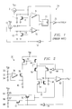
- Fig. 1 is a schematic drawing of a precision oscillator as known in the prior art.
- Fig. 2 is a schematic drawing of a precision oscillator as disclosed in an embodiment of the invention.
- Fig. 3 is a schematic drawing of a current source as described in an alternate embodiment of the invention.
- Fig. 4 is a timing diagram of the disclosed invention.
- Fig. 5 is block diagram of speedometer system which includes the disclosed invention.
- Precision oscillator 30 is constructed with a reference current generator, a charge control stage, a capacitor, a comparator, and a voltage threshold generator.
- the reference current generator is constructed using resistors 32, 34, and 40, amplifier 36, N-channel transistor 38, and P-channel transistors 42 and 44. More specifically, the first end of resistor 32 is connected to a voltage source Vdd and the second end of resistor 32 is connected to the noninverting input of amplifier 36 and the first end of resistor 34. The second end of resistor 34 is connected to ground.
- the output of amplifier 36 is connected to the gate of transistor 38.
- the source of transistor 38 is connected to the inverting input of amplifier 36 and to the first end of resistor 40, the second end of resistor 40 is connected to ground.
- transistor 38 will be driven by amplifier 36 so that the voltage on resistor 40 follows the voltage on noninverting input of comparator 36.
- the drain of transistor 38 is connected to a current mirror made from transistors 42 and 44.
- the drain of transistor 38 is connected to the drain and gate of transistor 42 and the gate of transistor 44.
- the sources of transistors 42 and 44 are connected to Vdd.
- the drain of transistor 44 is the mirrored current output of the current mirror and is also the output of the reference current generator.
- the charge control stage is constructed using P-channel transistors 50 and 52, N-channel transistors 54 and 56, and inverter 60.
- the sources of transistors 50 and 52 are coupled together to form the input of the charge control stage and are therefore, coupled to the output of the reference current generator.
- the gate of transistor 50 is connected to the input of inverter 60.
- the output of inverter 60 is connected to the gate of transistor 52.
- the drain of transistor 50 is connected to the drain and gate of transistor 54 and to the gate of transistor 56.
- the sources of transistors 54 and 56 are connected to ground.
- the drains of transistors 52 and 56 are connected together to form the output of the charge control stage. This output is connected to a first end of capacitor 58 and the inverting input of comparator 62.
- the noninverting input of comparator 62 is connected to the output of the voltage threshold generator.
- the output of the comparator is the output of the oscillator and is connected to the input of inverter 60, the gate of transistor 50, and the gates of transistors 70 and 72.
- the voltage threshold generator is constructed by connecting three resistors 64, 66 and 68 in series across the supply voltage. These three resistors can be of equal value such that node 65 between resistor 64 and 66 has a voltage of approximately 2/3 the supply voltage. Similarly, the voltage at node 67 between resistors 66 and 68 has a voltage of approximately 1/3 the supply voltage. Alternate methods for generating two reference voltages will be known by persons skilled in the art.
- the source of transistor 70 is connected to node 65.
- the source of transistor 72 is connected to node 67.
- the gates of transistors 70 and 72 are connected to the output of inverter 74.
- the input of inverter is connected to the output of comparator 62.
- the drain of transistor 70 and the source of transistor 72 are connected together and to the noninverting input of comparator 62.
- the charge control stage is used to direct the reference current generated from the reference current generator either to capacitor 58 or to remove the reference current from the capacitor. More specifically, when the output of comparator 62 is high, transistor 50 is turned off and transistor 52 is turned on. Therefore, the reference current from the reference current generator is conducted through transistor 52 onto capacitor 58. Conversely, when the output of comparator 62 is low, transistor 50 is on and transistor 52 is turned off. Therefore, the reference current from the reference current generator is conducted through transistor 50 and therefore, through the current mirror made from transistors 54 and 56. If the ratio between transistors 54 and 56 is approximately equal to one, a current approximately equal to the reference current will be discharged from capacitor 58. In short, the charge control stage either charges capacitor 58 or discharges capacitor 58 responsive to the output of comparator 62.
- the voltage threshold generator couples either the voltage at node 65 or the voltage at node 67 to the noninverting input of comparator 62.
- the output of comparator 62 is high, the output of the inverter 74 is low so that transistor 70 is on and transistor 72 is turned off so that the voltage at node 65 is coupled to the noninverting input of comparator 62.
- the voltage at node 67 is coupled to the noninverting input of comparator 62 when the output of comparator 62 is at a low voltage level which drives the output of inverter 74 high.
- an oscillation cycle at begins To when the output of comparator 62, Vo is at a low voltage level.
- the charge control stage is discharging capacitor 58 at a rate proportional to the reference current and inversely proportional to the size of the capacitor.
- the voltage on the capacitor, Vc is discharging at a constant rate.
- the noninverting input of comparator 62 is coupled to the voltage, V 67 at node 67.
- the comparator 62 switches to a high voltage state, as shown at T 1 . Consequently, the charge control stage begins to charge capacitor 58 and the voltage threshold generator changes the voltage threshold to the voltage at node 65.
- comparator 62 When the voltage on capacitor 58 exceeds the voltage on node 65 comparator 62 will again change states such that the output is now again at a low voltage and the oscillation cycle will restart, as shown at T 2 .
- the frequency of oscillation is controlled by controlling reference current and the capacitance of C58.
- FIG 2 shows transistor 44 as the mirrored current stage of a current mirror in the reference current generator.
- Figure 3 shows that transistor 44 of figure 2 can be a series of transistors coupled in parallel. More specifically, figure 3 shows the source of transistors 44', 44",44'", 44"", and 44 n all connect to the source voltage Vdd. Similarly, the drains of transistors 44', 44", 44"', 44"", and 44 n are all connected together and form the output of the current mirror. The gate of transistor 44' would be connected to the gate and drain of transistor 42 of figure 2.
- the gate of transistors 44' through 44 n can either be connect to Vdd or to the gate of transistor 44'.
- this circuit also provides the benefit of providing a precision oscillator which oscillates as a function of current (the reference current) instead of as a function of the supply voltage.
- FIG. 5 illustrates a speedometer system 80 which uses the precision oscillator 30. More specifically, this figure shows a wheel sensor 82 coupled to an analog voltage converter 84. The analog voltage converter 84 and precision oscillator are combined to drive the air core gauge motor 86, which drives the speedometer display as is known in the art.
Landscapes
- Physics & Mathematics (AREA)
- General Physics & Mathematics (AREA)
- Electronic Switches (AREA)
- Stabilization Of Oscillater, Synchronisation, Frequency Synthesizers (AREA)
- Inductance-Capacitance Distribution Constants And Capacitance-Resistance Oscillators (AREA)
Abstract
Description
- This invention relates to electronic oscillator circuits used to generate digital clock signals and more specifically to precision oscillator circuits.
2. - The problem addressed by this invention is encountered in oscillator circuits used for generating precision clock signals. Precision clock signals are widely used in digital circuits to synchronize the activities of one digital circuit to the rest of the circuits in the system. A digital system may include one or more microprocessors, buss controllers, peripheral controllers, memory, and peripherals such as disk drives, all of which would be synchronized from one system clock. A less complex system may include a single microcontroller with at least one input device, such as a sensor, and at least one output device, such as an ignition controller. And yet a less complex system may include an oscillator to provide a frequency reference for the speedometer or tachometer of an automobile. It will be appreciated that precision oscillators are used in simple systems, complex systems, and everything in between.
- Reference now to figure 1, a
precision oscillator 24 according to the prior art is shown. The oscillation cycle begins by setting and resetting RS flip-flop 20. The flip-flop 20 is set bycurrent source 2charging capacitor 4. Ascapacitor 4 is charged, the voltage on the non-inverting input ofcomparator 8 rises. When this voltage exceeds the voltage, Vcalib, on the inverting input, the output ofcomparator 8 will rise to the positive voltage rail of the comparator thereby setting the output of flip-flop 20 to a digital "1" voltage. This subsequently turns offcurrent source 2, turns ontransistor 6, turns off transistor 14 (which was on), and turns oncurrent source 10. Consequently,capacitor 12 is charged bycurrent source 10 and the voltage on the non-inverted input ofcomparator 16 rises. When the voltage on the non-inverting input ofcomparator 16 exceeds the voltage on the inverting input, the output ofcomparator 16 will swing to a the positive voltage rail thereby resetting the output of flip-flop 20 to a digital "0". The resetting of flip-flop 20 subsequently turnscurrent source 2 on,transistor 6 off,transistor 14 on, andcurrent source 10 off, thereby restarting the oscillation cycle. - From figure 1, it is shown that this circuit requires two
capacitors comparators - Therefore, it is an object of the invention to provide a precision oscillator which requires fewer capacitors.
- It is yet another object of the invention to require one comparator instead of two comparators.
- It is and yet another object of the invention to provide a precision oscillator which oscillates at a frequency independent of the of the supply voltage.
- These and other objects, features, and advantages of the invention will be apparent to those skilled in the art from the following detailed description of the invention, when read with the drawings and appended claims.
- The invention can be summarized as a precision oscillator constructed from a reference current generator, a charge control stage, a capacitor, a comparator, and a voltage threshold generator. The reference current generator generates a reference current which is used by the charge control stage to either charge or discharge the capacitor. The comparator compares the voltage on the capacitor to one of two voltages from the voltage threshold generator. The frequency of oscillation is controlled by an external resistor and an external capacitor. Alternatively, the frequency of oscillation can be controlled by adding or subtracting parallel transistors in a current mirror in the reference current generator.
- Some embodiments of the invention will now be described by way of example and with reference to the accompanying drawings in which:
- Fig. 1 is a schematic drawing of a precision oscillator as known in the prior art.
- Fig. 2 is a schematic drawing of a precision oscillator as disclosed in an embodiment of the invention.
- Fig. 3 is a schematic drawing of a current source as described in an alternate embodiment of the invention.
- Fig. 4 is a timing diagram of the disclosed invention.
- Fig. 5 is block diagram of speedometer system which includes the disclosed invention.
- A precision oscillator constructed according to a the preferred embodiment of the invention will be described.
-
Precision oscillator 30 is constructed with a reference current generator, a charge control stage, a capacitor, a comparator, and a voltage threshold generator. - The reference current generator is constructed using
resistors amplifier 36, N-channel transistor 38, and P-channel transistors resistor 32 is connected to a voltage source Vdd and the second end ofresistor 32 is connected to the noninverting input ofamplifier 36 and the first end ofresistor 34. The second end ofresistor 34 is connected to ground. The output ofamplifier 36 is connected to the gate oftransistor 38. The source oftransistor 38 is connected to the inverting input ofamplifier 36 and to the first end ofresistor 40, the second end ofresistor 40 is connected to ground. This configuration is commonly referred to as a voltage follower sincetransistor 38 will be driven byamplifier 36 so that the voltage onresistor 40 follows the voltage on noninverting input ofcomparator 36. The drain oftransistor 38 is connected to a current mirror made fromtransistors transistor 38 is connected to the drain and gate oftransistor 42 and the gate oftransistor 44. The sources oftransistors transistor 44 is the mirrored current output of the current mirror and is also the output of the reference current generator. - The charge control stage is constructed using P-
channel transistors channel transistors transistors transistor 50 is connected to the input ofinverter 60. The output ofinverter 60 is connected to the gate oftransistor 52. The drain oftransistor 50 is connected to the drain and gate oftransistor 54 and to the gate oftransistor 56. The sources oftransistors transistors capacitor 58 and the inverting input ofcomparator 62. - The noninverting input of
comparator 62 is connected to the output of the voltage threshold generator. The output of the comparator is the output of the oscillator and is connected to the input ofinverter 60, the gate oftransistor 50, and the gates oftransistors - The voltage threshold generator is constructed by connecting three
resistors 64, 66 and 68 in series across the supply voltage. These three resistors can be of equal value such that node 65 between resistor 64 and 66 has a voltage of approximately 2/3 the supply voltage. Similarly, the voltage at node 67 betweenresistors 66 and 68 has a voltage of approximately 1/3 the supply voltage. Alternate methods for generating two reference voltages will be known by persons skilled in the art. The source oftransistor 70 is connected to node 65. The source oftransistor 72 is connected to node 67. The gates oftransistors inverter 74. The input of inverter is connected to the output ofcomparator 62. The drain oftransistor 70 and the source oftransistor 72 are connected together and to the noninverting input ofcomparator 62. - In operation, the reference current generator generates a reference current which is equal a function of the voltage at
node 33, the resistance ofresistor 40, and the ratio oftransistors amplifier 36 is configured as a voltage follow, the voltage on the noninverting input ofamplifier 36 will be maintained acrossresistor 40. Thus, the current throughresistor 40 is:
resistors transistors transistor 44 and can be adjusted by adjusting variables in the above equation as well as the ratio of area betweentransistors - The charge control stage is used to direct the reference current generated from the reference current generator either to
capacitor 58 or to remove the reference current from the capacitor. More specifically, when the output ofcomparator 62 is high,transistor 50 is turned off andtransistor 52 is turned on. Therefore, the reference current from the reference current generator is conducted throughtransistor 52 ontocapacitor 58. Conversely, when the output ofcomparator 62 is low,transistor 50 is on andtransistor 52 is turned off. Therefore, the reference current from the reference current generator is conducted throughtransistor 50 and therefore, through the current mirror made fromtransistors transistors capacitor 58. In short, the charge control stage either charges capacitor 58 ordischarges capacitor 58 responsive to the output ofcomparator 62. - The voltage threshold generator couples either the voltage at node 65 or the voltage at node 67 to the noninverting input of
comparator 62. When the output ofcomparator 62 is high, the output of theinverter 74 is low so thattransistor 70 is on andtransistor 72 is turned off so that the voltage at node 65 is coupled to the noninverting input ofcomparator 62. Conversely, the voltage at node 67 is coupled to the noninverting input ofcomparator 62 when the output ofcomparator 62 is at a low voltage level which drives the output ofinverter 74 high. - As shown in figure 4, an oscillation cycle at begins To when the output of
comparator 62, Vo is at a low voltage level. In this state, the charge control stage is dischargingcapacitor 58 at a rate proportional to the reference current and inversely proportional to the size of the capacitor. The voltage on the capacitor, Vc, is discharging at a constant rate. The noninverting input ofcomparator 62 is coupled to the voltage, V67 at node 67. When the voltage oncapacitor 58 falls below the voltage on the noninverting input ofcomparator 62 thecomparator 62 switches to a high voltage state, as shown at T1. Consequently, the charge control stage begins to chargecapacitor 58 and the voltage threshold generator changes the voltage threshold to the voltage at node 65. When the voltage oncapacitor 58 exceeds the voltage on node 65comparator 62 will again change states such that the output is now again at a low voltage and the oscillation cycle will restart, as shown at T2. The frequency of oscillation is controlled by controlling reference current and the capacitance of C58. - By using the disclosed precision oscillator only one
capacitor 58 is required, as compared to two capacitors in the prior art. Additionally, only onecomparator 62 is required, compared to the two comparators required in the prior art. Figure 2 showstransistor 44 as the mirrored current stage of a current mirror in the reference current generator. Figure 3 shows thattransistor 44 of figure 2 can be a series of transistors coupled in parallel. More specifically, figure 3 shows the source oftransistors 44', 44",44'", 44"", and 44n all connect to the source voltage Vdd. Similarly, the drains oftransistors 44', 44", 44"', 44"", and 44n are all connected together and form the output of the current mirror. The gate of transistor 44' would be connected to the gate and drain oftransistor 42 of figure 2. Additionally, the gate of transistors 44' through 44n can either be connect to Vdd or to the gate of transistor 44'. Thus, it would be possible to trim the current of the reference current generator in either the manufacturing process or the design process of the precision oscillator. Consequently, this circuit also provides the benefit of providing a precision oscillator which oscillates as a function of current (the reference current) instead of as a function of the supply voltage. - Figure 5 illustrates a
speedometer system 80 which uses theprecision oscillator 30. More specifically, this figure shows awheel sensor 82 coupled to ananalog voltage converter 84. Theanalog voltage converter 84 and precision oscillator are combined to drive the aircore gauge motor 86, which drives the speedometer display as is known in the art. - Although the invention has been described and illustrated with a certain degree of particularity, it is understood that the present disclosure has been made only by way of example, and that numerous changes in the combination and arrangement of parts can be resorted to by those skilled in the art without departing from the spirit and scope of the invention, as hereinafter claimed.
Claims (14)
- A precision oscillator circuit comprising:a reference current generator having an output for supplying a reference current;a charge control stage having a first input coupled to the output of the reference current generator, having a second input, and having an output;a capacitor having a first plate coupled to the output of the charge control stage and having a second plate coupled to ground;a comparator having a first input coupled to the first plate of the capacitor, having a second input, and having an output coupled to the second input of the charge control stage; anda voltage threshold generator having an input coupled to the output of the comparator and having an output coupled to the second input of the comparator.
- The precision oscillator of claim 1 wherein the charge control stage comprises:an inverter having an input coupled to the output of the comparator and having an output;a first transistor having a control element coupled to the input of the inverter, and having a current path with a first end and a second end;a second transistor having a control element coupled to the output of the inverter and having a current path with a first end coupled to the first end of the first transistor and having a second end; anda current mirror having a current input coupled to the second end of the current path of the first transistor and having a mirrored current output coupled to the second end of the current path of the second transistor.
- The precision oscillator of claim 1 wherein the reference current generator comprises:a voltage divider circuit having a divided voltage output;an amplifier having a first input coupled to the output of the voltage divider circuit, having a second input, and having an output;a transistor having a control element coupled to the output of the amplifier and having a current path with a first end and a second end;a resistor having a first end coupled to the second input of the amplifier and having a second end coupled to a ground; anda current mirror having an input coupled to the first end of the transistor and having a mirrored output coupled which forms an output of the reference current generator.
- The oscillator circuit of claim 1 wherein the voltage threshold generator comprises;a three resistor voltage divider circuit having a first output voltage and having a second output voltage;a first transistor having a control element and a current path having a first end coupled to the first voltage of the three resistor voltage divider circuit and having a second end; anda second transistor having a control element coupled to the control element of the first transistor, having current path with a first end coupled to the second output voltage of the three resistor voltage divider circuit and with a second end coupled to the second end of the current path of the first transistor.
- A precision oscillator circuit comprising:a means for generating a reference current having an output for supplying a reference current;a means for controlling charge having a first input coupled to the output of the means for generating the reference current, having a second input, and having an output;a capacitor having a first plate coupled to the output of the charge control stage and having a second plate coupled to ground;a comparator having a first input coupled to the first plate of the capacitor, having a second input, and having an output coupled to the second input of the charge control stage; anda means for generating a voltage threshold having an input coupled to the output of the comparator and having an output coupled to the second input of the comparator.
- The precision oscillator of claim 5, wherein the means for controlling charge comprises:an inverter having an input coupled to the output of the comparator and having an output;a first transistor having a control element coupled to the input of the inverter, and having a current path with a first end and a second end;a second transistor having a control element coupled to the output of the inverter and having a current path with a first end coupled to the first end of the first transistor and having a second end; anda current mirror having a current input coupled to the second end of the current path of the first transistor and having a mirrored current output coupled to the second end of the current path of the second transistor.
- The precision oscillator of claim 5, wherein the means for generating a reference current comprises:a voltage divider circuit having a divided voltage output;an amplifier having a first input coupled to the output of the voltage divider circuit, having a second input, and having an output;a transistor having a control element coupled to the output of the amplifier and having a current path with a first end and a second end;a resistor having a first end coupled to the second input of the amplifier and having a second end coupled to a ground; anda current mirror having an input coupled to the first end of the transistor and having a mirrored output coupled which forms an output of the means for the reference current.
- The oscillator circuit of claim 3 or claim 7 wherein the current mirror comprises:a first transistor having a control element, having a current path with a first end coupled to a voltage source and a second end coupled to the control element; andat least one mirror transistor, each mirror transistor having a gate selectively coupled to the gate and the second end of the first transistor, having a current path with a first end coupled to the voltage source and a second end which forms an output of the current mirror.
- The oscillator circuit of any one of claims 2, 6 or 8 wherein the first transistor comprises a MOSFET transistor.
- The oscillator circuit of claim 9 wherein the first transistor comprises a P-channel transistor.
- The oscillator circuit of claim 5, wherein the means for generating a voltage threshold generator;a three resistor voltage divider circuit having a first output voltage and having a second output voltage;a first transistor having a control element and a current path having a first end coupled to the first voltage of the three resistor voltage divider circuit and having a second end; anda second transistor having a control element coupled to the control element of the first transistor, having current path with a first end coupled to the second output voltage of the three resistor voltage divider circuit and with a second end coupled to the second end of the current path of the first transistor.
- The oscillator of claim 4 or claim 11 wherein the first and second transistors are MOSFET transistors.
- The oscillator circuit of claim 4 or claim 11 wherein the first transistor is an N-channel transistor and the second transistor is a P-channel transistor.
- A speedometer system having a wheel sensor, analog voltage converter, an air core gauge motor, and a precision oscillator circuit, wherein the precision oscillator comprises:a reference current generator having an output for supplying a reference current;a charge control stage having a first input coupled to the output of the reference current generator, having a second input, and having an output;a capacitor having a first plate coupled to the output of the charge control stage and having a second plate coupled to ground;a comparator having a first input coupled to the first plate of the capacitor, having a second input, and having an output coupled to the second input of the charge control stage; anda voltage threshold generator having an input coupled to the output of the comparator and having an output coupled to the second input of the comparator.
Applications Claiming Priority (2)
| Application Number | Priority Date | Filing Date | Title |
|---|---|---|---|
| US08/592,922 US5638031A (en) | 1996-01-29 | 1996-01-29 | Precision oscillator circuit |
| US592922 | 2000-06-13 |
Publications (2)
| Publication Number | Publication Date |
|---|---|
| EP0786865A2 true EP0786865A2 (en) | 1997-07-30 |
| EP0786865A3 EP0786865A3 (en) | 1999-05-26 |
Family
ID=24372603
Family Applications (1)
| Application Number | Title | Priority Date | Filing Date |
|---|---|---|---|
| EP97300509A Withdrawn EP0786865A3 (en) | 1996-01-29 | 1997-01-28 | A precision oscillator circuit |
Country Status (2)
| Country | Link |
|---|---|
| US (1) | US5638031A (en) |
| EP (1) | EP0786865A3 (en) |
Cited By (2)
| Publication number | Priority date | Publication date | Assignee | Title |
|---|---|---|---|---|
| FR2816131A1 (en) * | 2000-10-30 | 2002-05-03 | Realtek Semiconductor Corp | FUNCTION GENERATOR WITH ADJUSTABLE OSCILLATION FREQUENCY |
| US8638162B2 (en) | 2010-09-27 | 2014-01-28 | Semiconductor Energy Laboratory Co., Ltd. | Reference current generating circuit, reference voltage generating circuit, and temperature detection circuit |
Families Citing this family (11)
| Publication number | Priority date | Publication date | Assignee | Title |
|---|---|---|---|---|
| US5990753A (en) * | 1996-01-29 | 1999-11-23 | Stmicroelectronics, Inc. | Precision oscillator circuit having a controllable duty cycle and related methods |
| FR2783372B1 (en) * | 1998-09-14 | 2000-11-17 | St Microelectronics Sa | TEMPERATURE STABILIZED RC OSCILLATOR |
| WO2001098853A1 (en) * | 2000-06-19 | 2001-12-27 | International Rectifier Corporation | Ballast control ic with minimal internal and external components |
| DE10106486C2 (en) * | 2001-02-13 | 2003-02-27 | Infineon Technologies Ag | oscillator circuit |
| DE10305833B3 (en) * | 2003-02-12 | 2004-08-12 | Siemens Audiologische Technik Gmbh | Data transmission device for hearing aid using modulated oscillator circuit having coil used as both transmission and reception antenna |
| JP2005117292A (en) * | 2003-10-07 | 2005-04-28 | Nec Kansai Ltd | Oscillation circuit |
| US8264266B2 (en) * | 2006-04-26 | 2012-09-11 | Aivaka, Inc. | Clock with regulated duty cycle and frequency |
| JP4824599B2 (en) | 2007-02-21 | 2011-11-30 | セイコーインスツル株式会社 | Triangular wave generation circuit |
| ATE533230T1 (en) * | 2008-09-05 | 2011-11-15 | Em Microelectronic Marin Sa | LOW VOLTAGE TILTING GENERATOR |
| US7965151B2 (en) * | 2009-06-02 | 2011-06-21 | Power Integrations, Inc. | Pulse width modulator with two-way integrator |
| CN105811966B (en) * | 2016-02-26 | 2019-06-04 | 上海华虹宏力半导体制造有限公司 | Frequency turns potential circuit |
Family Cites Families (6)
| Publication number | Priority date | Publication date | Assignee | Title |
|---|---|---|---|---|
| US4167699A (en) * | 1977-03-25 | 1979-09-11 | Stewart-Warner Corporation | User calibrated electronic speedometer and odometer |
| US4365212A (en) * | 1980-09-30 | 1982-12-21 | Rca Corporation | Gated oscillator including initialization apparatus for enhancing periodicity |
| JPH0334619A (en) * | 1989-06-29 | 1991-02-14 | Nec Corp | Cr oscillator circuit |
| DE4306950C2 (en) * | 1993-03-05 | 1997-04-10 | Balluff Gebhard Feinmech | Electronic two-wire switching device |
| DE4340924C2 (en) * | 1993-12-01 | 1995-10-05 | Telefunken Microelectron | Frequency stable RC oscillator |
| US5459437A (en) * | 1994-05-10 | 1995-10-17 | Integrated Device Technology | Logic gate with controllable hysteresis and high frequency voltage controlled oscillator |
-
1996
- 1996-01-29 US US08/592,922 patent/US5638031A/en not_active Expired - Lifetime
-
1997
- 1997-01-28 EP EP97300509A patent/EP0786865A3/en not_active Withdrawn
Non-Patent Citations (1)
| Title |
|---|
| None |
Cited By (2)
| Publication number | Priority date | Publication date | Assignee | Title |
|---|---|---|---|---|
| FR2816131A1 (en) * | 2000-10-30 | 2002-05-03 | Realtek Semiconductor Corp | FUNCTION GENERATOR WITH ADJUSTABLE OSCILLATION FREQUENCY |
| US8638162B2 (en) | 2010-09-27 | 2014-01-28 | Semiconductor Energy Laboratory Co., Ltd. | Reference current generating circuit, reference voltage generating circuit, and temperature detection circuit |
Also Published As
| Publication number | Publication date |
|---|---|
| EP0786865A3 (en) | 1999-05-26 |
| US5638031A (en) | 1997-06-10 |
Similar Documents
| Publication | Publication Date | Title |
|---|---|---|
| US5990753A (en) | Precision oscillator circuit having a controllable duty cycle and related methods | |
| US5638031A (en) | Precision oscillator circuit | |
| JP3650186B2 (en) | Semiconductor device and comparison circuit | |
| US4428040A (en) | Low power consumption electronic circuit | |
| JP3284341B2 (en) | Oscillator circuit | |
| US4524333A (en) | Phase-locked loop using integrated switched filter | |
| US20210152124A1 (en) | Oscillator circuit, chip and electronic device | |
| US4736118A (en) | Circuit arrangement to generate squarewave signals with constant duty cycle | |
| JPH0475121A (en) | Input interface circuit for automobile | |
| US5760655A (en) | Stable frequency oscillator having two capacitors that are alternately charged and discharged | |
| US20030076182A1 (en) | Chattering eliminating apparatus including oscillation circuit using charging and discharging operations | |
| JP3963421B2 (en) | Controlled oscillation system and method | |
| US20040021500A1 (en) | Internal voltage generating circuit with variable reference voltage | |
| KR0168079B1 (en) | Clock generating apparatus | |
| KR20030072527A (en) | Generator of dc-dc converter | |
| JP3671773B2 (en) | Oscillator circuit | |
| JP3392278B2 (en) | Oscillator | |
| GB2049241A (en) | Electronic timepiece with battery voltage drop compensation circuit | |
| JPH02224518A (en) | Cr oscillation circuit | |
| JPS5914811Y2 (en) | Voltage characteristic compensation circuit | |
| CN115189681A (en) | Power-on reset circuit capable of stabilizing pulse output | |
| KR960009963B1 (en) | Timer oscillator | |
| JPH02162821A (en) | Chattering elimination circuit | |
| JP2001196851A (en) | Detecting circuit for clock oscillation stoppage | |
| JPH0722253B2 (en) | Oscillator circuit |
Legal Events
| Date | Code | Title | Description |
|---|---|---|---|
| PUAI | Public reference made under article 153(3) epc to a published international application that has entered the european phase |
Free format text: ORIGINAL CODE: 0009012 |
|
| AK | Designated contracting states |
Kind code of ref document: A2 Designated state(s): DE FR GB IT |
|
| RIN1 | Information on inventor provided before grant (corrected) |
Inventor name: DANSTROM, ERIC J. |
|
| RAP3 | Party data changed (applicant data changed or rights of an application transferred) |
Owner name: STMICROELECTRONICS, INC. |
|
| PUAL | Search report despatched |
Free format text: ORIGINAL CODE: 0009013 |
|
| AK | Designated contracting states |
Kind code of ref document: A3 Designated state(s): DE FR GB IT |
|
| STAA | Information on the status of an ep patent application or granted ep patent |
Free format text: STATUS: THE APPLICATION IS DEEMED TO BE WITHDRAWN |
|
| 18D | Application deemed to be withdrawn |
Effective date: 19991129 |