EP0786343A2 - Dispositif d'impression thermique par jet d'encre et méthode d'actionnement - Google Patents
Dispositif d'impression thermique par jet d'encre et méthode d'actionnement Download PDFInfo
- Publication number
- EP0786343A2 EP0786343A2 EP97300095A EP97300095A EP0786343A2 EP 0786343 A2 EP0786343 A2 EP 0786343A2 EP 97300095 A EP97300095 A EP 97300095A EP 97300095 A EP97300095 A EP 97300095A EP 0786343 A2 EP0786343 A2 EP 0786343A2
- Authority
- EP
- European Patent Office
- Prior art keywords
- resistor
- ink
- chamber
- ink jet
- select
- Prior art date
- Legal status (The legal status is an assumption and is not a legal conclusion. Google has not performed a legal analysis and makes no representation as to the accuracy of the status listed.)
- Granted
Links
Images


Classifications
-
- B—PERFORMING OPERATIONS; TRANSPORTING
- B41—PRINTING; LINING MACHINES; TYPEWRITERS; STAMPS
- B41J—TYPEWRITERS; SELECTIVE PRINTING MECHANISMS, i.e. MECHANISMS PRINTING OTHERWISE THAN FROM A FORME; CORRECTION OF TYPOGRAPHICAL ERRORS
- B41J2/00—Typewriters or selective printing mechanisms characterised by the printing or marking process for which they are designed
- B41J2/005—Typewriters or selective printing mechanisms characterised by the printing or marking process for which they are designed characterised by bringing liquid or particles selectively into contact with a printing material
- B41J2/01—Ink jet
- B41J2/015—Ink jet characterised by the jet generation process
- B41J2/04—Ink jet characterised by the jet generation process generating single droplets or particles on demand
- B41J2/045—Ink jet characterised by the jet generation process generating single droplets or particles on demand by pressure, e.g. electromechanical transducers
- B41J2/04501—Control methods or devices therefor, e.g. driver circuits, control circuits
- B41J2/04541—Specific driving circuit
-
- B—PERFORMING OPERATIONS; TRANSPORTING
- B41—PRINTING; LINING MACHINES; TYPEWRITERS; STAMPS
- B41J—TYPEWRITERS; SELECTIVE PRINTING MECHANISMS, i.e. MECHANISMS PRINTING OTHERWISE THAN FROM A FORME; CORRECTION OF TYPOGRAPHICAL ERRORS
- B41J2/00—Typewriters or selective printing mechanisms characterised by the printing or marking process for which they are designed
- B41J2/005—Typewriters or selective printing mechanisms characterised by the printing or marking process for which they are designed characterised by bringing liquid or particles selectively into contact with a printing material
- B41J2/01—Ink jet
- B41J2/015—Ink jet characterised by the jet generation process
- B41J2/04—Ink jet characterised by the jet generation process generating single droplets or particles on demand
- B41J2/045—Ink jet characterised by the jet generation process generating single droplets or particles on demand by pressure, e.g. electromechanical transducers
- B41J2/04501—Control methods or devices therefor, e.g. driver circuits, control circuits
- B41J2/04543—Block driving
-
- B—PERFORMING OPERATIONS; TRANSPORTING
- B41—PRINTING; LINING MACHINES; TYPEWRITERS; STAMPS
- B41J—TYPEWRITERS; SELECTIVE PRINTING MECHANISMS, i.e. MECHANISMS PRINTING OTHERWISE THAN FROM A FORME; CORRECTION OF TYPOGRAPHICAL ERRORS
- B41J2/00—Typewriters or selective printing mechanisms characterised by the printing or marking process for which they are designed
- B41J2/005—Typewriters or selective printing mechanisms characterised by the printing or marking process for which they are designed characterised by bringing liquid or particles selectively into contact with a printing material
- B41J2/01—Ink jet
- B41J2/015—Ink jet characterised by the jet generation process
- B41J2/04—Ink jet characterised by the jet generation process generating single droplets or particles on demand
- B41J2/045—Ink jet characterised by the jet generation process generating single droplets or particles on demand by pressure, e.g. electromechanical transducers
- B41J2/04501—Control methods or devices therefor, e.g. driver circuits, control circuits
- B41J2/0458—Control methods or devices therefor, e.g. driver circuits, control circuits controlling heads based on heating elements forming bubbles
-
- B—PERFORMING OPERATIONS; TRANSPORTING
- B41—PRINTING; LINING MACHINES; TYPEWRITERS; STAMPS
- B41J—TYPEWRITERS; SELECTIVE PRINTING MECHANISMS, i.e. MECHANISMS PRINTING OTHERWISE THAN FROM A FORME; CORRECTION OF TYPOGRAPHICAL ERRORS
- B41J2/00—Typewriters or selective printing mechanisms characterised by the printing or marking process for which they are designed
- B41J2/005—Typewriters or selective printing mechanisms characterised by the printing or marking process for which they are designed characterised by bringing liquid or particles selectively into contact with a printing material
- B41J2/01—Ink jet
- B41J2/135—Nozzles
- B41J2/14—Structure thereof only for on-demand ink jet heads
- B41J2/14016—Structure of bubble jet print heads
- B41J2/14032—Structure of the pressure chamber
- B41J2/14056—Plural heating elements per ink chamber
-
- B—PERFORMING OPERATIONS; TRANSPORTING
- B41—PRINTING; LINING MACHINES; TYPEWRITERS; STAMPS
- B41J—TYPEWRITERS; SELECTIVE PRINTING MECHANISMS, i.e. MECHANISMS PRINTING OTHERWISE THAN FROM A FORME; CORRECTION OF TYPOGRAPHICAL ERRORS
- B41J2/00—Typewriters or selective printing mechanisms characterised by the printing or marking process for which they are designed
- B41J2/005—Typewriters or selective printing mechanisms characterised by the printing or marking process for which they are designed characterised by bringing liquid or particles selectively into contact with a printing material
- B41J2/01—Ink jet
- B41J2/135—Nozzles
- B41J2/14—Structure thereof only for on-demand ink jet heads
- B41J2/14016—Structure of bubble jet print heads
- B41J2/14072—Electrical connections, e.g. details on electrodes, connecting the chip to the outside...
Definitions
- This invention relates generally to thermal ink jet printing, for example to a system for providing partselect thermal addressing of each ink jet ejection nozzle.
- Thermal ink jet pens commonly utilize heater resistors that are placed on a common substrate and are aligned with individual ink reservoirs and corresponding ink ejection nozzles.
- the heater resistors are electrically driven by conductive traces which are photolithographically formed on the surface of a suitable resistor material, such as tantalum-aluminum.
- the heater resistors are isolated from the overlying ink reservoir by an inert dielectric material.
- U.S. Patent 5,134,425 to Yeung shows a further X-Y addressing matrix for plural ink jet heater resistors.
- Yeung describes a circuit which addresses the problem of parasitic voltages which appear across non-addressed heater resistors when plural addressed heater resistors are subjected to drive voltages. The parasitic voltages result from current flowing through non-addressed resistors along alternate paths between a drive voltage source and electrical ground.
- the preferred embodiment disclosed by Yeung drives each heating element in the matrix with a specified voltage and applies constant voltages across non-addressed heating elements, thus limiting the variations in total power dissipation of all heating elements.
- the power dissipated by each non-addressed heating element is less than or equal to 1/4 of the power that is dissipated by an addressed heating element, thus reducing the danger of misfiring in any particular print head design.
- the present invention seeks to provide improved ink jet printing.
- thermal ink jet apparatus as specified in claim 1.
- the preferred embodiment can provide a simple structure that enables an X-Y multiplexed drive circuitry to address ink nozzles electively. It can also control the addressing of individual ink jet nozzles.
- the preferred thermal ink jet apparatus includes an ink jet pen with a plurality of ink ejection nozzles. Associated with each nozzle is a first resistor and second resistor. A feed channel introduces a quantum of ink into thermal communication with each first resistor and second resistor. The quantum of ink requires a level of applied thermal energy of E min to be caused to be ejected from the associated nozzle.
- An X-Y matrix drive circuit selectively applies a half-select address current to a first resistor and a half-select address current to a second resistor, both resistors located at a common nozzle.
- Each half-select current is insufficient to cause a resistor to emit E min thermal energy, but both half-select currents cause the first and second resistors to couple at least E min of thermal energy to the co-located quantum of ink so as to enable an ejection thereof.
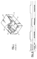
- Fig. 1 is a perspective view of a portion of a prior art ink jet pen.
- Fig. 2 is a circuit diagram of a first embodiment of ink jet pen in which an X-Y matrix selectively drives heater resistor pairs located at each ink jet ejection nozzle.
- Fig. 3 is a waveform diagram illustrating signal levels applied to the X-Y lines of Fig. 2.
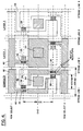
- Fig. 4 is a planar view of multiple circuit levels of a pair of heater resistors that are off-set from each other when viewed from the ink jet ejection nozzle.
- Fig. 5 is a planar view of multiple circuit levels of a pair of heater resistors that are overlaid upon each other when viewed from the ink jet ejection nozzle.
- Fig. 6 is a circuit diagram of a second embodiment of ink jet pen in which an X-Y matrix selectively drives heater resistor pairs located at each ink jet ejection nozzle, without requiring electrical connection between a plurality of circuit layers.
- Fig. 1 illustrates a portion of a prior art ink jet pen and shows a representative ink jet nozzle and its underlying structure.
- a substrate 10 supports a barrier plate 12 which isolates an ink chamber 13 from adjacent ink chambers. Barrier plate 12 further provides an input channel 14 which enables a quantum of ink to be fed into ink chamber 13 and to overlay a heater resistor 16.
- a nozzle plate 18 forms the ink jet emitting surface and includes a nozzle 20 directly aligned over chamber 13 and heater resistor 16. When an appropriate current is applied to heater resistor 16, an amount of energy equal to or greater than E min is applied to the ink within chamber 13, causing the ink to be ejected through nozzle 20 towards a media sheet.
- the preferred embodiment provides a pair of resistors at each chamber which are driven in a half-select manner to enable sufficient power to be coupled to the ink in the chamber to enable that ink to be ejected through nozzle 20.
- half-select does not necessarily mean that exactly 1/2 the power is supplied by each resistor of the pair, but rather that each resistor provides a proportion of the applied power, with the proportion being less than that required to cause a level of thermal energy E min to be coupled to the ink within chamber 13.
- both resistors of the pair are supplied with current simultaneously (or substantially simultaneously) is sufficient energy coupled into the ink positioned in chamber 13 to cause it to be ejected from nozzle 20.
- an X-Y matrix drive circuit 24 which enables ink jet ejection nozzles in a multicolor ink jet pen to be selectively addressed, using the preferred dual resistor addressing arrangement.
- Each nozzle/chamber has a pair of resistors 26 and 28 positioned beneath the chamber and connected so as to the simultaneously driven by row and column drive circuits.
- each of resistors 26 in a first row 30 is connected between a row select conductor 32 and a ground conductor 34.
- a half select drive voltage is applied to row select conductor 32, a half-select current is driven through each of resistors 26 to cause a heating thereof.
- the thermal energy imparted by each of resistors 26 to their associated ink reservoir chambers 13 is less than E min .
- Column selection is achieved by applying one or more strobe pulses to column lines 36.
- Each column line 36 connects to a plurality of resistors 28 whose other terminals are connected to an associated ground conductor (e.g. 34).
- each resistor 28 associated with the energized strobe line has a voltage applied thereacross which causes a half-select current to flow therein. That current causes a heating of a resistor 28 which, in combination with the heat energy dissipated by resistor 26 at a fully selected chamber 13, causes the thermal energy coupled to the ink in chamber 13 to equal or exceed the value E min . Under such circumstances, an ink droplet is ejected from nozzle 20 towards the media sheet.
- the circuit shown in Fig. 2 enables half select addressing of a full-color (black, cyan, magenta, and yellow) ink jet pen using dual resistor addressing.
- the waveforms shown in Fig. 3 illustrate the signals which implement the half-select addressing action.
- a plan view shows a substrate structure which configures the dual resistor drive arrangement.
- dual resistors 26, 28 are offset, but adjacent, as viewed from nozzle plate 18.
- the composite view at the left of Fig. 4 illustrates the plural, superposed circuit layers which achieve the dual resistor, half-select operation.
- a contact 50 enables connection of a ground conductor to each of heater resistors 26, 28.
- Each heater resistor 28 is connected via a conductor 56 to a strobe line 58.
- each heater resistor 26 is connected by a conductor 60 to a row drive conductor 62. Note that heater resistors 26 and 28 are on different levels of metallization, but are placed adjacent each other and directly beneath an ink chamber.
- FIG. 4 To the right of the composite plan view of Fig. 4, is a view of "Layer 1" metallization showing how the row drive conductors 62 connect to heater resistors 26 and to ground contact 50.
- the illustration of the "Layer 2" metallization shows how heater resistors 28 connect to column strobe lines 58 for column selection.
- Fig. 5 a similar structure to Fig. 4 is shown, however, heater resistors 26 and 28 are superposed over one another at each chamber and are separated by a dielectric layer (not shown).
- a dielectric layer not shown.
- FIG. 6 another embodiment is illustrated in which inter-circuit layer connections are not required. While heater resistors 70 are connected in parallel between parallel arranged strobe and ground conductors, heater resistors 72 are connected in series along each row of the matrix. Thus, no heater resistor needs to be connected between intersecting row and column conductors.
- the serial resistor connection may dictate a shorter string of heater resistors 72 connected to a row select driver to assure sufficient thermal emission at each heater resistor 72.
- thermal multiplexing arrangement enables a reduction of total signal lines and further enables the ink jet cells to be produced on relatively inexpensive substrates (e.g. ceramics or glass).
Applications Claiming Priority (2)
| Application Number | Priority Date | Filing Date | Title |
|---|---|---|---|
| US58907396A | 1996-01-23 | 1996-01-23 | |
| US589073 | 1996-01-23 |
Publications (3)
| Publication Number | Publication Date |
|---|---|
| EP0786343A2 true EP0786343A2 (fr) | 1997-07-30 |
| EP0786343A3 EP0786343A3 (fr) | 1998-05-20 |
| EP0786343B1 EP0786343B1 (fr) | 2001-06-13 |
Family
ID=24356484
Family Applications (1)
| Application Number | Title | Priority Date | Filing Date |
|---|---|---|---|
| EP97300095A Expired - Lifetime EP0786343B1 (fr) | 1996-01-23 | 1997-01-09 | Dispositif d'impression thermique par jet d'encre et méthode d'actionnement |
Country Status (4)
| Country | Link |
|---|---|
| US (1) | US6007186A (fr) |
| EP (1) | EP0786343B1 (fr) |
| JP (1) | JPH09193387A (fr) |
| DE (1) | DE69705132T2 (fr) |
Cited By (1)
| Publication number | Priority date | Publication date | Assignee | Title |
|---|---|---|---|---|
| EP1080903A3 (fr) * | 1999-08-30 | 2001-05-02 | Hewlett-Packard Company, A Delaware Corporation | Retours communs à la base multi-bornes pour tête d'impression à jet d'encre |
Families Citing this family (9)
| Publication number | Priority date | Publication date | Assignee | Title |
|---|---|---|---|---|
| US6828049B2 (en) * | 2001-10-29 | 2004-12-07 | Hewlett-Packard Development Company, L.P. | Replaceable fuel cell apparatus having information storage device |
| US6713201B2 (en) | 2001-10-29 | 2004-03-30 | Hewlett-Packard Development Company, L.P. | Systems including replaceable fuel cell apparatus and methods of using replaceable fuel cell apparatus |
| US20030138679A1 (en) * | 2002-01-22 | 2003-07-24 | Ravi Prased | Fuel cartridge and reaction chamber |
| US6887596B2 (en) | 2002-01-22 | 2005-05-03 | Hewlett-Packard Development Company, L.P. | Portable disposable fuel-battery unit for a fuel cell system |
| US7731491B2 (en) * | 2002-10-16 | 2010-06-08 | Hewlett-Packard Development Company, L.P. | Fuel storage devices and apparatus including the same |
| US6989210B2 (en) * | 2003-04-23 | 2006-01-24 | Hewlett-Packard Development Company, L.P. | Fuel cartridge with thermo-degradable barrier system |
| US7489859B2 (en) * | 2003-10-09 | 2009-02-10 | Hewlett-Packard Development Company, L.P. | Fuel storage devices and apparatus including the same |
| US8084150B2 (en) * | 2004-04-28 | 2011-12-27 | Eveready Battery Company, Inc. | Fuel cartridges and apparatus including the same |
| EP2237957B1 (fr) * | 2008-01-28 | 2014-03-12 | Hewlett-Packard Development Company, L.P. | Circuit transistor à jonction bipolaire latérale à base commune pour une tête d'impression à jet d'encre |
Citations (3)
| Publication number | Priority date | Publication date | Assignee | Title |
|---|---|---|---|---|
| US4695853A (en) | 1986-12-12 | 1987-09-22 | Hewlett-Packard Company | Thin film vertical resistor devices for a thermal ink jet printhead and methods of manufacture |
| US5103246A (en) | 1989-12-11 | 1992-04-07 | Hewlett-Packard Company | X-Y multiplex drive circuit and associated ink feed connection for maximizing packing density on thermal ink jet (TIJ) printheads |
| US5134425A (en) | 1990-01-23 | 1992-07-28 | Hewlett-Packard Company | Ohmic heating matrix |
Family Cites Families (3)
| Publication number | Priority date | Publication date | Assignee | Title |
|---|---|---|---|---|
| AU531269B2 (en) * | 1979-03-06 | 1983-08-18 | Canon Kabushiki Kaisha | Ink jet printer |
| EP0317171A3 (fr) * | 1987-11-13 | 1990-07-18 | Hewlett-Packard Company | Système d'injection intégral à couches minces pour une tête imprimante à projection thermique et méthodes d'opération |
| US5479196A (en) * | 1990-02-26 | 1995-12-26 | Canon Kabushiki Kaisha | Ink jet recording apparatus and method of recovery ink discharging condition of the same |
-
1997
- 1997-01-09 EP EP97300095A patent/EP0786343B1/fr not_active Expired - Lifetime
- 1997-01-09 DE DE69705132T patent/DE69705132T2/de not_active Expired - Fee Related
- 1997-01-21 JP JP9008406A patent/JPH09193387A/ja active Pending
-
1999
- 1999-02-04 US US09/276,090 patent/US6007186A/en not_active Expired - Lifetime
Patent Citations (3)
| Publication number | Priority date | Publication date | Assignee | Title |
|---|---|---|---|---|
| US4695853A (en) | 1986-12-12 | 1987-09-22 | Hewlett-Packard Company | Thin film vertical resistor devices for a thermal ink jet printhead and methods of manufacture |
| US5103246A (en) | 1989-12-11 | 1992-04-07 | Hewlett-Packard Company | X-Y multiplex drive circuit and associated ink feed connection for maximizing packing density on thermal ink jet (TIJ) printheads |
| US5134425A (en) | 1990-01-23 | 1992-07-28 | Hewlett-Packard Company | Ohmic heating matrix |
Cited By (2)
| Publication number | Priority date | Publication date | Assignee | Title |
|---|---|---|---|---|
| EP1080903A3 (fr) * | 1999-08-30 | 2001-05-02 | Hewlett-Packard Company, A Delaware Corporation | Retours communs à la base multi-bornes pour tête d'impression à jet d'encre |
| EP1520702A1 (fr) * | 1999-08-30 | 2005-04-06 | Hewlett-Packard Company | Retours communs à la base multi-bornes pour tête d'impression à jet d'encre |
Also Published As
| Publication number | Publication date |
|---|---|
| US6007186A (en) | 1999-12-28 |
| DE69705132T2 (de) | 2001-09-27 |
| EP0786343A3 (fr) | 1998-05-20 |
| DE69705132D1 (de) | 2001-07-19 |
| EP0786343B1 (fr) | 2001-06-13 |
| JPH09193387A (ja) | 1997-07-29 |
Similar Documents
| Publication | Publication Date | Title |
|---|---|---|
| EP1080898B1 (fr) | Trajets de signaux d'entrée redondants pour une imprimante à jet d'encre | |
| US6332677B1 (en) | Stable substrate structure for a wide swath nozzle array in a high resolution inkjet printer | |
| US4999650A (en) | Bubble jet print head having improved multiplex actuation construction | |
| EP0289347B1 (fr) | Tête d'impression thermique à jet d'encre | |
| US6290334B1 (en) | Recording apparatus, recording head and substrate therefor | |
| US5057855A (en) | Thermal ink jet printhead and control arrangement therefor | |
| KR100871543B1 (ko) | 잉크젯 프린팅 시스템 및 잉크젯 프린트헤드 | |
| US8246135B2 (en) | Headchip and head for array type inkjet printer | |
| US5134425A (en) | Ohmic heating matrix | |
| KR20080070603A (ko) | 잉크젯 프린트헤드 및 방울 발생기를 선택적으로활성화하는 방법 | |
| JPH07169609A (ja) | 受動多重化抵抗器アレイ | |
| EP0786343B1 (fr) | Dispositif d'impression thermique par jet d'encre et méthode d'actionnement | |
| KR100754644B1 (ko) | 잉크젯 프린트헤드와 잉크젯 카트리지 및 잉크 방울 부착 방법 | |
| NZ523870A (en) | Narrow multi-color ink jet printhead | |
| US5508724A (en) | Passive multiplexing using sparse arrays | |
| US7488056B2 (en) | Fluid ejection device | |
| KR20020033544A (ko) | 잉크젯 프린트헤드 및 그 작동 방법 | |
| JPH0994968A (ja) | インクジェットプリントヘッド | |
| US6851791B2 (en) | Polychromatic printhead | |
| MXPA06012022A (en) | Fluid ejection device |
Legal Events
| Date | Code | Title | Description |
|---|---|---|---|
| PUAI | Public reference made under article 153(3) epc to a published international application that has entered the european phase |
Free format text: ORIGINAL CODE: 0009012 |
|
| AK | Designated contracting states |
Kind code of ref document: A2 Designated state(s): DE FR GB IT |
|
| PUAL | Search report despatched |
Free format text: ORIGINAL CODE: 0009013 |
|
| AK | Designated contracting states |
Kind code of ref document: A3 Designated state(s): DE FR GB IT |
|
| 17P | Request for examination filed |
Effective date: 19980911 |
|
| 17Q | First examination report despatched |
Effective date: 19981030 |
|
| GRAG | Despatch of communication of intention to grant |
Free format text: ORIGINAL CODE: EPIDOS AGRA |
|
| GRAG | Despatch of communication of intention to grant |
Free format text: ORIGINAL CODE: EPIDOS AGRA |
|
| GRAH | Despatch of communication of intention to grant a patent |
Free format text: ORIGINAL CODE: EPIDOS IGRA |
|
| GRAH | Despatch of communication of intention to grant a patent |
Free format text: ORIGINAL CODE: EPIDOS IGRA |
|
| RAP1 | Party data changed (applicant data changed or rights of an application transferred) |
Owner name: HEWLETT-PACKARD COMPANY, A DELAWARE CORPORATION |
|
| GRAA | (expected) grant |
Free format text: ORIGINAL CODE: 0009210 |
|
| AK | Designated contracting states |
Kind code of ref document: B1 Designated state(s): DE FR GB IT |
|
| PG25 | Lapsed in a contracting state [announced via postgrant information from national office to epo] |
Ref country code: IT Free format text: LAPSE BECAUSE OF FAILURE TO SUBMIT A TRANSLATION OF THE DESCRIPTION OR TO PAY THE FEE WITHIN THE PRESCRIBED TIME-LIMIT;WARNING: LAPSES OF ITALIAN PATENTS WITH EFFECTIVE DATE BEFORE 2007 MAY HAVE OCCURRED AT ANY TIME BEFORE 2007. THE CORRECT EFFECTIVE DATE MAY BE DIFFERENT FROM THE ONE RECORDED. Effective date: 20010613 |
|
| REF | Corresponds to: |
Ref document number: 69705132 Country of ref document: DE Date of ref document: 20010719 |
|
| ET | Fr: translation filed | ||
| REG | Reference to a national code |
Ref country code: GB Ref legal event code: IF02 |
|
| PLBE | No opposition filed within time limit |
Free format text: ORIGINAL CODE: 0009261 |
|
| STAA | Information on the status of an ep patent application or granted ep patent |
Free format text: STATUS: NO OPPOSITION FILED WITHIN TIME LIMIT |
|
| 26N | No opposition filed | ||
| PGFP | Annual fee paid to national office [announced via postgrant information from national office to epo] |
Ref country code: FR Payment date: 20070207 Year of fee payment: 11 |
|
| PGFP | Annual fee paid to national office [announced via postgrant information from national office to epo] |
Ref country code: GB Payment date: 20080129 Year of fee payment: 12 |
|
| PGFP | Annual fee paid to national office [announced via postgrant information from national office to epo] |
Ref country code: DE Payment date: 20080229 Year of fee payment: 12 |
|
| REG | Reference to a national code |
Ref country code: FR Ref legal event code: ST Effective date: 20081029 |
|
| PG25 | Lapsed in a contracting state [announced via postgrant information from national office to epo] |
Ref country code: FR Free format text: LAPSE BECAUSE OF NON-PAYMENT OF DUE FEES Effective date: 20080131 |
|
| GBPC | Gb: european patent ceased through non-payment of renewal fee |
Effective date: 20090109 |
|
| PG25 | Lapsed in a contracting state [announced via postgrant information from national office to epo] |
Ref country code: DE Free format text: LAPSE BECAUSE OF NON-PAYMENT OF DUE FEES Effective date: 20090801 |
|
| PG25 | Lapsed in a contracting state [announced via postgrant information from national office to epo] |
Ref country code: GB Free format text: LAPSE BECAUSE OF NON-PAYMENT OF DUE FEES Effective date: 20090109 |