EP0785410B1 - Probe, method of manufacturing the probe, probe unit, and information recording/reproducing apparatus using the probe unit - Google Patents
Probe, method of manufacturing the probe, probe unit, and information recording/reproducing apparatus using the probe unit Download PDFInfo
- Publication number
- EP0785410B1 EP0785410B1 EP97100739A EP97100739A EP0785410B1 EP 0785410 B1 EP0785410 B1 EP 0785410B1 EP 97100739 A EP97100739 A EP 97100739A EP 97100739 A EP97100739 A EP 97100739A EP 0785410 B1 EP0785410 B1 EP 0785410B1
- Authority
- EP
- European Patent Office
- Prior art keywords
- cantilever
- tip
- probe
- substrate
- layer
- Prior art date
- Legal status (The legal status is an assumption and is not a legal conclusion. Google has not performed a legal analysis and makes no representation as to the accuracy of the status listed.)
- Expired - Lifetime
Links
Images


Classifications
-
- G—PHYSICS
- G11—INFORMATION STORAGE
- G11B—INFORMATION STORAGE BASED ON RELATIVE MOVEMENT BETWEEN RECORD CARRIER AND TRANSDUCER
- G11B9/00—Recording or reproducing using a method not covered by one of the main groups G11B3/00 - G11B7/00; Record carriers therefor
- G11B9/12—Recording or reproducing using a method not covered by one of the main groups G11B3/00 - G11B7/00; Record carriers therefor using near-field interactions; Record carriers therefor
- G11B9/14—Recording or reproducing using a method not covered by one of the main groups G11B3/00 - G11B7/00; Record carriers therefor using near-field interactions; Record carriers therefor using microscopic probe means, i.e. recording or reproducing by means directly associated with the tip of a microscopic electrical probe as used in Scanning Tunneling Microscopy [STM] or Atomic Force Microscopy [AFM] for inducing physical or electrical perturbations in a recording medium; Record carriers or media specially adapted for such transducing of information
- G11B9/1409—Heads
-
- G—PHYSICS
- G01—MEASURING; TESTING
- G01Q—SCANNING-PROBE TECHNIQUES OR APPARATUS; APPLICATIONS OF SCANNING-PROBE TECHNIQUES, e.g. SCANNING PROBE MICROSCOPY [SPM]
- G01Q60/00—Particular types of SPM [Scanning Probe Microscopy] or microscopes; Essential components thereof
- G01Q60/02—Multiple-type SPM, i.e. involving more than one SPM techniques
- G01Q60/04—STM [Scanning Tunnelling Microscopy] combined with AFM [Atomic Force Microscopy]
-
- G—PHYSICS
- G01—MEASURING; TESTING
- G01Q—SCANNING-PROBE TECHNIQUES OR APPARATUS; APPLICATIONS OF SCANNING-PROBE TECHNIQUES, e.g. SCANNING PROBE MICROSCOPY [SPM]
- G01Q70/00—General aspects of SPM probes, their manufacture or their related instrumentation, insofar as they are not specially adapted to a single SPM technique covered by group G01Q60/00
- G01Q70/08—Probe characteristics
- G01Q70/14—Particular materials
-
- G—PHYSICS
- G11—INFORMATION STORAGE
- G11B—INFORMATION STORAGE BASED ON RELATIVE MOVEMENT BETWEEN RECORD CARRIER AND TRANSDUCER
- G11B9/00—Recording or reproducing using a method not covered by one of the main groups G11B3/00 - G11B7/00; Record carriers therefor
- G11B9/12—Recording or reproducing using a method not covered by one of the main groups G11B3/00 - G11B7/00; Record carriers therefor using near-field interactions; Record carriers therefor
- G11B9/14—Recording or reproducing using a method not covered by one of the main groups G11B3/00 - G11B7/00; Record carriers therefor using near-field interactions; Record carriers therefor using microscopic probe means, i.e. recording or reproducing by means directly associated with the tip of a microscopic electrical probe as used in Scanning Tunneling Microscopy [STM] or Atomic Force Microscopy [AFM] for inducing physical or electrical perturbations in a recording medium; Record carriers or media specially adapted for such transducing of information
- G11B9/1418—Disposition or mounting of heads or record carriers
-
- B—PERFORMING OPERATIONS; TRANSPORTING
- B82—NANOTECHNOLOGY
- B82Y—SPECIFIC USES OR APPLICATIONS OF NANOSTRUCTURES; MEASUREMENT OR ANALYSIS OF NANOSTRUCTURES; MANUFACTURE OR TREATMENT OF NANOSTRUCTURES
- B82Y10/00—Nanotechnology for information processing, storage or transmission, e.g. quantum computing or single electron logic
-
- Y—GENERAL TAGGING OF NEW TECHNOLOGICAL DEVELOPMENTS; GENERAL TAGGING OF CROSS-SECTIONAL TECHNOLOGIES SPANNING OVER SEVERAL SECTIONS OF THE IPC; TECHNICAL SUBJECTS COVERED BY FORMER USPC CROSS-REFERENCE ART COLLECTIONS [XRACs] AND DIGESTS
- Y10—TECHNICAL SUBJECTS COVERED BY FORMER USPC
- Y10S—TECHNICAL SUBJECTS COVERED BY FORMER USPC CROSS-REFERENCE ART COLLECTIONS [XRACs] AND DIGESTS
- Y10S977/00—Nanotechnology
- Y10S977/84—Manufacture, treatment, or detection of nanostructure
- Y10S977/849—Manufacture, treatment, or detection of nanostructure with scanning probe
- Y10S977/86—Scanning probe structure
- Y10S977/873—Tip holder
Definitions
- the present invention relates to a probe used in a scanning probe microscope, a method of manufacturing the probe, a probe unit, and an information recording/reproducing apparatus using the probe unit.
- a scanning tunnel microscope (to be abbreviated as an STM hereinafter) and a scanning atomic force microscope (to be abbreviated as an AFM hereinafter) are put into practical use (a scanning probe microscope (to be abbreviated as an SPM hereinafter) is a general term for these microscopes).
- a tip can access a sample surface on an atomic level. Therefore, it is being attempted to apply these SPMs to an information recording/reproducing apparatus which writes recording information in a local region.
- the STM detects a tunnel current flowing when the distance between a biased conductive tip and a conductive sample is decreased to a few ⁇ or smaller, scans the tip while controlling the distance between the tip and the sample so that the tunnel current is held constant, and forms an image of the tunnel current or of a feedback control signal, thereby constructing the surface image.
- Examples of a recording method using the STM are a method in which a voltage is applied between a tip and a recording medium to locally change the surface state of the recording medium, and a method in which the conductivity of a recording medium is changed.
- the AFM detects an atomic force acting between a tip and the surface of a sample when the tip is approached to a distance of several ⁇ or less from the sample, and scans the tip in a two-dimensional plane, thereby constructing the surface image containing undulation information.
- an elastic cantilever which has one fixed end and holds the tip in the vicinity of the free end is used.
- a scanning atomic force/tunnel composite microscope is an example of a multifunctional microscope for singly performing AFM and STM observations.
- a probe used in the AFM consists of a cantilever and a tip held by the cantilever.
- the tip is made from a conductive material, and this allows the microscope to detect a current flowing between the tip and a sample.
- the microscope can detect a current by applying a bias between the tip and a sample during an AFM operation and can simultaneously obtain a surface undulation image and a tunnel current distribution image by using the same tip.
- this composite apparatus Since the tip of this composite apparatus can also access the sample surface on an atomic level, it is being tried to apply the composite apparatus to an information recording/reproducing apparatus which writes recording information in a local region.
- FIG. 1A A conventional probe formation method (U.S.P. No. 5,221,415) is shown in Figs. 1A to 1G.
- crystallographic axis anisotropic etching is performed for a single-crystal Si substrate 202 on which an Si oxide film 201 is formed, thereby forming a recessed portion 203 with an inverse pyramid shape (Fig. 1A).
- the Si oxide film 201 is removed.
- this recessed portion 203 By using this recessed portion 203 as a female mold, all surfaces are covered with a silicon nitride layer 204 (Fig. 1B).
- This silicon nitride layer 204 is patterned into the shape of a cantilever 205 (Fig. 1C).
- a glass plate 208 having a saw-cut groove 206 and a Cr layer 207 is joined to the silicon nitride layer 204 (Fig. 1D).
- a portion of the glass plate 208 is cut away (Fig. 1E).
- the single-crystal Si substrate 202 is etched away to form a cantilever probe 209 (Fig. 1F).
- a metal layer 210 serving as an optical lever type AFM reflecting film is formed.
- a tip formation method examples include Figs. 2A and 2B.
- a thin-film layer 211 is patterned into the shape of a circle on the substrate, silicon 212 is etched by using the circular layer 211, and a tip 213 is formed by using side etching (O. Wolter et al., "Micromachined silicon sensors for scanning forcemicroscopy", J. Vac. Sci. Technol. B9(2), Mar/Apr, 1991, pp. 1353-1357).
- side etching O. Wolter et al., "Micromachined silicon sensors for scanning forcemicroscopy", J. Vac. Sci. Technol. B9(2), Mar/Apr, 1991, pp. 1353-1357.
- a conductive material 215 is obliquely deposited in an inversely tapered resist hole 214 while the substrate is rotated, and a tip 213 is formed by lifting off the conductive material (C.A. Spindt et al., "Physical properties of thin film field emission cathode with molybdenum cones", J. Appl. Phys., 47, 1976, pp. 5248-5263).
- a stress occurs between the cantilever and the metal film and this warps the cantilever. If the cantilever warps toward a tip and the point of the cantilever warps to the opposite side, there is the possibility that a middle portion of the cantilever comes in contact with a sample or a recording medium. This is particularly a problem when a plurality of probes are used since warp variations take place. That is, in an information processing apparatus using the principle of AFM/STM, a plurality of probes in the same plane are to be simultaneously brought into contact with a recording medium. If these levers have warp variations, the levers apply different loads on the recording medium. Depending on the magnitudes of these loads, the resolution is decreased or the recording medium or the point of the tip is broken.
- the tip itself has the following problem.
- an STM probe is manufactured by coating a cantilever probe with a conductive material
- the point of the tip is difficult to coat since the point is formed to be sharp. Consequently, it is difficult to obtain stable characteristics in the STM which handles a weak current called a tunnel current.
- a tunnel current For example, in the tips shown in Figs. 2A and 2B, the resist patterning conditions and the etching conditions of the materials when the tips are formed are difficult to hold constant. This results in the problem that it is difficult to accurately maintain the heights of a plurality of tips formed and the shapes such as the radius of curvature of the point.
- an object of the present invention to solve the above conventional problems and provide a probe in which a cantilever itself has no warp and does not warp due to an electrode line, an electrode area can be decreased, a stray capacitance between the cantilever and a recording medium can be reduced, the recording speed can be increased, the cantilever is not broken by a stress, a conductive metal tip having a sharp point can be formed on the cantilever with a high reproducibility, the weight can be decreased, and the metal tip can be easily formed in a desired position, a method of manufacturing the probe, a probe unit, and an information recording/reproducing apparatus using the probe unit.
- the above object of the present invention is achieved by a method of manufacturing a probe according to claim 3.
- the above object of the present invention is achieved by an information recording/reproducing apparatus for performing recording and reproduction of information on a recording medium according to claim 5.
- Figs. 3A and 3B are sectional and plan views, respectively, of a probe of the present invention.
- a single-crystal Si substrate 101 and a single-crystal Si cantilever 102 are arranged via an SiO 2 layer 103.
- An impurity is doped in the single-crystal Si cantilever 102 to extract a tunnel current.
- a metal tip 105 is formed on a free end portion of the cantilever 102.
- a metal silicide layer 104 made from the same materials as the cantilever 102 and the tip 105 is formed at the interface between the cantilever 102 and the tip 105.
- An electrode line 106 is formed on the other end of the cantilever 102.
- the Si cantilever 102 is used as a tunnel current extracting line, no warp occurs in the cantilever due to the electrode line.
- a tunnel current is extracted from the Si cantilever 102 by using the electrode line 106. This decreases the electrode area when compared to a probe in which a cantilever and an entire surface of a substrate holding the cantilever are coated with a conductive material.
- Figs. 4A to 4F illustrate a method of manufacturing the probe of the present invention.
- a substrate obtained by forming an SiO 2 layer 103 and a single-crystal Si layer 107 on a single-crystal Si substrate 101 i.e., an SOI (Silicon On Insulator) substrate, is coated with a silicon nitride (SiN) layer 108 (Fig. 4A).
- SOI Silicon On Insulator
- This single-crystal Si layer 107 is doped with an impurity and having a low resistance.
- the resistivity is preferably 0.01 ⁇ cm or less.
- the thickness of the single-crystal Si layer 107 is determined together with the shape of a desired cantilever with respect to the spring constant of the cantilever.
- the thickness is usually 0.1 to several ⁇ m.
- the SiO 2 layer 103 and the SiN layer 108 need only have thicknesses which can resist etching using an aqueous potassium hydroxide solution performed later.
- the thickness of the SiO 2 layer 103 is about 0.1 to 1.0 ⁇ m
- the thickness of the SiN layer 108 is 0.1 to 0.3 ⁇ m.
- the SiN layer 108 in a lever formation portion on the back side of the substrate and the SiN layer 108 on the entire upper surface are removed by dry etching.
- the single-crystal Si layer 107 is processed into the shape of a cantilever 102 (Fig. 4B).
- An electrode line 106 for extracting a tunnel current from the cantilever 102 is formed in one end of the cantilever 102 (Fig. 4C).
- the cantilever 102 functions as a tunnel current extracting electrode and a mechanical elastic member.
- a tip is formed on another substrate.
- An SiO 2 layer or SiN layer 112 on a (100) Si substrate 111 is removed into the shape of a rectangle or a circle to expose the Si surface. Crystallographic axis anisotropic etching is performed for the exposed Si surface by using an aqueous potassium hydroxide solution, forming a recessed portion 113 (Fig. 5A).
- the substrate is again covered with a thin SiO 2 layer 114 (Fig. 5C).
- a tip material film 115 is formed on the substrate (Fig. 5D) and patterned to form a tip 105 (Fig. 5E).
- the tip material is a metal capable of extracting a tunnel current. It is possible to preferably use Au or Pt which does not easily form an oxide film or Ir having a high mechanical strength.
- the tip 105 is then transferred onto the cantilever 102.
- a method of transferring and joining the tip 105 is as follows (Figs. 6A and 6B). First, a natural SiO film on the surface of the cantilever 102 is removed by a buffer hydrofluoric acid (BHF), and the two substrates are positioned.
- BHF buffer hydrofluoric acid
- a metal silicide layer 104 (Fig. 6A).
- the tip and the cantilever are strongly joined and are not peeled from each other. Thereafter, the tip 105 is transferred onto the cantilever 102 by peeling the substrate (Fig. 6B).
- a warp of the cantilever caused by a film stress can be avoided because the single-crystal cantilever is used and the tip is transferred only to the distal end of the cantilever.
- a protective layer 109 such as a resist or a polyimide resin is formed to protect the surface from contamination (Fig. 4D).
- the Si exposed surface on the back side of the Si substrate 101 is subjected to crystallographic axis anisotropic etching by using an aqueous potassium hydroxide solution subjected to heating (Fig. 4E).
- the exposed SiO 2 layer 103 is dissolved away by a BHF solution and subsequently the protective film 109 is removed by an oxygen plasma treatment, thereby obtaining a desired probe 110 (Fig. 4F).
- the tip thus formed has a hollow region and hence is lighter than that of a tip shown in Fig. 2B.
- the tip can be adhered to any place on the cantilever and this increases the allowance of the manufacturing process.
- a 0.2- ⁇ m thick silicon nitride (SiN) layer 108 was formed by LP-CVD (Low Pressure Chemical Vapor Deposition) on an SOI (Silicon On Insulator) substrate manufactured by forming a 0.5- ⁇ m thick SiO 2 layer 103 and a 1.0- ⁇ m thick single-crystal Si layer 107 on a (100) Si substrate 101 (Fig. 4A).
- the single-crystal Si layer 107 used had a resistivity of 0.01 ⁇ cm or less.
- a resist pattern was formed on the back side to etch the Si substrate 101, and the SiN layer 108 was patterned by dry etching using CF 4 gas.
- the SiN layer 108 on the entire upper surface was etched away, and the single-crystal Si layer 107 was patterned into the shape of a cantilever 102 by photolithography and etching (Fig. 4B).
- the cantilever shape was a rectangle 250 ⁇ m long and 40 ⁇ m wide.
- An electrode line 106 for extracting a tunnel current was then formed on an end portion of the cantilever 102 (Fig. 4C).
- a 0.1- ⁇ m thick SiO 2 layer 112 was formed on a (100) Si substrate 111.
- a hole with a diameter of 6 ⁇ m was formed in this SiO 2 layer 112 by photolithography and etching.
- the resultant substrate was subjected to crystallographic axis anisotropic etching by using an aqueous potassium hydroxide solution, forming an inverse triangular recessed portion 113 in the hole (Fig. 5A).
- the substrate was dipped into a BHF solution to dissolve away the SiO 2 layer 112 (Fig. 5B).
- the resultant substrate was then heated in an oxidizing atmosphere to form a 100-nm thick SiO 2 layer 114 on all the surfaces of the substrate (Fig. 5C).
- a 1- ⁇ m thick Au film 115 as a tip material was formed on the substrate (Fig. 5D) and patterned by photolithography and etching, thereby forming a tip 105 (Fig. 5E).
- a natural oxide film on the surface of the cantilever 102 was removed by dipping the cantilever 102 into a BHF solution.
- the substrate on which the cantilever 102 was formed and the substrate on which the tip 105 was formed were positioned.
- the two substrates are brought into contact with each other under pressure (Fig. 6A).
- a 5- ⁇ m thick polyimide layer 109 was formed as a protective film on the surface of the substrate where the cantilever 102 and the tip 105 were formed (Fig. 4D).
- the lower surface of the substrate was dipped into an aqueous potassium hydroxide solution to perform crystallographic axis anisotropic etching (Fig. 4E).
- the exposed SiO 2 layer 103 was dissolved away with a BHF solution.
- the cleavage plane of an HOPG (High Orientation Pyrolytic Graphite) substrate was observed with a scan area of 1000 ⁇ x 1000 ⁇ by an AFM/STM apparatus. Consequently, good surface information could by obtained with a high reproducibility.
- HOPG High Orientation Pyrolytic Graphite
- a 0.2- ⁇ m thick SiN layer 108 was formed on an SOI substrate (Fig. 4A).
- a single-crystal Si layer 107 having a resistivity of 0.01 ⁇ cm or less was used.
- the SiN layer 108 on the back side was patterned and the SiN layer 108 on the entire upper surface was removed by etching. Thereafter, the single-crystal Si layer 107 was patterned into the shape of a cantilever 102 by photolithography and etching (Fig. 4B).
- the lever shape was a rectangle 200 ⁇ m long and 50 ⁇ m wide.
- an electrode line 106 for extracting a tunnel current was formed on an end portion of the cantilever 102 fixed on the SiO 2 layer (Fig. 4C).
- a tip 105 was formed following the same procedure as in Example 1.
- Pt was used as the tip material.
- a natural oxide film on the surface of the cantilever 102 was removed by dipping the cantilever 102 into a BHF solution.
- the substrate on which the cantilever 102 was formed and the substrate on which the tip 105 was formed were positioned, and the two substrates were joined under pressure (Fig. 6A).
- the substrates were heated to 150°C.
- the tip 105 was well formed on the cantilever 102 (Fig. 6B).
- a 5- ⁇ m thick polyimide layer 109 was formed as a protective film on the surface of the substrate where the cantilever 102 and the tip 105 were formed (Fig. 4D).
- the lower surface of the substrate was dipped into an aqueous potassium hydroxide solution to perform crystallographic axis anisotropic etching (Fig. 4E).
- the exposed SiO 2 layer 103 was dissolved away with a BHF solution.
- sixteen probes were simultaneously formed on the same substrate by the above formation method. When these probes were measured with a scanning laser microscope, no warp was detected in both the longitudinal and lateral directions of the cantilever of any probe.
- the cleavage plane of an HOPG (High Orientation Pyrolytic Graphite) substrate was observed with a scan area of 1000 ⁇ x 1000 ⁇ by an AFM/STM apparatus. Consequently, good surface information could by obtained with a high reproducibility.
- HOPG High Orientation Pyrolytic Graphite
- a 0.2- ⁇ m thick SiN layer 108 was formed on an SOI substrate (Fig. 4A).
- a single-crystal Si layer 107 having a resistivity of 0.01 ⁇ cm or less was used.
- the SiN layer 108 on the back side was patterned and the SiN layer 108 on the entire upper surface was removed by etching. Thereafter, the single-crystal Si layer 107 was patterned into the shape of a cantilever 102 by photolithography and etching (Fig. 4B).
- the cantilever shape was a rectangle 200 ⁇ m long and 50 ⁇ m wide. Subsequently, an electrode line 106 for extracting a tunnel current was formed on an end portion of the cantilever 102 (Fig. 4C).
- a tip 105 was formed following the same procedure as in Example 1.
- a natural oxide film on the surface of the cantilever 102 was removed by dipping the cantilever 102 into a BHF solution.
- the substrate on which the cantilever 102 was formed and the substrate on which the tip 105 was formed were positioned, and the two substrates were joined under pressure (Fig. 6A).
- the substrates were heated to 120°C.
- the tip 105 was well formed on the cantilever 102 (Fig. 6B).
- a 5- ⁇ m thick polyimide layer 109 was formed as a protective film on the surface of the substrate where the cantilever 102 and the tip 105 were formed (Fig. 4D).
- the lower surface of the substrate was dipped into an aqueous potassium hydroxide solution to perform crystallographic axis anisotropic etching (Fig. 4E).
- the exposed SiO 2 layer 103 was dissolved away with a BHF solution.
- sixteen probes were simultaneously formed on the same substrate by the above formation method. When these probes were measured with a scanning laser microscope, no warp was detected in both the longitudinal and lateral directions of the cantilever of any probe.
- the cleavage plane of an HOPG (High Orientation Pyrolytic Graphite) substrate was observed with a scan area of 1000 ⁇ x 1000 ⁇ by an AFM/STM apparatus. Consequently, good surface information could by obtained with a high reproducibility.
- HOPG High Orientation Pyrolytic Graphite
- FIG. 7 shows the arrangement of major components and a block diagram of the present invention. This example will be described with reference to Fig. 7.
- a probe 118 was arranged to oppose a recording medium 117 on a recording medium stage 116.
- This recording medium 117 consists of an information recording layer 117-1, an underlying electrode 117-2 for applying a voltage to the information recording layer 117-1, and a substrate 117-3.
- the information recording layer 117-1 is, e.g., a thin organic film which changes its electrical properties (an electrical memory effect) due to a tunnel current produced between the layer 117-1 and a tip 119.
- the apparatus also includes a power source 120 and a current amplifier 121 which is connected to a microcomputer 122 and used to record and reproduce information with respect to the recording medium 117.
- the recording medium stage 116 on a recording medium stage drive mechanism 123 is controlled by a position control circuit (Z direction) 124, a position control circuit (X-Y direction) 125, a tilt angle control circuit 126, and a rotation angle control circuit 127 under the control of the microcomputer 122.
- a laser 128 is irradiated on the point of the probe 118, the reflected light is received by a split sensor 129, and the deflection of the probe 118 is detected by a deflection detecting device 130.
- This information is supplied to the microcomputer 122 and a servo circuit 131.
- the recording medium 117 of this example was manufactured by depositing a 30-nm thick Au film as the underlaying electrode 117-2 on the silica glass substrate 117-3 by vacuum deposition and forming a polyimide layer (the information recording layer 117-1) on top of the underlying electrode 117-2 by an LB (Langmuir-Blodgett) technique.
- the probes 118 manufactured in the first example were incorporated into the recording/reproducing apparatus described above, and recording and reproduction were performed by a principle and a method disclosed in Japanese Laid-Open Patent Application No. 63-161552. Consequently, good AFM images could be obtained with all of the probes 118, and damages, e.g., film peeling, to the recording medium 117 were not observed.
- a pulse voltage was applied between the tip 119 and the underlying electrode 117-2.
- the application of the voltage was done by using a 3-V pulse rectangular wave with a width of 50 ns.
- the recording medium was scanned with a DC voltage of 200 mV. As a consequence, the characteristics changed in the pulse application point of the information recording layer 117-1 to produce a portion where the electrical resistance was low.
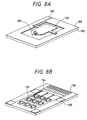
- Fig. 8A is a perspective view of the structure.
- the lever dimensions were a length of 300 ⁇ m and a width of 150 ⁇ m.
- a signal processing IC 134 On the same substrate, a signal processing IC 134, a surface aligning mechanism 135, and signal extracting pads 136 were formed (Fig. 8B).
- An IC formed on an SOI substrate has a low leakage current and hence does not easily cause a processing error when compared to an IC formed on a common Si wafer.
- This probe unit was used to perform recording and reproduction in the same manner as in Example 4, and it was found that the recording and reproduction could be well performed with all the probes.
- a cantilever itself has almost no warp because the cantilever is made from single-crystal Si. Also, since the cantilever is conductive, no new electrode line needs to be formed and this prevents a warp of the lever resulting from an electrode line.
- the cantilever itself is conductive and an electrode line is formed from an end portion of the lever. Consequently, it is possible to decrease the electrode area, reduce the stray capacitance produced between the cantilever and a recording medium, and thereby improve the recording speed.
- both the cantilever and the substrate holding the cantilever are made from single-crystal Si, no stress acts on the cantilever from the substrate. This prevents the cantilever from being broken by a stress.
- the probe manufacturing method of the present invention can form a conductive metal tip having a sharp point on the cantilever with a high reproducibility.
- a tip can be directly joined to a cantilever made from single-crystal Si. Accordingly, the conductive metal tip can be readily formed in a desired position of the cantilever.
Description
Claims (5)
- A probe having a metal tip (105) on a cantilever (102),
comprising:characterized in thata diffused layer (104) which is formed at an interface between said tip (105) and said cantilever (102) and in which a material forming said cantilever (102) and a material forming said tip (105) are diffused,
said cantilever (102) is made from single-crystal Si and
said diffused layer (104) is made from a metal silicide. - A probe according to claim 1, wherein said tip (105) is made from a material selected from the group consisting of Au, Pt, and Ir and an alloy thereof.
- A method of manufacturing a probe having a metal tip (105) on a cantilever (102), comprising the steps of:characterized in thatforming a cantilever (102) on a first substrate (101);forming a tip (105) on a second substrate (111); andjoining said tip (105) to said cantilever (102) by forming a diffused layer (104), in which a material forming said cantilever (102) and a material forming said tip (105) are diffused, at an interface between said tip and said cantilever,
said cantilever (102) is made from single-crystal Si and
said diffused layer (104) is made from a metal silicide. - A probe unit including a probe having a metal tip (105) on a cantilever (102), comprising:characterized in thata substrate (101) on which a signal processing IC (134) is formed;a cantilever (102) supported by said substrate (101); a tip (105) joined on said cantilever (102); anda diffused layer (104) which is formed at an interface between said tip (105) and said cantilever (102) and in which a material forming said cantilever (102) and a material forming said tip (105) are diffused,
said cantilever (102) is made from single-crystal Si,
said diffused layer (104) is made from a metal silicide, and
said substrate (101) is a single-crystal Si substrate. - An information recording/reproducing apparatus for performing recording and reproduction of information on a recording medium (117) by using a probe (118) having a metal tip (105) on a cantilever, (102), comprising:means (117-2) for applying a voltage between said tip (105) and said recording medium (117),a probe unit comprisinga substrate (101) on which a signal processing IC (134) is formed,a cantilever (102) supported by said substrate (101),a tip (105) joined on said cantilever (102), anda diffused layer (104) which is formed at an interface between said tip (105) and said cantilever (102) and in which a material forming said cantilever (102) and a material forming said tip (105) are diffused; and
characterized in that
said cantilever (102) is made from single-crystal Si,
said diffused layer (104) is made from a metal silicide, and
said substrate (101) is a single-crystal Si substrate.
Applications Claiming Priority (3)
| Application Number | Priority Date | Filing Date | Title |
|---|---|---|---|
| JP8025902A JPH09196933A (en) | 1996-01-19 | 1996-01-19 | Probe, its production, probe unit, and data recording and reproducing apparatus using the same |
| JP25902/96 | 1996-01-19 | ||
| JP2590296 | 1996-01-19 |
Publications (3)
| Publication Number | Publication Date |
|---|---|
| EP0785410A2 EP0785410A2 (en) | 1997-07-23 |
| EP0785410A3 EP0785410A3 (en) | 1997-08-20 |
| EP0785410B1 true EP0785410B1 (en) | 2003-04-23 |
Family
ID=12178728
Family Applications (1)
| Application Number | Title | Priority Date | Filing Date |
|---|---|---|---|
| EP97100739A Expired - Lifetime EP0785410B1 (en) | 1996-01-19 | 1997-01-17 | Probe, method of manufacturing the probe, probe unit, and information recording/reproducing apparatus using the probe unit |
Country Status (4)
| Country | Link |
|---|---|
| US (1) | US5959957A (en) |
| EP (1) | EP0785410B1 (en) |
| JP (1) | JPH09196933A (en) |
| DE (1) | DE69721093T2 (en) |
Families Citing this family (24)
| Publication number | Priority date | Publication date | Assignee | Title |
|---|---|---|---|---|
| JP3978818B2 (en) * | 1997-08-08 | 2007-09-19 | ソニー株式会社 | Manufacturing method of micro head element |
| JPH11265520A (en) * | 1998-03-17 | 1999-09-28 | Hitachi Ltd | Adjacent field optical head, working method therefor and optical recording and reproducing device |
| US6466537B1 (en) * | 1998-03-20 | 2002-10-15 | Seiko Instruments Inc. | Recording apparatus |
| US6167748B1 (en) * | 1998-08-31 | 2001-01-02 | Lockheed Martin Energy Research Corporation | Capacitively readout multi-element sensor array with common-mode cancellation |
| US6414501B2 (en) | 1998-10-01 | 2002-07-02 | Amst Co., Ltd. | Micro cantilever style contact pin structure for wafer probing |
| JP2002005810A (en) * | 2000-06-16 | 2002-01-09 | Canon Inc | Probe and its manufacturing method, surface-observing device, exposing device, and information-processing device |
| US6714370B2 (en) | 2002-01-07 | 2004-03-30 | Seagate Technology Llc | Write head and method for recording information on a data storage medium |
| KR100499029B1 (en) * | 2002-10-22 | 2005-07-01 | 한국전자통신연구원 | Structure of cantilever type near field probe capable of applying to head in optical data storage and fabrication Method thereof |
| US7619429B2 (en) * | 2003-10-20 | 2009-11-17 | Industrial Technology Research Institute | Integrated probe module for LCD panel light inspection |
| EP1530220A1 (en) | 2003-11-04 | 2005-05-11 | SwissProbe AG | Cantilever assembly |
| US7317324B2 (en) | 2003-11-04 | 2008-01-08 | Canon Kabushiki Kaisha | Semiconductor integrated circuit testing device and method |
| KR100595523B1 (en) | 2004-07-20 | 2006-07-03 | 엘지전자 주식회사 | Nano data writing and reading apparatus using cantilever transfer and manufacturing method thereof |
| US7288425B2 (en) * | 2004-08-11 | 2007-10-30 | Hewlett-Packard Development Company, L.P. | Hybrid cantilever and tip |
| JP4326016B2 (en) * | 2004-08-27 | 2009-09-02 | パイオニア株式会社 | Probe, method for manufacturing the probe, recording apparatus, and reproducing apparatus |
| ATE490215T1 (en) * | 2005-10-27 | 2010-12-15 | Lg Electronics Inc | NANODATA WRITING AND READING DEVICE WITH CANTILEVER STRUCTURE AND PRODUCTION METHOD THEREOF |
| US20090170209A1 (en) * | 2007-12-29 | 2009-07-02 | Music Germlin, Inc | Hydrogel chemical sensor |
| FR2935537B1 (en) * | 2008-08-28 | 2010-10-22 | Soitec Silicon On Insulator | MOLECULAR ADHESION INITIATION METHOD |
| FR2943177B1 (en) | 2009-03-12 | 2011-05-06 | Soitec Silicon On Insulator | METHOD FOR MANUFACTURING A MULTILAYER STRUCTURE WITH CIRCUIT LAYER REPORT |
| FR2947380B1 (en) | 2009-06-26 | 2012-12-14 | Soitec Silicon Insulator Technologies | METHOD OF COLLAGE BY MOLECULAR ADHESION. |
| US8740209B2 (en) * | 2012-02-22 | 2014-06-03 | Expresslo Llc | Method and apparatus for ex-situ lift-out specimen preparation |
| CN102556954A (en) * | 2012-02-24 | 2012-07-11 | 江苏大学 | Method for preparing nano-electromechanical probe for storing ultrahigh-density information |
| JP2017181135A (en) * | 2016-03-29 | 2017-10-05 | 株式会社日立ハイテクサイエンス | Scanning type probe microscope and method for detecting the probe contact |
| JP6448594B2 (en) * | 2016-09-13 | 2019-01-09 | 株式会社東芝 | Conductive probe, electrical property evaluation system, scanning probe microscope, conductive probe manufacturing method, and electrical property measurement method |
| WO2018089022A1 (en) * | 2016-11-11 | 2018-05-17 | Aaron Lewis | Enhancing optical signals with probe tips optimized for chemical potential and optical characteristics |
Family Cites Families (14)
| Publication number | Priority date | Publication date | Assignee | Title |
|---|---|---|---|---|
| US3664874A (en) * | 1969-12-31 | 1972-05-23 | Nasa | Tungsten contacts on silicon substrates |
| US4614119A (en) * | 1985-03-08 | 1986-09-30 | The Foxboro Company | Resonant hollow beam and method |
| US5248079A (en) * | 1988-11-29 | 1993-09-28 | Li Chou H | Ceramic bonding method |
| US5221415A (en) * | 1989-01-17 | 1993-06-22 | Board Of Trustees Of The Leland Stanford Junior University | Method of forming microfabricated cantilever stylus with integrated pyramidal tip |
| US5015850A (en) * | 1989-06-20 | 1991-05-14 | The Board Of Trustees Of The Leland Stanford Junior University | Microfabricated microscope assembly |
| JP2741629B2 (en) * | 1990-10-09 | 1998-04-22 | キヤノン株式会社 | Cantilever probe, scanning tunneling microscope and information processing apparatus using the same |
| ATE142336T1 (en) * | 1990-12-17 | 1996-09-15 | Canon Kk | FREE-STANDING PROBE AND APPARATUS FOR APPLYING THE SAME |
| JP3000492B2 (en) * | 1991-04-22 | 2000-01-17 | キヤノン株式会社 | Information processing device |
| JP2923813B2 (en) * | 1991-06-11 | 1999-07-26 | キヤノン株式会社 | Cantilever displacement element, scanning tunneling microscope using the same, and information processing apparatus |
| EP0530473B1 (en) * | 1991-07-15 | 1996-03-13 | Matsushita Electric Industrial Co., Ltd. | Cantilever for atomic force microscope and method of manufacturing the same |
| JP3261544B2 (en) * | 1991-10-03 | 2002-03-04 | キヤノン株式会社 | Method for manufacturing cantilever drive mechanism, method for manufacturing probe drive mechanism, cantilever drive mechanism, probe drive mechanism, multi-probe drive mechanism using same, scanning tunneling microscope, information processing apparatus |
| JP3218414B2 (en) * | 1992-07-15 | 2001-10-15 | キヤノン株式会社 | Micro tip, method of manufacturing the same, probe unit and information processing apparatus using the micro tip |
| JPH06132579A (en) * | 1992-09-01 | 1994-05-13 | Canon Inc | Diplacement element, probe using thereof and equipment having the probe |
| JPH08297129A (en) * | 1995-04-26 | 1996-11-12 | Nikon Corp | Cantilever for interatomic force microscope and its manufacture |
-
1996
- 1996-01-19 JP JP8025902A patent/JPH09196933A/en active Pending
-
1997
- 1997-01-17 EP EP97100739A patent/EP0785410B1/en not_active Expired - Lifetime
- 1997-01-17 DE DE69721093T patent/DE69721093T2/en not_active Expired - Lifetime
- 1997-01-21 US US08/786,181 patent/US5959957A/en not_active Expired - Lifetime
Also Published As
| Publication number | Publication date |
|---|---|
| DE69721093T2 (en) | 2003-10-30 |
| JPH09196933A (en) | 1997-07-31 |
| US5959957A (en) | 1999-09-28 |
| DE69721093D1 (en) | 2003-05-28 |
| EP0785410A2 (en) | 1997-07-23 |
| EP0785410A3 (en) | 1997-08-20 |
Similar Documents
| Publication | Publication Date | Title |
|---|---|---|
| EP0785410B1 (en) | Probe, method of manufacturing the probe, probe unit, and information recording/reproducing apparatus using the probe unit | |
| JP3679519B2 (en) | Manufacturing method of micro tip for detecting tunnel current or micro force or magnetic force, manufacturing method of probe having the micro tip, probe thereof, probe unit having the probe, scanning probe microscope, and information recording / reproducing apparatus | |
| EP0397799B1 (en) | A piezoelectric motion transducer and an integrated scanning tunneling microscope using the same | |
| JP3576655B2 (en) | Method for manufacturing micro probe, female substrate for manufacturing the same, and method for manufacturing probe having micro probe | |
| US6011261A (en) | Probe formed of mono-crystalline SI, the manufacturing method thereof, and an information processing device using the probe | |
| US5546375A (en) | Method of manufacturing a tip for scanning tunneling microscope using peeling layer | |
| US5811017A (en) | Cantilever for use in a scanning probe microscope and method of manufacturing the same | |
| JP3192887B2 (en) | Probe, scanning probe microscope using the probe, and recording / reproducing apparatus using the probe | |
| JP3576644B2 (en) | Probe and recording medium of information recording apparatus, and information recording method using these | |
| JP3524326B2 (en) | Female substrate used for manufacturing micro short needle, method for manufacturing female substrate, and method for manufacturing micro short needle and probe using female substrate | |
| JP3224174B2 (en) | Micro displacement element, optical deflector, scanning probe microscope, and information processing device | |
| JP3406940B2 (en) | Microstructure and method for forming the same | |
| JPH10246729A (en) | Minute tip and probe using the same for detecting minute current or minute force, and their manufacture | |
| JPH0763548A (en) | Cantilever type probe, and scanning tunneling microscope having it and information processing device having it | |
| JPH10197540A (en) | Manufacture of microprobe and manufacture of probe | |
| JPH09222430A (en) | Probe unit and information recording-reproducing device using it | |
| JPH10206436A (en) | Manufacture of very small tip for detecting tunnel current or fine power and manufacture of probe and the probe | |
| JPH09218207A (en) | Microtip for detection of tunnel current and its manufacture, and probe for detection of tunnel current or microforce and its manufacture | |
| JPH07311206A (en) | Manufacture of micro-probe | |
| JPH10253642A (en) | Method of manufacturing microtip and method of manufacturing probe for detecting microcurrent of microforce, negative-form substrate used for manufacturing the same, and the same microtip and probe | |
| JPH09281121A (en) | Microprobe used for tunnel current detection or microforce detection and probe having the microprobe and scanning type probe microscope provided with the probe and production of the microprobe or the probe and female mold board for formation of the microprobe and manufacture of female mold board | |
| JPH06150405A (en) | Information processor and manufacture of microchip |
Legal Events
| Date | Code | Title | Description |
|---|---|---|---|
| PUAI | Public reference made under article 153(3) epc to a published international application that has entered the european phase |
Free format text: ORIGINAL CODE: 0009012 |
|
| PUAL | Search report despatched |
Free format text: ORIGINAL CODE: 0009013 |
|
| AK | Designated contracting states |
Kind code of ref document: A2 Designated state(s): DE FR GB IT |
|
| AK | Designated contracting states |
Kind code of ref document: A3 Designated state(s): DE FR GB IT |
|
| RIN1 | Information on inventor provided before grant (corrected) |
Inventor name: SHIMADA, YASUHIRO, C/O CANON KABUSHIKI KAISHA Inventor name: YAGI, TAKAYUKI, C/O CANON KABUSHIKI KAISHA Inventor name: IKEDA, TSUTOMU, C/O CANON KABUSHIKI KAISHA |
|
| RTI1 | Title (correction) |
Inventor name: SHIMADA, YASUHIRO, C/O CANON KABUSHIKI KAISHA Inventor name: YAGI, TAKAYUKI, C/O CANON KABUSHIKI KAISHA |
|
| 17P | Request for examination filed |
Effective date: 19980219 |
|
| 17Q | First examination report despatched |
Effective date: 20001204 |
|
| GRAG | Despatch of communication of intention to grant |
Free format text: ORIGINAL CODE: EPIDOS AGRA |
|
| GRAG | Despatch of communication of intention to grant |
Free format text: ORIGINAL CODE: EPIDOS AGRA |
|
| GRAH | Despatch of communication of intention to grant a patent |
Free format text: ORIGINAL CODE: EPIDOS IGRA |
|
| GRAH | Despatch of communication of intention to grant a patent |
Free format text: ORIGINAL CODE: EPIDOS IGRA |
|
| GRAA | (expected) grant |
Free format text: ORIGINAL CODE: 0009210 |
|
| AK | Designated contracting states |
Designated state(s): DE FR GB IT |
|
| PG25 | Lapsed in a contracting state [announced via postgrant information from national office to epo] |
Ref country code: IT Free format text: LAPSE BECAUSE OF FAILURE TO SUBMIT A TRANSLATION OF THE DESCRIPTION OR TO PAY THE FEE WITHIN THE PRE;WARNING: LAPSES OF ITALIAN PATENTS WITH EFFECTIVE DATE BEFORE 2007 MAY HAVE OCCURRED AT ANY TIME BEFORE 2007. THE CORRECT EFFECTIVE DATE MAY BE DIFFERENT FROM THE ONE RECORDED.SCRIBED TIME-LIMIT Effective date: 20030423 Ref country code: FR Free format text: LAPSE BECAUSE OF NON-PAYMENT OF DUE FEES Effective date: 20030423 |
|
| REG | Reference to a national code |
Ref country code: GB Ref legal event code: FG4D |
|
| REF | Corresponds to: |
Ref document number: 69721093 Country of ref document: DE Date of ref document: 20030528 Kind code of ref document: P |
|
| PLBE | No opposition filed within time limit |
Free format text: ORIGINAL CODE: 0009261 |
|
| STAA | Information on the status of an ep patent application or granted ep patent |
Free format text: STATUS: NO OPPOSITION FILED WITHIN TIME LIMIT |
|
| 26N | No opposition filed |
Effective date: 20040126 |
|
| EN | Fr: translation not filed | ||
| PGFP | Annual fee paid to national office [announced via postgrant information from national office to epo] |
Ref country code: DE Payment date: 20150131 Year of fee payment: 19 |
|
| PGFP | Annual fee paid to national office [announced via postgrant information from national office to epo] |
Ref country code: GB Payment date: 20150123 Year of fee payment: 19 |
|
| REG | Reference to a national code |
Ref country code: DE Ref legal event code: R119 Ref document number: 69721093 Country of ref document: DE |
|
| GBPC | Gb: european patent ceased through non-payment of renewal fee |
Effective date: 20160117 |
|
| PG25 | Lapsed in a contracting state [announced via postgrant information from national office to epo] |
Ref country code: GB Free format text: LAPSE BECAUSE OF NON-PAYMENT OF DUE FEES Effective date: 20160117 Ref country code: DE Free format text: LAPSE BECAUSE OF NON-PAYMENT OF DUE FEES Effective date: 20160802 |