EP0783170B1 - Apparatus and method for the acquisition and analysis of a three-dimensional distribution of discrete points - Google Patents
Apparatus and method for the acquisition and analysis of a three-dimensional distribution of discrete points Download PDFInfo
- Publication number
- EP0783170B1 EP0783170B1 EP96100070A EP96100070A EP0783170B1 EP 0783170 B1 EP0783170 B1 EP 0783170B1 EP 96100070 A EP96100070 A EP 96100070A EP 96100070 A EP96100070 A EP 96100070A EP 0783170 B1 EP0783170 B1 EP 0783170B1
- Authority
- EP
- European Patent Office
- Prior art keywords
- failure
- coordinate
- pattern
- predetermined
- point
- Prior art date
- Legal status (The legal status is an assumption and is not a legal conclusion. Google has not performed a legal analysis and makes no representation as to the accuracy of the status listed.)
- Expired - Lifetime
Links
Images


Classifications
-
- H—ELECTRICITY
- H01—ELECTRIC ELEMENTS
- H01L—SEMICONDUCTOR DEVICES NOT COVERED BY CLASS H10
- H01L22/00—Testing or measuring during manufacture or treatment; Reliability measurements, i.e. testing of parts without further processing to modify the parts as such; Structural arrangements therefor
- H01L22/20—Sequence of activities consisting of a plurality of measurements, corrections, marking or sorting steps
-
- G—PHYSICS
- G11—INFORMATION STORAGE
- G11C—STATIC STORES
- G11C29/00—Checking stores for correct operation ; Subsequent repair; Testing stores during standby or offline operation
-
- G—PHYSICS
- G01—MEASURING; TESTING
- G01R—MEASURING ELECTRIC VARIABLES; MEASURING MAGNETIC VARIABLES
- G01R13/00—Arrangements for displaying electric variables or waveforms
- G01R13/20—Cathode-ray oscilloscopes
- G01R13/206—Arrangements for obtaining a 3- dimensional representation
-
- G—PHYSICS
- G01—MEASURING; TESTING
- G01R—MEASURING ELECTRIC VARIABLES; MEASURING MAGNETIC VARIABLES
- G01R31/00—Arrangements for testing electric properties; Arrangements for locating electric faults; Arrangements for electrical testing characterised by what is being tested not provided for elsewhere
- G01R31/28—Testing of electronic circuits, e.g. by signal tracer
- G01R31/317—Testing of digital circuits
- G01R31/3181—Functional testing
- G01R31/319—Tester hardware, i.e. output processing circuits
- G01R31/31903—Tester hardware, i.e. output processing circuits tester configuration
- G01R31/31912—Tester/user interface
-
- H—ELECTRICITY
- H01—ELECTRIC ELEMENTS
- H01L—SEMICONDUCTOR DEVICES NOT COVERED BY CLASS H10
- H01L2924/00—Indexing scheme for arrangements or methods for connecting or disconnecting semiconductor or solid-state bodies as covered by H01L24/00
- H01L2924/0001—Technical content checked by a classifier
- H01L2924/0002—Not covered by any one of groups H01L24/00, H01L24/00 and H01L2224/00
-
- Y—GENERAL TAGGING OF NEW TECHNOLOGICAL DEVELOPMENTS; GENERAL TAGGING OF CROSS-SECTIONAL TECHNOLOGIES SPANNING OVER SEVERAL SECTIONS OF THE IPC; TECHNICAL SUBJECTS COVERED BY FORMER USPC CROSS-REFERENCE ART COLLECTIONS [XRACs] AND DIGESTS
- Y10—TECHNICAL SUBJECTS COVERED BY FORMER USPC
- Y10S—TECHNICAL SUBJECTS COVERED BY FORMER USPC CROSS-REFERENCE ART COLLECTIONS [XRACs] AND DIGESTS
- Y10S706/00—Data processing: artificial intelligence
- Y10S706/902—Application using ai with detail of the ai system
- Y10S706/911—Nonmedical diagnostics
- Y10S706/916—Electronic or computer, internal or network, circuit
Definitions
- the invention relates to an apparatus and a method to capture and evaluate one in a multidimensional Coordinate system arranged spatially discrete Dot pattern, each dot of the pattern being at least two distinguishable state values.
- the invention relates to an apparatus and a method for Detection and classification of the binary failure patterns of defective memory cells of a semiconductor memory.
- the failure patterns of the memory cells of defective semiconductor memories provide information about the technology problems underlying the failures when manufacturing the semiconductor memories.
- non-statistical distributions of the failure patterns on a wafer after evaluation give suitable indications of systematic technology and process problems.
- One of the difficulties here is that failure patterns can occur in a wide variety of new variants.
- the raw data quantities on which the analysis is based and obtained using chip test systems are enormous.
- the preprocessed data were transmitted as a raw file from the measuring device to a computer and subjected to a main analysis created using conventional programming technology.
- a major disadvantage of this procedure was also that considerable parts of the preliminary and main analysis had to be reprogrammed when changing over to a new memory generation. Likewise, types of failure patterns that had to be analyzed had to be reprogrammed with great effort.
- a device for detecting and evaluating one is Test measurements on an apparatus obtained from its failure pattern Components known, this device comprises in detail: a Measuring device (1,2) for obtaining and storing the raw data; one to Memory-assigned computer (3) in which the stored data are entered, and in which a feature extractor (features extraction) is provided, which processes the raw data according to certain characteristics and outputs the result in a computing vector; one assigned to the computer Neural network (4), in which the computing vector as an input vector is entered and which by comparing the input vector with Default vectors compute an output vector, and a classification value (diagnosis) of the measured failure pattern based on the determined Assigns and outputs output vector.
- a classification value diagnosis
- the invention has for its object a device and a method for recording and evaluating a spatial discrete dot pattern, such as a failure pattern in particular to provide a semiconductor memory chip, which or which also with a considerable number of points, especially in the range of greater than 1 mega, one automatically and with high reliability and reproducibility analysis and classification of the dot pattern to be carried out with usable analysis times.
- a spatial discrete dot pattern such as a failure pattern in particular to provide a semiconductor memory chip, which or which also with a considerable number of points, especially in the range of greater than 1 mega, one automatically and with high reliability and reproducibility analysis and classification of the dot pattern to be carried out with usable analysis times.
- the analysis of the spatial discrete dot pattern by means of a implemented in a computer neural network is carried out, the one n-dimensional input vector with n components for analysis is offered, and which by comparing the input vector with saved, based on sample point patterns default vectors obtained an output vector computes one to classify the dot pattern Classification value of the measured dot pattern based on the outputs determined output vector.
- the neural network places an arrangement between one another linked processing elements, so-called Neurons, which are in a hierarchical structure are arranged on several levels. Every neuron can have one or have multiple inputs, and usually have only one Output.
- the preferred neural network is used from three different levels: one the input vector assigned input level, an assigned to the output vector Output level, and one between the input level and the Output level arranged computing level assigned to the default vectors.
- the number of neurons in the calculation level depends among other things on the complexity of the neural network for the detection of presented dot patterns, the desired information capacity of the network, the number and extent of the skills trained neural network to process unknown patterns, and the number of iterations that the neural network Performed in the training phase to achieve all of the desired To provide network directions and basic values.
- the neural network When the neural network is trained, it becomes successive presents predetermined input data patterns that so-called sample dot pattern.
- the values of the basic neuronal values in this way in the neural network set that the output of the network for each one Training pattern at least roughly with a desired one corresponding network output (target vector or output vector) for the corresponding pattern. After Completion of the training will be all basic values fixed at their current values.
- the neural network can then be used in principle for Detection of unknown patterns can be used.
- Pattern recognition becomes that from the unknown point patterns input vectors obtained by algorithmic preprocessing successively applied to the inputs of the network, and corresponding network responses from output the output node.
- the neural network is a type Restricted Coulomb Energy network.
- Restricted Coulomb Energy refers to an energy function based on an electrostatic potential.
- the RCE network is a trademark of the company Nestor protected, which is a Nobel Prize winner company L.N. Cooper is.
- An RCE-type neural network has exactly three levels, an input layer a computing level ("hidden layer"), and an output level ("output layer").
- the computing level is complete with the Input level connected.
- the output level is partial connected to the computing level. The reason for this is in that different types of processing elements be used in the computing and output levels.
- RCE networks work because of their simpler Arrangement very quickly and efficiently.
- this type of Input level of the neural network is an n-dimensional Input vector made from a sample point pattern of a known one Class obtained by preprocessing, presented, where the input vector is a target point in an n-dimensional Represents space.
- the input level linked computing level of the neural RCE network is around the target point of each input vector is an n-dimensional space (Hypersphere or hypercube) with the target point of the Input vector as the center of the n-dimensional space fixed, with the volume of this room area accordingly the class to be assigned. All Spaces within this n-dimensional area thus belong to the predetermined, the respective sample point pattern belonging class. This procedure comes with other input vectors belonging to other classes, repeated.
- the neural network determines whether one is related to a particular one Class-related input vector within the space an input vector belonging to another class lies. If this is the case, the corresponding Spaces through geometric adjustment or tapering so far changed that one belonging to a certain class Input vector not within one to one space input class belonging to another class, although it may well be the case that some the room areas, including those of different classes, overlap in areas.
- Hyperquader uses what in contrast to using hyperspheres as spatial areas a certain class has the advantage that in the case of a Adapting the room areas not tapering every dimension must become. In the case of using hyperspheres, the Volume decrease in the area always with a taper larger than with Hyperquadern. So that is the possibility of Generalization, which is an important property of neural Networks represents less favorable than in the case of Cuboids.
- RCE networks An advantage of RCE networks continues to exist in general in that this automatically occurs during the training procedure can be configured.
- the training procedure combines the Configuration and learning through the use of the leading Algorithm.
- the number of processing units (“Hidden units") in the computing level of the neural network automatically set.
- Sample sizes can be sized through the training procedure or expansion of the room areas can be adjusted more easily.
- An essential feature of the invention is that neural network not the original, physically measured Coordinate and state values of each point of the multi-dimensional spatial dot pattern are offered, but first of all there are coordinate counters or coordinate projections for each coordinate value of a coordinate axis calculated from the original data, the value of the Coordinate counter from the number of points recorded Dot pattern of the corresponding coordinate with a predetermined one State value is calculated.
- the actual pattern recognition by means of the neural network takes place on the Basis of the determined coordinate counter instead. To this Ways become when recording the coordinate values and state values of each point by means of the measuring device resulting raw data quantities compressed considerably.
- a single point defect in the case of a Semiconductor memory is an electrical failure in which both the x and y coordinates are known in principle
- the neural network does not have Coordinate counter presented directly as input vectors, but an n-dimensional input vector, the Number n typically on the order of about 10 to is about 30 where the n components of the input vector through a series of sub-procedures from the values of the coordinate counters of the spatially discrete dot pattern become.
- the assigned to the n components of the n-dimensional input vector numerical values are standardized, especially in the numerical range between -1 and +1.
- the multi-dimensional coordinate system of the spatially discrete point pattern orthogonal coordinate axes in particular has two orthogonal coordinate axes, and the value of each coordinate counter by adding up the detected points of each coordinate with a predetermined one Condition value and projection onto the corresponding one orthogonal coordinate axis, in particular column axis and Row axis is formed.
- the dot pattern is the failure pattern of a physical contiguous block of memory cells
- Semiconductor memory from a variety on the main surface of a semiconductor wafer formed semiconductor memories represents.
- Each failure cell has the failure pattern one of three state values, one of which is a state value a zero failure of the memory cell, a state value a one failure of the memory cell and a state value one Zero and one failure of the memory cell is assigned.
- the memory cells are on the main surface of the semiconductor wafer formed semiconductor memory in Bit lines or columns and in rows or word lines Arranged in a matrix, and set the coordinate counters each represent a column counter and a row counter.
- the invention enables through the use of a neural Network a reliable classification of memory chip failure patterns, which also parallel to the usual function test memory chips during a standard production measurement can be carried out.
- the preprocessing algorithm to provide the input data for the neural Network and the neural network itself are scalable and thus enables the use of the software used with a transition from one chip generation to the next, without that this would have to be reprogrammed.
- the analysis program can be an inexpensive Computer, for example a commercially available personal computer (PC) can be used, for example, via an interface card with the computer or the microprocessor of the Chip test system is connected. It is also possible by bringing out the data and address bus system in parallel, via which the microprocessor of the chip test system communicates with the fail memory of the test system to which Interface card of the PC's failure pattern in the fail memory parallel to its processing in the chip test system in the separate read in the arranged PC and process it there.
- PC personal computer
- a preferred embodiment is the Invention shown, in which the failure pattern of the memory cells a defective dynamic semiconductor memory from Type 4 Mega can be examined.
- the invention is self-evident for the analysis of larger semiconductor memories, for example 16 mega, 256 mega and more possible; In some places, special features are required the following description separately.
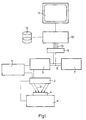
- FIG. 1 shows a schematic View more details of the pattern recognition system according to the invention. It is a programmable wafer tester 1 and a measuring probe device 2 assigned to it Measuring tips 3 as components of an automatic parametric Chip test system for measuring those manufactured on a wafer 4 DRAM memory chips provided. To the measuring device A large number of measuring instruments are connected 5 for recording and evaluating the electrical properties of the memory chips arranged on the wafer 4. To control the individual components of the measuring system a control processor 6 is provided, which for storage and pre-processing of the data associated with a fail memory 7 is.
- the control processor 6 of the measuring device communicates with the fail memory 7 via a data and address bus 8 which an interface card 9 is connected, via the the raw data from the fail memory 7 via lines 13 into one separate computer 10 can be read for further processing.
- the further processing of those read into the computer 10 Raw data is not done by algorhythmic as before Decomposing the measured failure patterns with conventional ones Programming technology, but more characteristic by extraction Characteristics from the dropout pattern and presentation of these characteristics as an input vector for a trained within the computer 10 neural network, which then the Classification of the entered failure pattern takes over how is explained in more detail below.
- the computer 10 is a display device such as associated with a screen 11 on which analyzed by means of the computer 10 Failure patterns and the result of the classification are displayed can be.
- the computer 10 also has a data memory 12 assigned to store the raw data and the processed data.
- Re 1 Measurement of the semiconductor chips of a wafer, processing the measured data, reading in the measured raw data, and processing the raw data for further analysis.
- measuring probe device 2 with Measuring tips 3 When measuring the chip failures by means of the measuring device consisting of the Prober 1, measuring probe device 2 with Measuring tips 3, measuring instruments 5, and processor 6 and fail Memory 7 are first of all semiconductor memory chips of the 6 "semiconductor wafer 2, the x and y coordinates of each individual chips on the wafer 2, as well as information about Current-voltage values of the chips (e.g. pass / fail information via an operation or stand-by current, generator voltages and the like) by means of the measuring device determined and for each chip the failure pattern and the Default rate, i.e. the percentage of total failure cells present measured.
- Current-voltage values of the chips e.g. pass / fail information via an operation or stand-by current, generator voltages and the like
- FIG. 2 shows a schematic Top view of a physical block 14 of a semiconductor memory chip with 256 word lines WL1 to WL256 and 1024 bit lines BL1 to BL1024.
- the memory cells of the Chips are each at the intersection of a word line WLn and a bit line BLm arranged.
- Figure 2 there are some typical ones Arrangements of faulty memory cells are shown.
- reference numerals 15, 16 denote 17 individually failed at the associated word-bit line crossing Single cells (single bit failures), the reference numbers 18 and 19 immediately adjacent falling single cells (pairwise bit failure), the reference numbers 20, 21, 22, 23 side by side failed on part of a word line Memory cells, with the word line failure 20 additionally another separate failure 24 with another Failure state than in the other failure cells
- Word line 20 is shown
- the reference numeral 25 denotes an accumulation of adjacent failure cells (so-called cluster)
- the reference number 26 a failure of several adjacent bit lines
- the one generated by the measuring device or the chip test system binary raw file with information for a wafer or at Block measurements for one lot, i.e. one due to production associated group of several identical wafers as a raw data file via lines 13 (see FIG. 1) in read the computer 10.
- header information such as lot number, wafer number and assigned Design type.
- a chip information consists of a chip info block, followed by 16 hexadecimal information (so with the 4 mega semiconductor chip) or 512 segment information (so with 16 mega semiconductor memory).
- the chip info block shows that the data for one follow a specific chip, namely the x and y coordinates the chip on the wafer, as well as technical information, for example information about current-voltage values of the chip.
- Hexadecimal information indicates that now the data for a new hexadecimal follows, namely the Hexadecimal number (with 4 mega semiconductor memory) or the Segment number (with 16 mega semiconductor memory), and there then a number of 256 word line counters or Column counters and 1024 bit line counters or line counters for total failure, and a corresponding number of coordinate counters for zero failures and one failures.
- the failure patterns of a chip were all x and y coordinates of the failure cells and the underlying Failure condition determined.
- each physical block 1 of the semiconductor chip a number of 256 line counters ZZ1 to ZZ256 and determined a number of 1024 column counters SZ1 to SZ1024, each of which is information alongside the number of the assigned row 1 to 256 or column 1 to 1024 the number the total occurring on this row or column Failure cells for each of the three failure states are included.
- the Coordinate counters thus give the projected onto the coordinate Total values of all failures with a certain failure condition (i.e. '0', '1', or '0' and '1') of the assigned Management again ("projection").
- the main global, i.e. related to an entire wafer Data structures are the following dynamically created Arrays. You can directly for the 4 mega semiconductor memory taken from the hexadecimal information of the raw data file be while for the 16 mega semiconductor memory from the segment information - modified accordingly - compiled become. Obtain the following explanations each on the 4 megabit chip, however, apply analogously also for a 16 megabit semiconductor memory. For customization of the analysis method according to the invention on chip generations larger or smaller 4 megabits are essentially required just changing some global constants that are defined in a predetermined program unit, and the adaptation of the program unit to generate the physical Blocks from the column and row counters of the raw data file.
- Echoes are only searched for if the corresponding one Hexadecant is not a total failure because then would have any failing word line and bit line projection in the other hexadecimal an echo, respectively if the respective failure patterns are not too chaotic Have character. Will a line in the corresponding Hexadecanals recognized as echo, so the line is off the central data structures and it will Flag signal flg [x, 5] of that line causing it for the echo is set to a value 'true'. In line elimination it should be taken into account that for example a failing bit line in the word line projection on each array element the line counter of the even one and odd hexadecimal edges projected with the value one becomes.
- the echo projection should not only be used in Bit line direction are eliminated, but it should be in the Echo hexadecants additionally the 256 projections with the Value one on the word line projection can be eliminated.
- a so-called baseline is the knowledge of the baseline widths in the elimination process requirement in both projection directions. The baseline widths are determined before each elimination. Lines are only eliminated up to the current one Baseline. The considerations made above to the echo problem are omitted if - conditionally, for example through the chip design - no echoes can occur, or consideration of echoes is not desired for other reasons or is required.
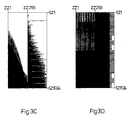
- FIGS. 3A to 3F "massive" failure pattern of a physical block shown, each figure consists of two halves, in the right half to the right the values of Column counters from SZ 1 to SZ 1024 to the right, and on the the left half of the screen shows the values of the line counters from ZZ 1 to ZZ 256 are plotted upwards.
- the typical shown Failure patterns represent part of the classes used to assess the failure mechanisms; indeed the number of such classes is typically around 70 or more.
- the actual sample classification is started.
- two different analysis methods used: a first neural network NN1 for analysis of a physical block with errors massive error, and a second neural network NN2 for the analysis of a faulty physical block regarding errors with low error mass.
- the usage different methods depending on the initially measured Failure rate is in terms of speed the analysis or optimization of the determined classification results performed. It should be taken into account that the use of a neural network in particular with large amounts of data the advantage of a considerably larger one Computing speed offers, however, with a considerable Loss of information is connected.
- the automatic pattern recognition process with conventional ones Methods a long computing time or high Occupancy rate of the computer is required, however, it can in turn more information will be obtained.
- step S1 all are first raw data obtained from the measuring device into the computer 10 entered and the failure rate FC ("Fail Count") of the ratio of the defective memory cells calculated for the total number. If the failure rate FC at step S2 is determined to be greater than about 99% in step S3 a total failure of the semiconductor chip is assumed and the process goes directly to a result section via branch 29 30 of the main program. If the default rate is FC at step S2 is determined to be less than 99%, branches the program to step S4, in which using the first neural network NN1 an analysis of the failure patterns and classification is carried out. If the classification succeeds, the method goes directly via branch 29 continue to section 30 of the main program.
- FC Failure Rate
- step S5 If a classification is not possible in step S5 is in a further branch a fine analysis again carried out; namely, an analysis and Classification of the failure pattern using a second neural network NN2 performed. If one The procedure is successful if the failure patterns are classified to section 30 of the main program in which the determined Category of the failure pattern is output. If a classification does not succeed, this becomes in step S7 determined and in section 30 a non-classifiable category spent.
- the first neural network NN1 decides on submission this input vector, what class of error the Failure acts or gives the failure for further processing free if there is no massive error class.
- First neural network NN1 is an arrangement of RCE type used, the principle of its operation is schematic based on a geometric interpretation according to the figures 5 and 6, and Figures 7A and 7B is explained.
- the neural network NN1 implemented in the computer 10 5 of the RCE type has three levels, one input level 31, a computing level 32, and an output level 33 Input level 31 has a number of 27 processing elements X1 to X27, each of which has a component E1 to E27 of the 27-dimensional input vector is assigned.
- the Processing elements X1 to X27 of the input level 31 is one Variety of processing elements Y1 to Ym of the computing level 32 assigned, the number m of processing elements Y of the computing level 32 is generally much larger as the dimension n of the input vector, and for example on the complexity of the calculation and classification of the analyzing dot pattern depends.
- At computing level 32 a 27-dimensional arrangement of not necessarily coherent spatial areas formed, the spatial form complex decision areas.
- FIG. 6 is a first component E1 of the right Input vector, and up a second component E2 of the Input vector plotted.
- E1 and E2 of the input vector Hyperspheres shown in two dimensions Case simply circles
- FIG. 6 are just two classes A and B for simplicity with the corresponding associated room areas schematically shown.
- circles or spatial areas 34, 35, 36, 37, 38 are shown, which are assigned to class A, and circles or spatial areas 39, 40, 41, 42, 43 that the Class B can be assigned.
- the arrangement of the room areas, i.e. their centers and their respective extent in Space taking into account the assignment to a specific Class is determined after training the neural network selected sample pattern.
- the Computing level 32 of the neural network NN1 is the one in the Input level 31 entered 27-dimensional input vector accordingly evaluates the arrangement of hyperspheres, related to a particular class, it belongs. If such Assignment to a certain class succeeds in the the output level 33 assigned to the computing level 32 accordingly determined class issued.
- the number of outputs Z1 and Z2 of the output level 33 corresponds essentially to that Number of classes specified. With the schematic explanation according to FIGS. 5 and 6, only two classes are A and B and correspondingly two output elements Z1 and Z2 of Output level 33 shown; in reality the number is of the classes or the number of output elements more than about 70.
- FIG. 7A shows the case in which the respective Classes A and B belonging to areas 44 and 45 of the Input vectors 46 and 47 do not overlap. In this case is a unique assignment of one at the input level 31 of the neural network to a test vector certain class A or B possible.
- figure shows 7B shows the case of two overlapping spatial areas 48 and 49; in this case, the neural training procedure Network within the computing level 32 which is the vector 50 and 51 orderly arranged room areas 48 and 49 to the extent i.e. to rejuvenate that there is no longer any overlap.
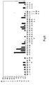
- the exam can be started any existing, special distributions of Error classes can be made over the entire wafer.
- One third neural network will be 22 different Distributions of failure patterns on the wafer that trained
- the following topographies can include: Accumulation defective chips over the entire edge of the wafer on which left or right edge of the wafer, accumulation defective Chips in the upper / lower and upper / lower lateral edge area of the wafer, accumulation of defective chips in the area of the Flat or anti-flat of the wafer, accumulation of faulty chips in a central ring area of the wafer, and the like.
- Distinctive distributions but not specially learned by the network from the third neural network with a Question marks classified. It is in the Usually either around particularly massive error classes over the entire wafer or around massive clustering of errors an error class, such as that caused by ill-treatment (Scratches) on the wafers.
- an error class such as that caused by ill-treatment (Scratches) on the wafers.
Abstract
Description
Die Erfindung bezieht sich auf eine Vorrichtung und ein Verfahren zur Erfassung und Bewertung eines in einem mehrdimensionalen Koordinatensystem angeordneten räumlich diskreten Punktmusters, wobei jeder Punkt des Musters wenigstens zwei unterscheidbare Zustandswerte annimmt. Insbesondere bezieht sich die Erfindung auf eine Vorrichtung und ein Verfahren zur Erkennung und Klassifizierung der binären Ausfallmuster von defekten Speicherzellen eines Halbleiterspeichers.The invention relates to an apparatus and a method to capture and evaluate one in a multidimensional Coordinate system arranged spatially discrete Dot pattern, each dot of the pattern being at least two distinguishable state values. In particular relates the invention relates to an apparatus and a method for Detection and classification of the binary failure patterns of defective memory cells of a semiconductor memory.
Die Ausfallmuster der Speicherzellen von defekten Halbleiterspeichern geben Hinweise auf die den Ausfällen zugrunde liegenden Technologieprobleme bei der Herstellung der Halbleiterspeicher. Neben der möglichen rein statistischen Verteilung der Ausfallmuster auf einem Wafer, die in der Regel auf Partikelprobleme bei bestimmten Prozessen der Chipherstellung schließen läßt, geben insbesondere nichtstatistische Verteilungen der Ausfallmuster auf einem Wafer nach Auswertung geeignete Hinweise auf systematische Technologie- und Prozeßprobleme. Um auf einer statistisch ausreichenden Basis Aussagen über solche Probleme treffen zu können, ist es notwendig, die Ausfallmuster einzelner Halbleiterchips bzw. Verteilungen der Ausfallmuster über einen gesamten Siliziumwafer zu erkennen und zu klassifizieren. Eine Schwierigkeit besteht hierbei unter anderem darin, daß Ausfallmuster in verschiedensten und immer neuen Varianten auftreten können. Weiterhin sind die der Analyse zugrundeliegenden, vermittels Chiptestsystemen gewonnenen Rohdatenmengen enorm. Bei einem dynamischen Halbleiterspeicherchip mit einer Speichergröße von beispielsweise 4 Mega fallen bei Berücksichtigung von ausfallenden reinen Null-Zellen, reinen Eins-Zellen und der Veroderung von Null- und Eins-Zellen im ungünstigsten Fall 4 Megabit • 3 = 12 Megabit an Rohdaten an. Hieraus ergibt sich eine Zahl der theoretisch denkbaren Varianten von Ausfallmustern bei einem 4-Megabit-Speicher von 24194301-1, eine Zahl mit rund 1,2 Millionen Stellen. Mit Hilfe von "Landkarten", sogenannten Bitmaps, welche Muster von nichtfunktionierenden Speicherzellen darstellen, wird versucht, diese nahezu unendlich große Zahl von Ausfallmustern zu ordnen. Obzwar aufgrund der Ähnlichkeit der gewonnenen Bitmaps eine Einteilung in etwa 80 bis 100 Ausfallklassen durchgeführt werden kann, werden bei einer manuellen Bewertung durch eine Bedienungsperson für die visuelle Fehleranalyse sämtlicher Ausfallmuster eines Wafers von typischerweise 6" Durchmesser etwa 15 Stunden benötigt. Es ist versucht worden, die Analyse der Ausfallmuster mit herkömmlichen Methoden durch einen Rechner zu automatisieren; die Ergebnisse stellten sich hingegen als äußerst unbefriedigend dar, da zum einen wichtige Fehlerklassen von Ausfallmustern rechnerisch nicht erfaßt werden und eine manuelle Nachbearbeitung durch einen geschulten Fachmann erfordern, und zum anderen die Analysezeiten bei den bisherigen Methoden auch unter Verwendung modernster Rechnermittel mit hohen Rechengeschwindigkeiten noch zu lang ausfallen, so daß eine Anwendung der bisher verwendeten Analyseverfahren namentlich auf größere Halbleiterspeicher mit 4 Mega und mehr wenig praktikabel ist. Bei dem bisher angewandten Verfahren wurden aufgrund der hohen Rechenzeit zur Analyse von Speicherchipausfallmustern einzelne Wafer bzw. Speicherchip-Bausteine der laufenden Produktion lediglich stichprobenweise entnommen und separat mit einem speziellen Analyseprogramm gemessen. Hierbei wurden nach einer Vorverarbeitung der Daten in einem speziell hierfür vorgesehenen Datenspeicher ("Fail Memory") der Meßvorrichtung die vorverarbeiteten Daten als Rohdatei von der Meßvorrichtung an einen Rechner übertragen und dort einer mit konventioneller Programmiertechnik erstellten Hauptanalyse unterzogen. Ein erheblicher Nachteil bestand bei dieser Vorgehensweise ferner darin, daß bei einem Übergang auf eine neue Speichergeneration erhebliche Teile der Vor- und Hauptanalyse neu programmiert werden mußten. Ebenso mußten neu zu analysierende Typen von Ausfallmustern mit großem Aufwand neu programmiert werden.The failure patterns of the memory cells of defective semiconductor memories provide information about the technology problems underlying the failures when manufacturing the semiconductor memories. In addition to the possible purely statistical distribution of the failure patterns on a wafer, which usually suggests particle problems in certain processes in chip manufacture, non-statistical distributions of the failure patterns on a wafer after evaluation give suitable indications of systematic technology and process problems. In order to be able to make statements about such problems on a statistically sufficient basis, it is necessary to recognize and classify the failure patterns of individual semiconductor chips or distributions of the failure patterns over an entire silicon wafer. One of the difficulties here is that failure patterns can occur in a wide variety of new variants. Furthermore, the raw data quantities on which the analysis is based and obtained using chip test systems are enormous. In the case of a dynamic semiconductor memory chip with a memory size of, for example, 4 mega, 4 megabits • 3 = 12 megabits of raw data are obtained in the worst case, taking into account the failing pure zero cells, pure one cells and the ORing of zero and one cells. This results in a number of the theoretically conceivable variants of failure patterns with a 4 megabit memory of 2 4194301 -1, a number with around 1.2 million digits. With the help of "maps", so-called bitmaps, which represent patterns of non-functioning memory cells, an attempt is made to order this almost infinitely large number of failure patterns. Although, due to the similarity of the bitmaps obtained, a division into approximately 80 to 100 failure classes can be carried out, manual evaluation by an operator takes approximately 15 hours for a visual error analysis of all failure patterns of a typically 6 "diameter wafer. Automate the analysis of the failure patterns using conventional methods using a computer; the results, on the other hand, proved to be extremely unsatisfactory because, on the one hand, important failure classes of failure patterns are not calculated and require manual reworking by a trained specialist, and on the other hand the analysis times the previous methods are still too long, even with the use of the most modern computer means with high computing speeds, so that an application of the analysis methods used hitherto, particularly to larger semiconductor memories with 4 mega and more, is not very practical In the method used hitherto, individual wafers or memory chip modules from the current production were only sampled due to the high computing time for the analysis of memory chip failure patterns and measured separately with a special analysis program. Here, after preprocessing the data in a specially provided data memory ("fail memory") of the measuring device, the preprocessed data were transmitted as a raw file from the measuring device to a computer and subjected to a main analysis created using conventional programming technology. A major disadvantage of this procedure was also that considerable parts of the preliminary and main analysis had to be reprogrammed when changing over to a new memory generation. Likewise, types of failure patterns that had to be analyzed had to be reprogrammed with great effort.
Aus EP-A-0 633 536 ist eine Vorrichtung zur Erfassung und Bewertung eines aus Testmessungen an einem Apparat gewonnenen Ausfallmusters seiner Komponenten bekannt, wobei diese Vorrichtung im einzelnen aufweist: eine Meßeinrichtung (1,2) zum Gewinnen und Speichern der Rohdaten; einen dem Speicher zugeordneten Rechner (3), in den die abgespeicherten Daten eingegeben werden, und in welchem ein Merkmalextraktor (features extraction) vorgesehen ist, der die Rohdaten nach bestimmten Merkmalen bearbeitet und das Ergebnis in einem Computing Vector ausgibt; ein dem Rechner zugeordnetes neuronales Netzwerk (4), in welches der Computing Vector als Eingabevektor eingegeben wird und welches durch Vergleichen des Eingabevektors mit Vorgabevektoren einen Ausgabevektor berechnet, und einen Klassifikationswert (diagnosis) des gemessenen Ausfallsmusters anhand des ermittelten Ausgabevektors zuordnet und ausgibt. Zur Arbeitsweise des Merkmalextraktors ist ausgeführt, daß er gemäß Hunderter von mathematischen Funktionen arbeiten könnte; eine Arbeitsweise als Koordinatenzähler ist jedoch nicht erwähnt.From EP-A-0 633 536 a device for detecting and evaluating one is Test measurements on an apparatus obtained from its failure pattern Components known, this device comprises in detail: a Measuring device (1,2) for obtaining and storing the raw data; one to Memory-assigned computer (3) in which the stored data are entered, and in which a feature extractor (features extraction) is provided, which processes the raw data according to certain characteristics and outputs the result in a computing vector; one assigned to the computer Neural network (4), in which the computing vector as an input vector is entered and which by comparing the input vector with Default vectors compute an output vector, and a classification value (diagnosis) of the measured failure pattern based on the determined Assigns and outputs output vector. How the feature extractor works is designed to work according to hundreds of mathematical functions could; an operation as a coordinate counter is not mentioned.
Der Erfindung liegt die Aufgabe zugrunde, eine Vorrichtung und ein Verfahren zur Erfassung und Bewertung eines räumlich diskreten Punktmusters wie insbesondere eines Ausfallmusters eines Halbleiterspeicherchips zur Verfügung zu stellen, welche bzw. welches auch bei einer erheblichen Anzahl von Punkten, insbesondere im Bereich von größer als 1 Mega, eine selbsttätig und mit hoher Zuverlässigkeit und Reproduzierbarkeit durchzuführende Analyse und Klassifizierung des Punktmusters mit brauchbaren Analysezeiten ermöglicht.The invention has for its object a device and a method for recording and evaluating a spatial discrete dot pattern, such as a failure pattern in particular to provide a semiconductor memory chip, which or which also with a considerable number of points, especially in the range of greater than 1 mega, one automatically and with high reliability and reproducibility analysis and classification of the dot pattern to be carried out with usable analysis times.
Diese Aufgabe wird durch eine Vorrichtung gemäß Anspruch 1
und ein Verfahren gemäß Anspruch 5 gelöst.This object is achieved by a device according to
Erfindungsgemäß ist vorgesehen, daß die Analyse des räumlich diskreten Punktmusters vermittels einem in einem Rechner implementierten neuronalen Netzwerk durchgeführt wird, dem ein n-dimensionaler Eingabevektor mit n Komponenten zur Analyse angeboten wird, und welches durch Vergleichen des Eingabevektors mit abgespeicherten, auf der Grundlage von Beispielpunktmustern gewonnenen Vorgabevektoren einen Ausgabevektor berechnet, der zur Klassifikation des Punktmusters einen Klassifikationswert des gemessenen Punktmusters anhand des ermittelten Ausgabevektors ausgibt.According to the invention it is provided that the analysis of the spatial discrete dot pattern by means of a implemented in a computer neural network is carried out, the one n-dimensional input vector with n components for analysis is offered, and which by comparing the input vector with saved, based on sample point patterns default vectors obtained an output vector computes one to classify the dot pattern Classification value of the measured dot pattern based on the outputs determined output vector.
Hierbei stellt das neuronale Netzwerk eine Anordnung von untereinander verknüpften Verarbeitungselementen dar, sogenannten Neuronen, welche in einer hierarchischen Struktur mit mehreren Ebenen angeordnet sind. Jedes Neuron kann einen oder mehrere Eingänge besitzen, und besitzt in der Regel nur einen Ausgang. Das vorzugsweise verwendete neuronale Netzwerk besteht aus drei unterschiedlichen Ebenen: eine dem Eingabevektor zugeordnete Eingabeebene, ein dem Ausgabevektor zugeordnete Ausgabeebene, und eine zwischen der Eingabeebene und der Ausgabeebene angeordnete, den Vorgabevektoren zugeordnete Rechenebene. Die Anzahl der Neuronen in der Berechnungsebene hängt hierbei unter anderem ab von der Komplexität des dem neuronalen Netzwerkes für die Erkennung präsentierten Punktmusters, der gewünschten Informationskapazität des Netzwerkes, der Anzahl und dem Ausmaß der Fähigkeiten des trainierten neuronalen Netzwerkes, unbekannte Muster zu bearbeiten, sowie der Anzahl von Iterationen, welche das neuronale Netzwerk in der Trainingsphase durchführt, um sämtliche gewünschten Netzwerkrichtungen und Basiswerte zur Verfügung zu stellen.Here, the neural network places an arrangement between one another linked processing elements, so-called Neurons, which are in a hierarchical structure are arranged on several levels. Every neuron can have one or have multiple inputs, and usually have only one Output. The preferred neural network is used from three different levels: one the input vector assigned input level, an assigned to the output vector Output level, and one between the input level and the Output level arranged computing level assigned to the default vectors. The number of neurons in the calculation level depends among other things on the complexity of the neural network for the detection of presented dot patterns, the desired information capacity of the network, the number and extent of the skills trained neural network to process unknown patterns, and the number of iterations that the neural network Performed in the training phase to achieve all of the desired To provide network directions and basic values.
Bei der Betriebsweise des neuronalen Netzwerkes werden zwei nacheinander durchzuführende Prozeduren unterschieden: Zum einen das Training auf der Grundlage von Beispielpunktmustern mit bekannten Ausgängen, und zum anderen die eigentliche Erkennungsprozedur von unbekannten Mustern.In the operation of the neural network, two A distinction is made between procedures to be carried out successively: the training based on sample point patterns with known outputs, and on the other hand the actual recognition procedure of unknown patterns.
Beim Training des neuronalen Netzwerkes werden diesem aufeinanderfolgend vorbestimmte Eingabedatenmuster präsentiert, die sogenannten Beispielpunktmuster. Die Werte der neuronalen Basiswerte in dem neuronalen Netzwerk werden hierbei derart eingestellt, daß der Ausgang des Netzwerkes für jedes einzelne Trainingsmuster wenigstens ungefähr mit einem gewünschten entsprechenden Netzwerkausgang (Zielvektor bzw. Ausgabevektor) für das entsprechende Muster übereinstimmt. Nach der Vervollständigung des Trainings werden sämtliche Basiswerte bei ihren aktuellen Werten fixiert.When the neural network is trained, it becomes successive presents predetermined input data patterns that so-called sample dot pattern. The values of the basic neuronal values in this way in the neural network set that the output of the network for each one Training pattern at least roughly with a desired one corresponding network output (target vector or output vector) for the corresponding pattern. After Completion of the training will be all basic values fixed at their current values.
Daran anschließend kann das neuronale Netzwerk im Prinzip zur Erkennung von unbekannten Mustern verwendet werden. Bei der Mustererkennung werden die aus den unbekannten Punktmustern durch algorithmische Vorverarbeitung gewonnenen Eingabevektoren aufeinanderfolgend an die Eingänge des Netzwerkes angelegt, und entsprechend resultierende Netzwerkantworten von den Ausgabeknoten ausgegeben. The neural network can then be used in principle for Detection of unknown patterns can be used. In the Pattern recognition becomes that from the unknown point patterns input vectors obtained by algorithmic preprocessing successively applied to the inputs of the network, and corresponding network responses from output the output node.
Bei einer bevorzugten Ausführung der Erfindung ist vorgesehen, daß das neuronale Netzwerk eine Anordnung vom Typ des Restricted Coulomb Energy-Netzwerkes aufweist. Der Name Restricted Coulomb Energy bezieht sich auf eine Energiefunktion auf der Grundlage eines elektrostatischen Potentiales. Die Bezeichnung RCE-Netzwerk ist markenrechtlich für die Firma Nestor geschützt, welches ein Unternehmen des Nobelpreisträgers L. N. Cooper ist. Ein neuronales Netzwerk vom RCE-Typ besitzt genau drei Ebenen, eine Eingabeebene("input layer"), eine Rechenebene ("hidden layer"), und eine Ausgabeebene ("output layer"). Die Rechenebene ist vollständig mit der Eingabeebene verbunden. Weiterhin ist die Ausgabeebene teilweise mit der Rechenebene verbunden. Der Grund hierfür liegt darin, daß unterschiedliche Arten von Verarbeitungselementen in den Rechen- und Ausgabeebenen verwendet werden. Im Vergleich zu neuronalen Netzwerken vom Kohonen-Typ oder Perzeptron-Typ arbeiten RCE-Netzwerke aufgrund ihrer einfacheren Anordnung sehr schnell und effizient. Das neuronale Netzwerk wird wie folgt trainiert. Zunächst wird bei diesem Typ der Eingabeebene des neuronalen Netzwerkes ein n-dimensionaler Eingabevektor, der aus einem Beispielpunktmuster einer bekannten Klasse durch Vorverarbeitung gewonnen wurde, präsentiert, wobei der Eingabevektor einen Zielpunkt in einem n-dimensionalen Raum darstellt. In der mit der Eingabeebene verknüpften Rechenebene des neuronalen RCE-Netzwerkes wird um den Zielpunkt jedes Eingabevektors ein n-dimensionaler Raumbereich (Hypersphäre oder Hyperquader) mit dem Zielpunkt des Eingabevektors als Mittelpunkt des n-dimensionalen Raumbereiches festgelegt, wobei das Volumen dieses Raumbereiches entsprechend der zuzuordnenden Klasse eingestellt wird. Sämtliche Raumpunkte innerhalb dieses n-dimensionalen Raumbereiches gehören somit zu der vorbestimmten, dem jeweiligen Beispielpunktmuster zugehörenden Klasse. Dieses Verfahren wird mit weiteren Eingabevektoren, die zu weiteren Klassen gehören, wiederholt. Nach der Präsentation dieser weiteren Eingabevektoren stellt das neuronale Netzwerk fest, ob ein zu einer bestimmten Klasse gehörender Eingabevektor innerhalb des Raumbereiches eines zu einer anderen Klasse gehörenden Eingabevektors liegt. Falls dies zutrifft, werden die entsprechenden Raumbereiche durch geometrische Anpassung bzw. Verjüngung soweit geändert, daß ein zu einer bestimmten Klasse gehörender Eingabevektor nicht innerhalb des Raumbereiches eines zu einer anderen Klasse gehörenden Eingabevektors zu liegen kommt, wobei es im übrigen durchaus möglich sein kann, daß sich einige der Raumbereiche, auch solche unterschiedlicher Klassen, bereichsweise überlappen. Vorzugsweise werden zur Ausbildung der n-dimensionalen Raumbereiche Hyperquader verwendet, was im Gegensatz zur Verwendung von Hypersphären als Raumbereiche einer bestimmten Klasse den Vorteil besitzt, daß im Falle einer Anpassung der Raumbereiche nicht jede Dimension verjüngt werden muß. Im Falle der Verwendung von Hypersphären ist die Volumenabnahme des Raumbereiches bei einer Verjüngung stets größer als bei Hyperquadern. Damit ist die Möglichkeit der Verallgemeinerung, welche eine wichtige Eigenschaft von neuronalen Netzwerken darstellt, ungünstiger als im Falle von Quadern.In a preferred embodiment of the invention, that the neural network is a type Restricted Coulomb Energy network. The name Restricted Coulomb Energy refers to an energy function based on an electrostatic potential. The The RCE network is a trademark of the company Nestor protected, which is a Nobel Prize winner company L.N. Cooper is. An RCE-type neural network has exactly three levels, an input layer a computing level ("hidden layer"), and an output level ("output layer"). The computing level is complete with the Input level connected. Furthermore, the output level is partial connected to the computing level. The reason for this is in that different types of processing elements be used in the computing and output levels. Compared to Kohonen-type or perceptron-type neural networks RCE networks work because of their simpler Arrangement very quickly and efficiently. The neural network is trained as follows. First of all, this type of Input level of the neural network is an n-dimensional Input vector made from a sample point pattern of a known one Class obtained by preprocessing, presented, where the input vector is a target point in an n-dimensional Represents space. In the with the input level linked computing level of the neural RCE network is around the target point of each input vector is an n-dimensional space (Hypersphere or hypercube) with the target point of the Input vector as the center of the n-dimensional space fixed, with the volume of this room area accordingly the class to be assigned. All Spaces within this n-dimensional area thus belong to the predetermined, the respective sample point pattern belonging class. This procedure comes with other input vectors belonging to other classes, repeated. After presenting these other input vectors the neural network determines whether one is related to a particular one Class-related input vector within the space an input vector belonging to another class lies. If this is the case, the corresponding Spaces through geometric adjustment or tapering so far changed that one belonging to a certain class Input vector not within one to one space input class belonging to another class, although it may well be the case that some the room areas, including those of different classes, overlap in areas. Preferably be used for training of the n-dimensional spatial areas Hyperquader uses what in contrast to using hyperspheres as spatial areas a certain class has the advantage that in the case of a Adapting the room areas not tapering every dimension must become. In the case of using hyperspheres, the Volume decrease in the area always with a taper larger than with Hyperquadern. So that is the possibility of Generalization, which is an important property of neural Networks represents less favorable than in the case of Cuboids.
Ein Vorteil von RCE-Netzwerken besteht weiterhin allgemein darin, daß diese automatisch während der Trainingsprozedur konfiguriert werden. Die Trainingsprozedur kombiniert die Konfiguration und das Lernen durch die Verwendung des führenden Algorithmus. Demzufolge wird die Anzahl der Recheneinheiten ("Hidden units") in der Rechenebene des neuronalen Netzwerkes automatisch festgelegt. Neben der Festlegung von neuen Beispielmustern kann durch die Trainingsprozedur die Größe bzw. Ausdehnung der Raumbereiche einfacher angepaßt werden.An advantage of RCE networks continues to exist in general in that this automatically occurs during the training procedure can be configured. The training procedure combines the Configuration and learning through the use of the leading Algorithm. As a result, the number of processing units ("Hidden units") in the computing level of the neural network automatically set. In addition to setting new ones Sample sizes can be sized through the training procedure or expansion of the room areas can be adjusted more easily.
Ein wesentliches Merkmal der Erfindung besteht darin, daß dem neuronalen Netz nicht die ursprünglichen, physikalisch gemessenen Koordinaten- und Zustandswerte jedes Punktes des mehrdimensionalen räumlichen Punktmusters angeboten werden, sondern es werden zunächst Koordinatenzähler bzw. Koordinatenprojektionen für jeden Koordinatenwert einer Koordinatenachse aus den ursprünglichen Daten berechnet, wobei der Wert des Koordinatenzählers aus der Anzahl der erfaßten Punkte des Punktmusters der entsprechenden Koordinate mit einem vorbestimmten Zustandswert berechnet wird. Die eigentliche Mustererkennung vermittels des neuronalen Netzes findet auf der Grundlage der ermittelten Koordinatenzähler statt. Auf diese Weise werden die bei der Aufzeichnung der Koordinatenwerte und Zustandswerte jedes Punktes vermittels der Meßeinrichtung anfallenden Rohdatenmengen erheblich komprimiert. Beispielsweise ergibt sich bei der Analyse der Ausfallmuster eines Halbleiterchips vom 4 Megabit-Typ anstelle der Rohdatenanzahl von 4 Megabit • 3 = 12 Megabit nurmehr eine Datenmenge von (1024 + 256) • 3 • 16 Datenworte zu 16 Bit, also knapp 1 Megabit. Somit wird bei diesem Beispiel nur der zwölfte Teil der Datenmenge im Vergleich zu einer vollständigen Übertragung der Punktmusterdaten von der Meßeinrichtung zum Rechner übertragen. Diese Reduktion der Datenmenge ist allerdings mit einem Verlust an Information verbunden, der insbesondere dann auftritt, wenn sich mehr als ein Zustandswert einer Koordinate, beispielsweise ein einzelner Punktdefekt (im Falle eines Halbleiterspeichers ein elektrischer Ausfall, bei dem sowohl die x- als auch die y-Koordinate im Prinzip bekannt ist) innerhalb eines bestimmten Bereiches des Punktmusters befindet. In solchen Fällen ist zwar der Fehlertypus (beispielsweise Wort-Bit-Leitungs-Kreuzung, Einzelbit, Cluster usw.) in der Regel eindeutig ermittelbar, jedoch nicht die genaue x- und y-Koordinate im physikalischen Block des Halbleiterspeichers. Bei Ausfällen, die entweder nur wort- oder nur bitleitungsorientiert sind, tritt dieses Problem allerdings nicht auf.An essential feature of the invention is that neural network not the original, physically measured Coordinate and state values of each point of the multi-dimensional spatial dot pattern are offered, but first of all there are coordinate counters or coordinate projections for each coordinate value of a coordinate axis calculated from the original data, the value of the Coordinate counter from the number of points recorded Dot pattern of the corresponding coordinate with a predetermined one State value is calculated. The actual pattern recognition by means of the neural network takes place on the Basis of the determined coordinate counter instead. To this Ways become when recording the coordinate values and state values of each point by means of the measuring device resulting raw data quantities compressed considerably. For example the analysis of the failure patterns results in a 4 megabit-type semiconductor chips instead of the raw data count of 4 megabits • 3 = 12 megabits only a data amount of (1024 + 256) • 3 • 16 data words of 16 bits, ie almost 1 megabit. So in this example only the twelfth part the amount of data compared to a full transfer the dot pattern data from the measuring device to the computer transfer. This reduction in the amount of data is however with a loss of information, especially then occurs when there is more than one state value of a coordinate, for example a single point defect (in the case of a Semiconductor memory is an electrical failure in which both the x and y coordinates are known in principle) within of a certain area of the dot pattern. In such cases, the type of error (for example Word-bit line intersection, single bit, cluster, etc.) in the Usually clearly determinable, but not the exact x- and y coordinate in the physical block of the semiconductor memory. In the event of failures that are either only word-oriented or only bit line-oriented this problem does not occur.
Dem Prinzip der Erfindung folgend werden zur weiteren Reduktion der Datenmenge dem neuronalen Netzwerk nicht etwa die Koordinatenzähler unmittelbar als Eingabevektoren präsentiert, sondern ein n-dimensionaler Eingabevektor, wobei die Anzahl n typischerweise in der Größenordnung von etwa 10 bis etwa 30 liegt, bei dem die n Komponenten des Eingabevektors durch eine Reihe von Unterprozeduren aus den Werten der Koordinatenzähler des räumlich diskreten Punktmusters gewonnen werden.Following the principle of the invention for further reduction the amount of data the neural network does not have Coordinate counter presented directly as input vectors, but an n-dimensional input vector, the Number n typically on the order of about 10 to is about 30 where the n components of the input vector through a series of sub-procedures from the values of the coordinate counters of the spatially discrete dot pattern become.
Insbesondere können den Komponenten des n-dimensionalen Eingabevektors folgende numerische Werte, die unmittelbar aus den Koordinatenzählern des räumlich diskreten Punktmusters abgeleitet sind, zugeordnet werden:
- eine Abweichung vom Schwerpunkt der Koordinatenzähler des räumlich diskreten Punktmusters von Punkten mit einem vorbestimmten Zustandswert in Richtung einer bestimmten Koordinatenachse, und/oder
- eine Maßzahl für eine globale monotone Verteilung von Teilbereichen des Punktmusters von Punkten mit einem vorbestimmten Zustandswert, und/oder
- eine Maßzahl für die Periodizität des Punktmusters von Punkten mit einem vorbestimmten Zustandswert, und/oder
- ein zweites Moment der Massenverteilung von Punkten des Punktmusters mit einem vorbestimmten Zustandswert, und/oder
- einen Anteil von Koordinatenzählern mit mehr als einer vorbestimmten Anzahl von Punkten des Punktmusters mit einem vorbestimmten Zustandswert, und/oder
- einen Anteil von Echopunkten von Punkten des Punktmusters mit einem vorbestimmten Zustandswert, und/oder
- eine Maßzahl der Fluktuationen von Punkten benachbarter Koordinatenzähler des Punktmusters mit einem vorbestimmten Zustandswert, und/oder
- einen Anteil von Koordinaten mit weniger als eine vorbestimmte Anzahl der entsprechenden Koordinate von Punkten des Punktmusters mit einem vorbestimmten Zustandswert, und/oder
- eine Äquidistanz von Punkten des Punktmusters mit einem vorbestimmten Zustandswert in einem periodischen Teilbereich des Punktmusters, und/oder
- eine Anzahl von zusammenhängenden oder wenigstens teilweise zusammenhängenden Teilbereichen von Punkten des Punktmusters mit einem vorbestimmten Zustandswert in vorbestimmten Koordinatenrichtungen.
- a deviation from the center of gravity of the coordinate counter of the spatially discrete point pattern of points with a predetermined state value in the direction of a specific coordinate axis, and / or
- a measure for a global monotonous distribution of subregions of the point pattern of points with a predetermined state value, and / or
- a measure for the periodicity of the point pattern of points with a predetermined state value, and / or
- a second moment of the mass distribution of points of the point pattern with a predetermined state value, and / or
- a proportion of coordinate counters with more than a predetermined number of points of the point pattern with a predetermined state value, and / or
- a proportion of echo points from points of the point pattern with a predetermined state value, and / or
- a measure of the fluctuations of points of adjacent coordinate counters of the point pattern with a predetermined state value, and / or
- a proportion of coordinates with less than a predetermined number of the corresponding coordinate of points of the point pattern with a predetermined state value, and / or
- an equidistance of points of the point pattern with a predetermined state value in a periodic partial area of the point pattern, and / or
- a number of contiguous or at least partially contiguous partial areas of points of the point pattern with a predetermined state value in predetermined coordinate directions.
Hierbei kann in vorteilhafter Weise vorgesehen sein, daß die den n Komponenten des n-dimensionalen Eingabevektors zugeordneten numerischen Werte normiert sind, insbesondere in dem numerischen Zahlenbereich zwischen -1 und +1.It can advantageously be provided that the assigned to the n components of the n-dimensional input vector numerical values are standardized, especially in the numerical range between -1 and +1.
Bei einer besonders bevorzugten Ausführung der Erfindung ist vorgesehen, daß das mehrdimensionale Koordinatensystem des räumlich diskreten Punktmusters orthogonale Koordinatenachsen, insbesondere zwei orthogonale Koordinatenachsen aufweist, und der Wert jedes Koordinatenzählers durch Aufsummierung der erfaßten Punkte jeder Koordinate mit einem vorbestimmten Zustandswert und Projektion auf die entsprechende orthogonale Koordinatenachse, insbesondere Spaltenachse und Reihenachse gebildet wird.In a particularly preferred embodiment of the invention provided that the multi-dimensional coordinate system of the spatially discrete point pattern orthogonal coordinate axes, in particular has two orthogonal coordinate axes, and the value of each coordinate counter by adding up the detected points of each coordinate with a predetermined one Condition value and projection onto the corresponding one orthogonal coordinate axis, in particular column axis and Row axis is formed.
Bei einer besonders bevorzugten Anwendung der Erfindung ist vorgesehen, daß das Punktmuster das Ausfallmuster eines physikalisch zusammenhängenden Blockes von Speicherzellen eines Halbleiterspeichers aus einer Vielzahl auf der Hauptoberfläche eines Halbleiterwafers ausgebildeten Halbleiterspeichern darstellt. Hierbei besitzt jede Ausfallzelle des Ausfallmusters einen von drei Zustandswerten von denen ein Zustandswert einem Null-Ausfall der Speicherzelle, ein Zustandswert einem Eins-Ausfall der Speicherzelle und ein Zustandswert einem Null- und Eins-Ausfall der Speicherzelle zugeordnet ist. Hierbei sind die Speicherzellen des auf der Hauptoberfläche des Halbleiterwafers ausgebildeten Halbleiterspeichers in Bitleitungen bzw. Spalten und in Reihen bzw. Wortleitungen matrixförmig angeordnet, und die Koordinatenzähler stellen jeweils einen Spaltenzähler und einen Reihenzähler dar.In a particularly preferred application of the invention provided that the dot pattern is the failure pattern of a physical contiguous block of memory cells Semiconductor memory from a variety on the main surface of a semiconductor wafer formed semiconductor memories represents. Each failure cell has the failure pattern one of three state values, one of which is a state value a zero failure of the memory cell, a state value a one failure of the memory cell and a state value one Zero and one failure of the memory cell is assigned. Here, the memory cells are on the main surface of the semiconductor wafer formed semiconductor memory in Bit lines or columns and in rows or word lines Arranged in a matrix, and set the coordinate counters each represent a column counter and a row counter.
Von besonderem Vorteil werden bei dieser bevorzugten Anwendung der Erfindung den Komponenten des n-dimensionalen Eingabevektors folgende numerischen Werte zugeordnet:
- eine Abweichung vom Schwerpunkt von Ausfallzellen eines physikalischen Blockes des Halbleiterspeichers mit einem vorbestimmten Ausfallzustand in Bitleitungs- und/oder Wortleitungsrichtung; und/oder
- ein zweites Moment der Massenverteilung von Ausfallzellen eines physikalischen Blockes des Halbleiterspeichers mit einem vorbestimmten Ausfallzustand in Bitleitungs- und/oder Wortleitungsrichtung; und/oder
- eine Maßzahl der globalen monotonen Verteilung von Ausfallzellen eines physikalischen Blockes des Halbleiterspeichers mit einem vorbestimmten Ausfallzustand; und/oder
- eine Maßzahl für die Periodizität des Ausfallmusters von Ausfallzellen eines physikalischen Blockes des Halbleiterspeichers mit einem vorbestimmten Ausfallzustand, und/oder
- einen Anteil der Bitleitungen und/oder Wortleitungen von
Ausfallzellen eines physikalischen Blockes des Halbleiterspeichers
mit einem vorbestimmten Ausfallzustand mit mehr als
einem vorgegebenen ersten Grenzwert auf der betroffenen Leitung;
und/oder
- einen Anteil von Bitleitungen und/oder Wortleitungen von Ausfallzellen eines physikalischen Blockes des Halbleiterspeichers mit einem vorbestimmten Ausfallzustand mit mehr als einem vorgegebenen zweiten Grenzwert auf der betroffenen Leitung, wobei die betroffenen Wort- und/oder Bitleitungen ein Echo in benachbarten physikalischen Blöcken aufweisen; und/oder
- eine Maßzahl für die Fluktuationen von Ausfallzellen eines physikalischen Blockes des Halbleiterspeichers mit einem vorbestimmten Ausfallzustand zwischen benachbarten Bitleitungen und/oder benachbarten Wortleitungen; und/oder
- einen Anteil von Bitleitungen und/oder Wortleitungen mit Ausfallzellen eines physikalischen Blockes des Halbleiterspeichers mit einem vorbestimmten Ausfallzustand mit weniger als einem dritten Grenzwert von Ausfallbits auf der betroffenen Wort- und/oder Bitleitung; und/oder
- eine Maßzahl für die Äquidistanz ausfallbehafteter Bitleitungen und/oder Wortleitungen mit einem periodischen Muster;
- eine Maßzahl für die Anzahl von größeren Gruppen von Ausfallzellen in Bitleitungs- und/oder Wortleitungsrichtung; und/oder
- einen Anteil von Bitleitungen und/oder Wortleitungen, welche Zwischenschichtkurzschlüsse in Bit- und/oder Wortleitungsrichtung aufweisen; und/oder
- die Gesamtzahl von Ausfallzellen; und/oder
- eine Maßzahl für am Randbereich des Wafers gehäuft auftretende Ausfallzellen; und/oder
- ein Verhältnis zwischen längeren ausfallbedingten Wort-und/oder Bitleitungen in Wortleitungs- und/oder Bitleitungsrichtung.
- a deviation from the center of gravity of failure cells of a physical block of the semiconductor memory with a predetermined failure state in the bit line and / or word line direction; and or
- a second moment of the mass distribution of failure cells of a physical block of the semiconductor memory with a predetermined failure state in the bit line and / or word line direction; and or
- a measure of the global monotonic distribution of failure cells of a physical block of the semiconductor memory with a predetermined failure state; and or
- a measure for the periodicity of the failure pattern of failure cells of a physical block of the semiconductor memory with a predetermined failure state, and / or
- a proportion of the bit lines and / or word lines of failure cells of a physical block of the semiconductor memory with a predetermined failure state with more than a predetermined first limit value on the line concerned; and or
- a proportion of bit lines and / or word lines from failure cells of a physical block of the semiconductor memory with a predetermined failure state with more than a predetermined second limit value on the affected line, the affected word and / or bit lines having an echo in adjacent physical blocks; and or
- a measure for the fluctuations of failure cells of a physical block of the semiconductor memory with a predetermined failure state between adjacent bit lines and / or adjacent word lines; and or
- a proportion of bit lines and / or word lines with failure cells of a physical block of the semiconductor memory with a predetermined failure state with less than a third limit value of failure bits on the affected word and / or bit line; and or
- a measure of the equidistance of failing bit lines and / or word lines with a periodic pattern;
- a measure of the number of larger groups of failure cells in the bit line and / or word line direction; and or
- a proportion of bit lines and / or word lines which have interlayer short-circuits in the bit and / or word line direction; and or
- the total number of failure cells; and or
- a measure of failure cells that occur frequently at the edge region of the wafer; and or
- a relationship between longer failure-related word and / or bit lines in the word line and / or bit line direction.
Die Erfindung ermöglicht durch den Einsatz eines neuronalen Netzwerkes eine zuverlässige Klassifikation von SpeicherchipAusfallmustern, welche auch parallel neben dem üblichen Funktionstest von Speicherchips während einer Standardproduktionsmessung durchgeführt werden kann. Der Vorverarbeitungsalgorhythmus zur Bereitstellung der Eingabedaten für das neuronale Netzwerk und das neuronale Netzwerk selbst sind skalierbar und ermöglicht damit den Einsatz der verwendeten Software bei einem Übergang von einer Chipgeneration zur nächsten, ohne daß diese neu programmiert werden müßte. Darüber hinaus können qualitativ neu auftretende Ausfallmuster durch einfaches Training, d.h. Lernen anhand eines Beispielmusters, auf einfache Weise berücksichtigt werden, ohne daß eine Änderung des im Rechner ablaufenden Programmes erforderlich ist. Zur Implementierung des Analyseprogramms kann ein kostengünstiger Rechner, beispielsweise ein handelsüblicher Personal Computer (PC) verwendet werden, der beispielsweise über eine Schnittstellenkarte mit dem Rechner bzw. dem Mikroprozessor des Chiptestsystems verbunden ist. Damit ist es auch möglich, durch paralleles Herausführen des Daten- und Adressbussystems, über welches der Mikroprozessor des Chiptestsystems mit dem Fail Memory des Testsystems kommuniziert, auf die Schnittstellenkarte des PC's das Ausfallmuster im Fail Memory parallel zu dessen Verarbeitung im Chiptestsystem in den separat angeordneten PC einzulesen und dort weiterzuverarbeiten. Im Gegensatz zur konventionellen Ausfallmusteranalyse erfolgt die Weiterverarbeitung hierbei nicht wie bisher durch algorhythmisches Zerlegen der Ausfallmuster mit konventioneller Programmiertechnik, sondern durch Extraktion charakteristischer Merkmale aus dem Ausfallmuster und Vorlage dieser Merkmale als Eingabevektor für ein neuronales Netzwerk, welches dann die Klassifizierung der Ausfallmuster übernimmt. Die Erfindung bietet hierbei auch den Vorteil, die eigentliche Mustererkennungsaufgabe nicht auf sehr teueren ChipTestsystemen durchzuführen, sondern auf im Vergleich dazu sehr kostengünstiger PC-Hardware. Demgegenüber können erfindungsgemäß die Chip-Testsysteme bzw. die Meßeinrichtung ausschließlich zur schnellen Rohdatenerfassung eingesetzt werden.The invention enables through the use of a neural Network a reliable classification of memory chip failure patterns, which also parallel to the usual function test memory chips during a standard production measurement can be carried out. The preprocessing algorithm to provide the input data for the neural Network and the neural network itself are scalable and thus enables the use of the software used with a transition from one chip generation to the next, without that this would have to be reprogrammed. Furthermore can newly emerging failure patterns by simple Training, i.e. Learn based on a sample simple way to be taken into account without making a change of the program running in the computer is required. For Implementing the analysis program can be an inexpensive Computer, for example a commercially available personal computer (PC) can be used, for example, via an interface card with the computer or the microprocessor of the Chip test system is connected. It is also possible by bringing out the data and address bus system in parallel, via which the microprocessor of the chip test system communicates with the fail memory of the test system to which Interface card of the PC's failure pattern in the fail memory parallel to its processing in the chip test system in the separate read in the arranged PC and process it there. In contrast to conventional failure pattern analysis Further processing is not carried out here as before algorithmic decomposition of the failure patterns with conventional Programming technology, but more characteristic by extraction Characteristics from the failure pattern and presentation of this Features as an input vector for a neural network, which then the classification of the failure patterns takes over. The invention also offers the advantage of being the actual one Pattern recognition task not on very expensive chip test systems perform but on compared to that very inexpensive PC hardware. In contrast, according to the invention the chip test systems or the measuring device exclusively can be used for fast raw data acquisition.
Weitere Merkmale, Vorteile und Zweckmäßigkeiten der Erfindung ergeben sich aus der Beschreibung eines bevorzugten Ausführungsbeispieles anhand der Zeichnung. Es zeigt:
Figur 1- eine schematische Darstellung der erfindungsgemäßen Vorrichtung gemäß einem Ausführungsbeispiel;
Figur 2- eine schematische Ansicht von Ausfallzellen in Draufsicht eines auf der Hauptoberfläche eines Siliziumwafers ausgebildeten Halbleiterspeichers, bei dem die Speicherzellen in Bitleitungen und Wortleitungen matrixförmig angeordnet sind;
- Figuren 3A bis 3F
- schematische Ansichten der Koordinatenzähler von typischerweise vorkommenden Ausfallmustern der Speicherzellen eines physikalischen Blockes, wobei jeweils auf der rechten Teilansicht der Figuren die Bitleitungszähler, und auf der linken Teilansicht die Wortleitungszähler aufgetragen sind;
Figur 4- ein Flußdiagramm zur Erläuterung des Verfahrensablaufes eines bevorzugten Ausführungsbeispieles der Erfindung;
Figur 5- eine schematische Ansicht eines RCE-Netzwerkes mit
drei Netzwerkebenen;
Figur 6 eine Darstellung zur Erläuterung der prinzipiellen Arbeitsweise eines RCE-Netzwerkes anhand einer geometrischen Interpretation; - Figur 7A und 7B
- schematische Darstellungen zweier zweidimensionaler Eingabevektoren, wobei bei der Teilansicht 7A der erste Vektor nicht innerhalb des Raumbereiches des zweiten Vektors liegt, und bei der Teilansicht 7B der erste Vektor innerhalb des Raumbereiches des zweiten Vektors liegt und demzufolge eine Verjüngung wenigstens eines Raumbereiches erforderlich ist;
Figur 8- ein schematisches Balkendiagramm als Ergebnis einer Bewertung von auf einem Wafer vorkommenden Klassen von Ausfallmustern.
- Figure 1
- a schematic representation of the device according to the invention according to an embodiment;
- Figure 2
- a schematic view of failure cells in plan view of a semiconductor memory formed on the main surface of a silicon wafer, in which the memory cells are arranged in a matrix in bit lines and word lines;
- Figures 3A to 3F
- schematic views of the coordinate counters of typically occurring failure patterns of the memory cells of a physical block, the bit line counters being plotted on the right partial view of the figures and the word line counters being plotted on the left partial view;
- Figure 4
- a flowchart to explain the process flow of a preferred embodiment of the invention;
- Figure 5
- a schematic view of an RCE network with three network levels; FIG. 6 shows an illustration to explain the basic mode of operation of an RCE network on the basis of a geometric interpretation;
- Figure 7A and 7B
- schematic representations of two two-dimensional input vectors, wherein the partial view 7A, the first vector is not within the spatial area of the second vector, and the partial view 7B, the first vector lies within the spatial area of the second vector and consequently a tapering of at least one spatial area is required;
- Figure 8
- a schematic bar diagram as a result of an evaluation of classes of failure patterns occurring on a wafer.
In den Figuren ist ein bevorzugtes Ausführungsbeispiel der
Erfindung dargestellt, bei dem die Ausfallmuster der Speicherzellen
eines defekten dynamischen Halbleiterspeichers vom
Typ 4 Mega untersucht werden. Selbstverständlich ist die Erfindung
ohne weiteres zur Analyse von größeren Halbleiterspeichern,
beispielsweise 16 Mega, 256 Mega und mehr möglich;
auf soweit erforderliche Besonderheiten wird an einigen Stellen
der nachfolgenden Beschreibung gesondert eingegangen.In the figures, a preferred embodiment is the
Invention shown, in which the failure pattern of the memory cells
a defective dynamic semiconductor memory from
Das dargestellte Ausführungsbeispiel entspricht einem automatisierten
Mustererkennungssystem, wie es in der Megabit-Chipfertigung
eingesetzt wird. Figur 1 zeigt in einer schematischen
Ansicht nähere Einzelheiten des Mustererkennungssystems
gemäß Erfindung. Es ist ein programmierbarer Waferprober
1 und eine diesem zugeordnete Messondeneinrichtung 2 mit
Messpitzen 3 als Bestandteile eines automatischen parametrischen
Chiptestsystems zur Messung der auf einem Wafer 4 gefertigten
DRAM-Speicherbausteine vorgesehen. An die Messeinrichtung
angeschlossen sind eine Vielzahl von Messinstrumenten
5 zur Erfassung und Auswertung der elektrischen Eigenschaften
der auf dem Wafer 4 angeordneten Speicherbausteine.
Zur Steuerung der einzelnen Bestandteile der Messeinrichtung
ist ein Steuerprozessor 6 vorgesehen, dem zur Abspeicherung
und Vorverarbeitung der Daten ein Fail Memory 7 zugeordnet
ist. Der Steuerprozessor 6 der Meßeinrichtung kommuniziert
mit dem Fail Memory 7 über einen Daten- und Adressbus 8, an
den eine Schnittstellenkarte 9 angeschlossen ist, über die
die Rohdaten aus dem Fail Memory 7 über Leitungen 13 in einen
separaten Rechner 10 zur Weiterverarbeitung eingelesen werden.
Die Weiterverarbeitung der in den Rechner 10 eingelesenen
Rohdaten erfolgt nicht wie bisher durch algorhythmisches
Zerlegen der gemessenen Ausfallmuster mit konventioneller
Programmiertechnik, sondern durch Extraktion charakteristischer
Merkmale aus dem Ausfallmuster und Vorlage dieser Merkmale
als Eingabevektor für ein innerhalb des Rechners 10 ausgebildetes
neuronales Netzwerk, welches anschließend die
Klassifizierung der eingegebenen Ausfallmuster übernimmt, wie
nachstehend näher erläutert wird. Dem Rechner 10 ist eine Anzeigeeinrichtung
wie beispielsweise ein Bildschirm 11 zugeordnet,
auf dem das vermittels des Rechners 10 analysierte
Ausfallmuster und das Ergebnis der Klassifikation angezeigt
werden kann. Dem Rechner 10 ist ferner ein Datenspeicher 12
zur Ablage der Rohdaten und der verarbeiteten Daten zugeordnet.The illustrated embodiment corresponds to an automated one
Pattern recognition system such as that used in megabit chip production
is used. Figure 1 shows a schematic
View more details of the pattern recognition system
according to the invention. It is a
Das Verfahren gemäß Ausführungsbeispiel kann grob in vier
Funktionseinheiten unterteilt werden:
Im folgenden werden die vier Funktionseinheiten näher erläutert.The four functional units are explained in more detail below.
Zu 1. Messung der Halbleiterchips eines Wafers, Verarbeitung
der Meßdaten, Einlesen der gemessenen Rohdaten, und Aufbereiten
der Rohdaten zur weiteren Analyse.
Bei der Messung der Chipausfälle vermittels der Meßeinrichtung
bestehend aus dem Prober 1, Meßsondeneinrichtung 2 mit
Meßspitzen 3, Meßinstrumenten 5, sowie Prozessor 6 und Fail
Memory 7 werden zunächst von sämtlichen Halbleiterspeicherchips
des 6"-Halbleiterwafers 2 die x- und y-Koordinaten jedes
einzelnen Chips auf dem Wafer 2, sowie Informationen über
Strom-Spannungswerte der Chips (beispielsweise Pass/Fail-Information
über einen Operations- bzw. Stand-by-Strom, Generatorspannungen
und dergleichen) vermittels der Meßeinrichtung
bestimmt und für jeden Chip das Ausfallmuster und die
Ausfallquote, d.h. der Anteil der insgesamt vorhandenen Ausfallzellen
gemessen. Bereits bei der Messung bzw. Voranalyse
der Ausfallmuster eines Halbleiterchips vermittels der
Meßeinrichtung wird jeder Chip in physikalisch zusammenhängende
Blöcke, welche beim 4 Mega-Speicher auch als Hexadekanten
bezeichnet werden, unterteilt, so daß die eigentliche Musteranalyse
in dieser physikalischen Untereinheit durchgeführt
wird. Somit erfolgt die Analyse beim 4 Megabit-Speicherchip
hexadekantenweise. Figur 2 zeigt eine schematische
Draufsicht eines physikalischen Blockes 14 eines Halbleiterspeicherchips
mit 256 Wortleitungen WL1 bis WL256 und
1024 Bitleitungen BL1 bis BL1024. Die Speicherzellen der
Chips sind hierbei jeweils an Kreuzungsstellen einer Wortleitung
WLn und einer Bitleitung BLm angeordnet. Ein physikalischer
Block 14 besitzt somit eine Anzahl von 256 • 1024 =
262 144 Speicherzellen. In Figur 2 sind einige typisch vorkommende
Anordnungen von fehlerhaften Speicherzellen dargestellt.
Beispielsweise bezeichnen die Bezugsziffern 15, 16,
17 an der zugehörenden Wort-Bit-Leitungskreuzung einzeln ausgefallene
Einzelzellen (Einzelbitausfälle), die Bezugsziffern
18 und 19 unmittelbar benachbart liegende ausfallende Einzelzellen
(paarweiser Bitausfall), die Bezugsziffern 20, 21, 22,
23 nebeneinander auf einem Teil einer Wortleitung ausgefallene
Speicherzellen, wobei bei dem Wortleitungsausfall 20 zusätzlich
noch ein gesonderter Einzelausfall 24 mit einem anderen
Ausfallzustand als bei den übrigen Ausfallzellen dieser
Wortleitung 20 dargestellt ist, die Bezugsziffer 25 bezeichnet
eine Anhäufung nebeneinanderliegender Ausfallzellen
(sogenannte Cluster), die Bezugsziffer 26 einen Ausfall mehrerer
nebeneinanderliegender Bitleitungen, und die Bezugsziffern
27 und 28 Ausfälle von Speicherzellen in einem zusammenhängenden
Teil einer Bitleitung oder der vollständigen Bitleitung.When measuring the chip failures by means of the measuring device
consisting of the
Die von der Meßeinrichtung bzw. dem Chiptestsystem erzeugte
binäre Rohdatei mit Informationen für einen Wafer bzw. bei
Bausteinmessungen für ein Los, d.h. einer produktionsbedingt
zusammengehörenden Gruppe mehrerer gleichartiger Wafer wird
als Rohdatendatei über die Leitungen 13 (siehe Figur 1) in
den Rechner 10 eingelesen. Am Dateianfang der Rohdatendatei
stehen Kopfinformationen wie Losnummer, Wafernummer und zugeordneter
Designtyp. Sodann folgen in der Reihenfolge der gemessenen
Halbleiterchips die Chipinformationen. Eine Chipinformation
besteht aus einem Chipinfoblock, gefolgt von 16 Hexadekanten-Informationen
(so beim 4 Mega-Halbleiterchip) bzw.
512 Segment-Informationen (so beim 16 Mega-Halbleiterspeicher).
Der Chipinfoblock zeigt an, daß nun die Daten für einen
bestimmten Chip folgen, namentlich die x-und y-Koordinaten
des Chips auf dem Wafer, sowie technische Informationen,
beispielsweise Informationen über Strom-Spannungswerte
des Chips. Eine Hexadekanten-Information zeigt an, daß nun
die Daten für einen neuen Hexadekanten folgen, und zwar die
Hexadekanten-Nummer (beim 4 Mega-Halbleiterspeicher) bzw. die
Segment-Nummer (beim 16 Mega-Halbleiterspeicher), und daran
anschließend eine Anzahl von 256 Wortleitungszählern bzw.
Spaltenzählern und 1024 Bitleitungszählern bzw. Zeilenzählern
für den Gesamtausfall, und eine entsprechende Anzahl von Koordinatenzählern
für Nullausfälle und Einsausfälle. Bei der
bisherigen Analyse der Ausfallmuster eines Chips wurden sämtliche
x- und y-Koordinaten der Ausfallzellen und der zugrundeliegende
Ausfallzustand ermittelt. Demgegenüber werden
bei der Erfindung für jeden physikalischen Block 1 des Halbleiterchips
eine Anzahl von 256 Zeilenzählern ZZ1 bis ZZ256
und eine Anzahl von 1024 Spaltenzählern SZ1 bis SZ1024 ermittelt,
von denen jeder als Information neben der Nummer der
zugeordneten Zeile 1 bis 256 bzw. Spalte 1 bis 1024 die Anzahl
der auf dieser Zeile bzw. Spalte insgesamt vorkommenden
Ausfallzellen für jeden der drei Ausfallzustände umfaßt. Die
Koordinatenzähler geben somit die auf die Koordinate projezierten
Summenwerte aller Ausfälle mit einem bestimmten Ausfallzustand
(d.h. '0', '1', oder '0' und '1') der zugeordneten
Leitung wieder ("Projektion"). Im vorliegenden Fall ergibt
sich daher für jeden zu analysierenden 4 Mega-Halbleiterchip
mit 256 Zeilenzählern und 1024 Spaltenzählern pro Hexadekanten
eine Gesamtdatenmenge bei im schlimmsten Falle 16
fehlerbehafteten physikalischen Blöcken zu (1024 + 256) • 3 •
16 Datenworte mit 16 Bit, also knapp 1 Megabit. Im Falle der
Analyse eines 16 Mega-Halbleiterspeichers wird das gesamte
Zellenfeld in 512 Segmente zu je 32 k (256 Wortleitungszähler
und 128 Bitleitungszähler) unterteilt, die in einem weiteren
Verarbeitungsschritt zu 192 physikalisch sinnvollen Blöcken
rekombiniert werden. The one generated by the measuring device or the chip test system
binary raw file with information for a wafer or at
Block measurements for one lot, i.e. one due to production
associated group of several identical wafers
as a raw data file via lines 13 (see FIG. 1) in
read the
Aufgrund der Organisation und der Adressierung des 4 Mega-Speicherchips
ist es möglich, daß ausfallende Leitungen in
einem vorbestimmten Hexadekanten in einem gleichzeitig ausgewählten
zweiten Hexadekanten desselben Chips zusätzliche Ausfälle,
sogenannte Echos, auf der gleichen Adresse des Chips
zur Folge haben. Dabei sind die Bitleitungsadressen innerhalb
beider betroffener Hexadekanten identisch, während die Wortleitungsadressen
gespiegelt ausfallen, d.h. die Wortleitung
WL 1 im ungeraden Hexadekanten korrespondiert mit der Wortleitung
WL 256 im darauffolgenden geraden Hexadekanten. Um
solche Fehler mit Echo zu erkennen, werden die Daten der jeweils
zwei korrespondierenden Hexadekanten gemeinsam in global
deklarierte Datenstrukturen eingelesen und aufbereitet.Due to the organization and addressing of the 4 mega memory chip
it is possible that failing lines in
a predetermined hexadecimal in a simultaneously selected one
second hexadecimal edges of the same chip additional failures,
so-called echoes, on the same address of the chip
have as a consequence. The bit line addresses are inside
Both affected hexadecimal edges are identical, while the word line addresses
turn out mirrored, i.e. the
Die wichtigsten globalen, d.h. auf einen gesamten Wafer bezogenen Datenstrukturen sind die folgenden dynamisch angelegten Arrays. Sie können für den 4 Mega-Halbleiterspeicher direkt aus den Hexadekanten-Informationen der Rohdatendatei übernommen werden, während sie für den 16 Mega-Halbleiterspeicher aus den Segmentinformationen - entsprechend modifiziert - zusammengestellt werden. Die folgenden Erläuterungen beziehen sich jeweils auf den 4 Megabit-Chip, gelten allerdings sinngemäß auch für einen 16 Megabit-Halbleiterspeicher. Zur Anpassung des erfindungsgemäßen Analyseverfahrens auf Chipgenerationen größer oder kleiner 4 Megabit bedarf es im wesentlichen lediglich der Änderung einiger globaler Konstanten, die in einer vorbestimmten Programmeinheit definiert sind, sowie der Anpassung der Programmeinheit zur Generierung der physikalischen Blöcke aus den Spalten- und Zeilenzählern der Rohdatendatei.The main global, i.e. related to an entire wafer Data structures are the following dynamically created Arrays. You can directly for the 4 mega semiconductor memory taken from the hexadecimal information of the raw data file be while for the 16 mega semiconductor memory from the segment information - modified accordingly - compiled become. Obtain the following explanations each on the 4 megabit chip, however, apply analogously also for a 16 megabit semiconductor memory. For customization of the analysis method according to the invention on chip generations larger or smaller 4 megabits are essentially required just changing some global constants that are defined in a predetermined program unit, and the adaptation of the program unit to generate the physical Blocks from the column and row counters of the raw data file.
Die Rohdatendatei enthält somit unter anderem folgende Informationen:
- 256 Zeilenzähler des ungeraden Hexadekanten für Totalausfall,
- 256 Zeilenzähler des geraden Hexadekanten für Totalausfall,
- 1024 Spaltenzähler des ungeraden Hexadekanten für Totalausfall,
- 1024 Spaltenzähler des geraden Hexadekanten für Totalausfall,
- Ableitungen der als Funktionen aufgefaßten obigen Datenstrukturen, bei denen es sich ebenfalls um dynamisch angelegte Arrays handelt,
- Zusatzinformationen für die einzelnen Elemente der jeweiligen
Spaltenzähler und Zeilenzähler, welche beispielsweise in
einem dynamisch angelegten zweidimensionalen boolschen Array
abgelegt sind. Diese Zusatzinformation beinhaltet beispielsweise
folgende Flag-Signale:
- flg[x,1] = true bedeutet: Leitung x fällt sowohl als '1' als auch als '0' aus;
- flg[x,2] = true bedeutet: Leitung x fällt dominant mit '0' aus;
- flg[x,3] = true bedeutet: Leitung x fällt dominant mit '1' aus;
- flg[x,4] = true bedeutet: Leitung x besitzt einen 4 M-spezifischen Poly2-Poly3-Kurzschluß;
- flg[x,5] = true bedeutet: Leitung x besitzt im korrespondierenden Hexadekanten ein Echo.
- 256 line counters of the odd hexadecimal edge for total failure,
- 256 line counters of the even hexadecimal edge for total failure,
- 1024 odd hexadecimal column counters for total failure,
- 1024 column counters of the even hexadecimal edge for total failure,
- Derivations of the above-described data structures, which are also dynamically created arrays,
- Additional information for the individual elements of the respective column counters and row counters, which are stored, for example, in a dynamically created two-dimensional boolean array. This additional information includes the following flag signals, for example:
- flg [x, 1] = true means: Line x turns out to be both '1' and '0';
- flg [x, 2] = true means: Line x is dominant with '0';
- flg [x, 3] = true means: Line x is dominant with '1';
- flg [x, 4] = true means: Line x has a 4 M-specific Poly2-Poly3 short circuit;
- flg [x, 5] = true means: Line x has an echo in the corresponding hexadecimal.
Echos werden hierbei nur dann gesucht, wenn der jeweils korrespondierende Hexadekant kein Totalausfall ist, denn dann hätte jede ausfallende Wortleitungs- und Bitleitungsprojektion im anderen Hexadekanten automatisch ein Echo, beziehungsweise wenn die jeweiligen Ausfallmuster nicht allzu chaotischen Charakter aufweisen. Wird eine Leitung im korrespondierenden Hexadekanten als Echo erkannt, so wird die Leitung aus den zentralen Datenstrukturen eliminiert und es wird das Flagsignal flg [x, 5] derjenigen Leitung, die verursachend für das Echo ist, auf einen Wert 'true'gesetzt. Bei der Leitungselimination sollte berücksichtigt werden, daß beispielsweise eine ausfallende Bitleitung in der Wortleitungs-Projektion auf jedes Array-Element der Zeilenzähler der geraden und ungeraden Hexadekanten mit dem Wert Eins projeziert wird. Daher sollte nicht nur alleine die Echo-Projektion in Bitleitungsrichtung eliminiert werden, sondern es sollten im Echo-Hexadekanten zusätzlich die 256 Projektionen mit dem Wert Eins auf die Wortleitungs-Projektion eliminiert werden. Entsprechendes gilt für ausfallende Wortleitungen. Da prinzipiell jede ausfallende Leitung beispielsweise in der Bitleitungsrichtung gleichzeitig in der anderen Projektion, d.h. Wortleitungs-Projektion, eine sogenannte Basislinie bewirkt, ist beim Eliminationsverfahren die Kenntnis der Basislinienbreiten in den beiden Projektionsrichtungen Voraussetzung. Die Basislinienbreiten werden vor jeder Elimination bestimmt. Eliminationen von Leitungen erfolgen nur bis zur gerade aktuellen Basislinie. Die vorstehend angestellten Betrachtungen zum Echo-Problem entfallen, falls - bedingt beispielsweise durch den Chip-Entwurf - keine Echos auftreten können, oder eine Berücksichtigung von Echos aus anderen Gründen nicht gewünscht oder erforderlich ist.Echoes are only searched for if the corresponding one Hexadecant is not a total failure because then would have any failing word line and bit line projection in the other hexadecimal an echo, respectively if the respective failure patterns are not too chaotic Have character. Will a line in the corresponding Hexadecanals recognized as echo, so the line is off the central data structures and it will Flag signal flg [x, 5] of that line causing it for the echo is set to a value 'true'. In line elimination it should be taken into account that for example a failing bit line in the word line projection on each array element the line counter of the even one and odd hexadecimal edges projected with the value one becomes. Therefore, the echo projection should not only be used in Bit line direction are eliminated, but it should be in the Echo hexadecants additionally the 256 projections with the Value one on the word line projection can be eliminated. The same applies to failing word lines. In principle each failing line, for example in the bit line direction simultaneously in the other projection, i.e. Word line projection, a so-called baseline, is the knowledge of the baseline widths in the elimination process requirement in both projection directions. The baseline widths are determined before each elimination. Lines are only eliminated up to the current one Baseline. The considerations made above to the echo problem are omitted if - conditionally, for example through the chip design - no echoes can occur, or consideration of echoes is not desired for other reasons or is required.
In den Figuren 3A bis 3F sind typische Beispiele vorkommender
"massereicher" Ausfallmuster eines physikalischen Blockes
dargestellt, und zwar besteht jede Figur aus zwei Hälften,
wobei in der rechten Hälfte nach rechts jeweils die Werte der
Spaltenzähler von SZ 1 bis SZ 1024 nach rechts, und auf der
linken Bildhälfte die Werte der Zeilenzähler von ZZ 1 bis ZZ
256 nach oben aufgetragen sind. Figur 3A zeigt hierbei ein
typisches Ausfallmuster mit vielen Zwischenschichtkurzschlüssen,
welches der Klasse MILS zuzuordnen ist (MILS = Many Inter
Layer Shorts), die Figur 3B zeigt ein Ausfallmuster mit
periodisch regelmäßig beabstandeten Bitleitungsausfällen der
Klasse BSDP (= Bitline Same Distance Period), Figur 3C zeigt
ein Ausfal'lmuster mit einem eine gewisse Monotonie aufweisenden
Bitleitungschaos der Klasse BCM (= Bitline Chaos with Monotony),
die Figur 3D zeigt ein Ausfallmuster mit einem regelmäßigen
Verlauf der Wortleitungs- bzw. Bitleitungsausfälle
der Klasse WMBM (= Wordline Muster/Bitline Muster), die Figur
3E zeigt ein typisches Ausfallmuster mit einem Bitleitungschaos
der Klasse BC (= Bitline Chaos), und Figur 3F zeigt
ein typisches Ausfallmuster mit massiven Randfehlern der
Klasse MRF (= massiver Randfehler). Die dargestellten typischen
Ausfallmuster stellen einen Teil der verwendeten Klassen
zur Beurteilung der Ausfallmechanismen dar; tatsächlich
beträgt die Anzahl solcher Klassen typischerweise etwa 70
oder mehr.Typical examples are shown in FIGS. 3A to 3F
"massive" failure pattern of a physical block
shown, each figure consists of two halves,
in the right half to the right the values of
Column counters from
Nach der vorstehend beschriebenen Aufbereitung der Rohdaten wird mit der eigentlichen Musterklassifikation begonnen. Hierbei werden in Abhängigkeit der gemessenen Ausfallquote eines Halbleiterchips zwei unterschiedliche Analyseverfahren eingesetzt: ein erstes neuronales Netzwerk NN1 für die Analyse eines fehlerbehafteten physikalischen Blockes hinsichtlich massereicher Fehler, und ein zweites neuronales Netzwerk NN2 für die Analyse eines fehlerbehafteten physikalischen Blockes hinsichtlich Fehler mit geringer Fehlermasse. Die Verwendung unterschiedlicher Verfahren in Abhängigkeit der eingangs gemessenen Ausfallquote wird im Hinblick auf die Geschwindigkeit der Analyse bzw. Optimierung der ermittelten Klassifikationsergebnisse vorgenommen. Hierbei ist zu berücksichtigen, daß die Verwendung eines neuronalen Netzwerkes insbesondere bei großen Datenmengen den Vorteil einer erheblich größeren Rechengeschwindigkeit bietet, jedoch mit einem erheblichen Informationsverlust verbunden ist. Auf der anderen Seite wird bei dem automatischen Mustererkennungsverfahren mit herkömmlichen Methoden eine lange Rechenzeit beziehungsweise hohe Belegungsrate des Rechners benötigt, es können jedoch wiederum mehr Informationen erhalten werden.After processing the raw data as described above the actual sample classification is started. Here, depending on the measured failure rate of a semiconductor chip two different analysis methods used: a first neural network NN1 for analysis of a physical block with errors massive error, and a second neural network NN2 for the analysis of a faulty physical block regarding errors with low error mass. The usage different methods depending on the initially measured Failure rate is in terms of speed the analysis or optimization of the determined classification results performed. It should be taken into account that the use of a neural network in particular with large amounts of data the advantage of a considerably larger one Computing speed offers, however, with a considerable Loss of information is connected. On the other hand in the automatic pattern recognition process with conventional ones Methods a long computing time or high Occupancy rate of the computer is required, however, it can in turn more information will be obtained.
Anhand dem schematischen Flußdiagramm gemäß Figur 4 wird zunächst das Verfahren zur Analyse der gemessenen Ausfallmuster unter Verwendung der zwei unterschiedlichen Verfahren erläutert.First, using the schematic flow diagram according to FIG the procedure for analyzing the measured failure patterns explained using the two different methods.
Gemäß Figur 4 werden bei einem Schritt S1 zunächst sämtliche
von der Meßeinrichtung erhaltenen Rohdaten in den Rechner 10
eingegeben und die Ausfallquote FC ("Fail Count") des Verhältnisses
der defekten Speicherzellen zur Gesamtanzahl berechnet.
Falls sich die Ausfallquote FC bei dem Schritt S2
als größer als etwa 99 % bestimmt, wird bei einem Schritt S3
ein Totalausfall des Halbleiterchips angenommen und das Verfahren
geht über den Zweig 29 unmittelbar an einen Ergebnisabschnitt
30 des Hauptprogrammes. Falls die Ausfallquote FC
beim Schritt S2 kleiner als zu 99 % bestimmt wird, verzweigt
das Programm an den Schritt S4, bei dem unter Verwendung des
ersten neuronalen Netzwerkes NN1 eine Analyse der Ausfallmuster
und Klassifizierung durchgeführt wird. Falls die Klassifizierung
gelingt, geht das Verfahren über den Zweig 29 unmittelbar
weiter an den Abschnitt 30 des Hauptprogrammes.
Falls bei dem Schritt S5 eine Klassifizierung nicht möglich
ist, wird in einem weiteren Zweig nochmals eine Feinanalyse
durchgeführt; und zwar wird beim Schritt S6 eine Analyse und
Klassifizierung des Ausfallmusters unter Verwendung eines
zweiten neuronalen Netzwerkes NN2 durchgeführt. Falls eine
Klassifizierung der Ausfallmuster gelingt, geht das Verfahren
an den Abschnitt 30 des Hauptprogrammes an, bei dem die ermittelte
Kategorie des Ausfallmusters ausgegeben wird. Falls
eine Klassifizierung nicht gelingt, wird dies beim Schritt S7
bestimmt und im Abschnitt 30 eine nichtklassifizierbare Kategorie
ausgegeben.According to FIG. 4, at step S1, all are first
raw data obtained from the measuring device into the
Zu 2. Erste Analyse eines fehlerbehafteten physikalischen
Blockes hinsichtlich massereicher Fehler vermittels eines ersten
neuronalen Netzes.
Nach der Aufbereitung der Rohdaten wird zunächst versucht,
grobe Defekte zu klassifizieren. Unter groben Defekten werden
massive Ausfälle des Zellenfeldes mit großen Fehlermassen im
physikalischen Block verstanden. Dieser Teil der Mustererkennung
wird mit Hilfe eines trainierten, ersten neuronalen Netzes
NN1 realisiert. Dabei werden dem ersten neuronalen Netz
NN1 nicht etwa die 256 Zeilen- und 1024 Spaltenzähler unmittelbar
als Eingabevektor präsentiert, sondern ein beispielsweise
27-dimensionaler Eingabevektor, dessen Komponenten
durch eine Reihe von Unterprozeduren unmittelbar aus den Koordinatenzählern
- nur aus diesen - gewonnen werden. Die 27
Komponenten des Eingabevektors umfassen folgende Werte, die
in dem numerischen Bereich von
-1 bis +1 normalisiert sind:
- bl, wl:
- Anteil der Leitungen mit mehr als einem vorbestimmten Anteil, beispielsweise 90 % Ausfallbits auf der entsprechenden Leitung;
- echo_bl, echo_wl:
- Anteil der Leitungen mit mehr als 90 % Ausfallbits auf der Leitung; Leitungen müssen hierbei Echos in korrespondierenden physikalischen Blöcken aufweisen.
- cm_bl, cm_wl:
- Abweichung vom Schwerpunkt in Bitleitungs-, Wortleitungsrichtung; der Wert tendiert nach -1, falls sich die meisten Ausfalleitungen bei dem Beginn des physikalischen Blockes befinden, +1, falls sich die meisten Ausfalleitungen bei dem Ende des physikalischen Blockes befinden, 0, falls sich die meisten Ausfalleitungen in der Nähe der Mitte des physikalischen Blockes befinden.
- fl_bl, fl_wl:
- Maßzahl für die Fluktuationen zwischen benachbarten Leitungen; tendiert nach +1, falls das Ausfallmuster chaotisch ist und viele Leitungen direkt benachbart zueinander sind.
- kz_bl, kz_wl:
- Anteil der Leitungen mit weniger als 85 % Ausfallbits auf der Leitung.
- mon_bl, mon_wl:
- Maßzahl für eine globale monotone Verteilung von Zellen in dem Ausfallmuster; tendiert nach -1, falls die Anzahl von Ausfallbits vom Beginn eines physikalischen Blockes zum Ende des Blockes abfällt, +1, falls die Anzahl der Ausfallbits vom Beginn eines physikalischen Blockes zum Ende des Blockes ansteigt.
- per_bl, per_wl:
- Maßzahl für die Periodizität des Ausfallmusters; tendiert nach +1, falls das Muster periodisch ist und wenig chaotisch ist.
- pure_bl, pure_wl:
- Maßzahl für die Äquidistanz der Ausfalleitungen in einem periodischen Muster; tendiert nach 0, falls die Periodizität nicht äquidistant ist, +1, falls die Periodizität äquidistant ist.
- si_bl, si_wl:
- zweites Moment der Massenverteilung; unabhängig davon, ob Ausfalleitungen rechts oder links bezüglich der Mitte eines physikalischen Blockes angeordnet sind, tendiert diese Maßzahl nach +1, falls sich die meisten Ausfälle bei den Rändern des physikalischen Blockes befinden, 0, falls sich die meisten Ausfälle in der Nähe der Mitte des physikalischen Blockes befinden, 0.1, falls Ausfälle innerhalb des physikalischen Blockes gleichmäßig verteilt sind.
- more_bl, more_wl:
- Maßzahl für die Anzahl von größeren Gruppen in Bitleitungs-, Wortleitungsrichtung; für jede größere Gruppe wird der Wert um 0.1 erhöht.
- p32:
- Anteil der Leitungen, welche zwischen Lagen Kurzschlüssen in Bitleitungsrichtung anzeigen.
- mg_tot, mg_cmp:
- Gesamtmasse von Ausfallzellen und deren Komplement.
- mrf:
- Maßzahl für ein sogenanntes poliertes Muster; tendiert in Abhängigkeit der Form des Musters nach +1 oder -1.
- wl/bl:
- Verhältnis zwischen längeren Ausfalleitungen (größer
90 % Ausfallbits) in Wortleitungs- und Bitleitungsrichtung;
tendiert nach
-1, falls mehr längere Leitungen in Wortleitungsrichtung vorhanden sind,
+1, falls mehr längere Leitungen in Bitleitungsrichtung vorhanden sind.
-1 to +1 are normalized:
- bl, wl:
- Proportion of lines with more than a predetermined proportion, for example 90% failure bits on the corresponding line;
- echo_bl, echo_wl:
- Proportion of lines with more than 90% failure bits on the line; Lines must have echoes in corresponding physical blocks.
- cm_bl, cm_wl:
- Deviation from the center of gravity in the bit line and word line direction; the value tends to -1 if most fail lines are at the beginning of the physical block, +1 if most fail lines are at the end of the physical block, 0 if most fail lines are near the center of the physical block Block.
- fl_bl, fl_wl:
- Measure of the fluctuations between neighboring lines; tends to +1 if the failure pattern is chaotic and many lines are directly adjacent to each other.
- kz_bl, kz_wl:
- Share of lines with less than 85% failure bits on the line.
- mon_bl, mon_wl:
- Measure of a global monotonous distribution of cells in the failure pattern; tends to -1 if the number of failure bits falls from the beginning of a physical block to the end of the block, +1 if the number of failure bits increases from the beginning of a physical block to the end of the block.
- per_bl, per_wl:
- Measure for the periodicity of the failure pattern; tends to +1 if the pattern is periodic and not very chaotic.
- pure_bl, pure_wl:
- Measure for the equidistance of the failure lines in a periodic pattern; tends to 0 if the periodicity is not equidistant, +1 if the periodicity is equidistant.
- si_bl, si_wl:
- second moment of mass distribution; Regardless of whether fault lines are located to the right or left of the center of a physical block, this measure tends to +1 if most failures are at the edges of the physical block, 0 if most failures are near the center of the physical block, 0.1 if failures are evenly distributed within the physical block.
- more_bl, more_wl:
- Measure of the number of larger groups in the bit line, word line direction; the value is increased by 0.1 for each larger group.
- p32:
- Proportion of lines that indicate short circuits in the bit line direction between layers.
- mg_tot, mg_cmp:
- Total mass of failure cells and their complement.
- mrf:
- Measure for a so-called polished pattern; tends to +1 or -1 depending on the shape of the pattern.
- wl / bl:
- Ratio between longer fail lines (greater than 90% fail bits) in the word line and bit line direction; tends to
-1, if there are more longer lines in the word line direction,
+1 if there are more longer lines in the bit line direction.
Bei einem tatsächlich gemessenen Ausfallmuster eines physikalischen
Blockes stellen sich die aufgrund der berechneten
Spalten- und Zeilenzähler ergebenden Komponenten des Eingabevektors
für das erste neuronale Netzwerk beispielhaft wie
folgt dar:
Das erste neuronale Netzwerk NN1 entscheidet nach Vorlage dieses Eingabevektors, um welche Fehlerklasse es sich bei dem Ausfall handelt bzw. gibt den Ausfall zur weiteren Bearbeitung frei, falls keine massive Fehlerklasse erfolgt. Als erstes neuronales Netzwerk NN1 wird hierbei eine Anordnung vom RCE-Typ verwendet, dessen prinzipielle Arbeitsweise schematisch anhand einer geometrischen Interpretation gemäß den Figuren 5 und 6, sowie den Figuren 7A und 7B erläutert wird. The first neural network NN1 decides on submission this input vector, what class of error the Failure acts or gives the failure for further processing free if there is no massive error class. First neural network NN1 is an arrangement of RCE type used, the principle of its operation is schematic based on a geometric interpretation according to the figures 5 and 6, and Figures 7A and 7B is explained.
Das in dem Rechner 10 implementierte neuronale Netzwerk NN1
vom RCE-Typ besitzt gemäß Figur 5 drei Ebenen, eine Eingabeebene
31, eine Rechenebene 32, und eine Ausgabeebene 33. Die
Eingabeebene 31 weist eine Anzahl von 27 Verarbeitungselementen
X1 bis X27 auf, von denen jede einer Komponente E1 bis
E27 des 27-dimensionalen Eingabevektors zugeordnet ist. Den
Verarbeitungselementen X1 bis X27 der Eingabeebene 31 ist eine
Vielzahl von Verarbeitungselementen Y1 bis Ym der Rechenebene
32 zugeordnet, wobei die Anzahl m der Verarbeitungselemente
Y der Rechenebene 32 in der Regel wesentlich größer ist
als die Dimension n des Eingabevektors, und beispielsweise
von der Komplexität der Berechnung und Klassifizierung des zu
analysierenden Punktmusters abhängt. In der Rechenebene 32
wird eine 27-dimensionale Anordnung von nicht notwendigerweise
zusammenhängenden Raumbereichen gebildet, die räumlich
komplexe Entscheidungsbereiche bilden.The neural network NN1 implemented in the
Zur geometrischen Interpretation der Arbeitsweise der Rechenebene
32 des neuronalen Netzwerkes NN1 sei anhand der Figur
6 eine Anordnung von derartigen Raumbereichen in Form von Hypersphären
in einem zweidimensionalen Raum dargestellt. In
Figur 6 ist hierzu nach rechts eine erste Komponente E1 des
Eingabevektors, und nach oben eine zweite Komponente E2 des
Eingabevektors aufgetragen. Innerhalb der Rechenebene 32 werden
aus den zweidimensionalen Komponenten E1 und E2 des Eingabevektors
Hypersphären (im dargestellen zweidimensionalen
Fall einfach Kreise) gebildet, deren Mittelpunkte die hier
zweidimensionalen Koordinaten des Eingabevektors darstellen,
und deren Kreisflächen (im allgemeinen Fall Raumbereiche) aus
den aufgrund des Trainings vorgegebenen Werten entsprechend
der gewünschten Klassifizierung gebildet sind. Gemäß Figur 6
sind der Einfachheit halber lediglich zwei Klassen A und B
mit den entsprechenden zugehörenden Raumbereichen schematisch
dargestellt. Beispielsweise sind Kreise bzw. Raumbereiche 34,
35, 36, 37, 38 dargestellt, die der Klasse A zuzuordnen sind,
und Kreise bzw. Raumbereiche 39, 40, 41, 42, 43, die der
Klasse B zugeordnet werden. Die Anordnung der Raumbereiche,
d.h. deren Mittelpunkte und deren jeweilige Ausdehnung im
Raum unter Berücksichtigung der Zuordnung zu einer bestimmten
Klasse wird nach dem Training des neuronalen Netzwerkes anhand
ausgewählter Beispielmuster festgelegt. Hierbei können
die zu einer bestimmten Klasse gehörenden Raumbereiche untereinander
ohne weiteres überlappend ausgebildet sein. In der
Rechenebene 32 des neuronalen Netzwerkes NN1 wird der in der
Eingabeebene 31 eingegebene 27-dimensionale Eingabevektor dahingehend
bewertet, zu welcher Anordnung von Hypersphären,
bezogen auf eine bestimmte Klasse, er gehört. Falls eine solche
Zuordnung zu einer bestimmten Klasse gelingt, wird in der
der Rechenebene 32 zugeordneten Ausgabeebene 33 die entsprechend
ermittelte Klasse ausgegeben. Die Zahl der Ausgänge Z1
und Z2 der Ausgabeebene 33 entspricht im wesentlichen der
Zahl der vorgegebenen Klassen. Bei der schematischen Erläuterung
gemäß den Figuren 5 und 6 sind lediglich zwei Klassen A
und B und entsprechend zwei Ausgabeelemente Z1 und Z2 der
Ausgabeebene 33 dargestellt; in Wirklichkeit beträgt die Anzahl
der Klassen bzw. die Anzahl der Ausgabeelemente mehr als
etwa 70.For the geometric interpretation of how the computing level works
32 of the neural network NN1 is based on the figure
6 shows an arrangement of such spatial areas in the form of hyperspheres
represented in a two-dimensional space. In
For this purpose, FIG. 6 is a first component E1 of the right
Input vector, and up a second component E2 of the
Input vector plotted. Within the
Die in der Rechenebene 32 verarbeiteten Raumbereiche um jeden
Vektor des n-dimensionalen Merkmalsraumes müssen nicht notwendigerweise
eine kugelförmige beziehungsweise radialsymmetrische
Form besitzen, sondern können auch quaderförmig sein,
wie dies in der schematischen, auf zwei Dimensionen beschränkte
Darstellung nach Figur 7A und Figur 7B gezeigt ist.
Diese Figur dient gleichzeitig der näheren Erläuterung der
Anpassung der Raumbereiche bei dem Training des neuronalen
Netzwerkes. Figur 7A zeigt den Fall, daß sich die jeweils zu
den Klassen A und B gehörenden Raumbereiche 44 und 45 der
Eingabevektoren 46 und 47 nicht überlappen. In diesem Fall
ist eine eindeutige Zuordnung eines an der Eingabeebene 31
des neuronalen Netzwerkes anliegenden Testvektors zu einer
bestimmten Klasse A oder B möglich. Demgegenüber zeigt Figur
7B den Fall zweier sich überlappender Raumbereiche 48 und 49;
in diesem Fall sind bei der Trainingsprozedur des neuronalen
Netzwerkes innerhalb der Rechenebene 32 die den Vektoren 50
und 51 geordneten Raumbereiche 48 und 49 soweit anzupassen,
d.h. zu verjüngen, daß keine Überlappung mehr vorliegt.The spatial areas around everyone processed in
Zu 3. Zweite Analyse eines fehlerbehafteten physikalischen
Blocks hinsichtlich Fehler mit geringer Fehlermasse anhand
eines zweiten neuronalen Netzwerks.
Ergibt die Analyse eines fehlerbehafteten physikalischen Blockes durch das erste neuronale Netz NN1 gemäß dem Schritt S4 nach Figur 4, daß ein sogenanntes nicht-massives Ausfallmuster vorliegt, welches das erste neuronale Netzwerk NN1 als solchen Fehlertypus ohne ins einzelne gehende Klassifizierung erkennt, so wird zur genaueren Klassifizierung des Ausfallmusters ein zweites neuronales Netzwerk NN2 verwendet.Results in the analysis of a faulty physical Block by the first neural network NN1 according to the step S4 according to Figure 4 that a so-called non-massive failure pattern is present, which is the first neural network NN1 such type of error without detailed classification recognizes, the more precise classification of the failure pattern uses a second neural network NN2.
Im Gegensatz zur Analyse massereicher Fehler, bei der die Komponenten des Eingabevektors für das erste neuronale Netzwerk NN1 sozusagen durch globale Betrachtung der gesamten Wort- und Bitleitungszähler gewonnen werden, wird bei dem Verfahrensabschnitt NN2 eine Segmentierung der Zähler durchgeführt. Hierzu werden die Wortleitungs- und Bitleitungszähler eines physikalischen Blockes hinsichtlich leitungsorientierter Ausfälle sowie hinsichtlich Punktdefekten und Clustern näher untersucht. Gesucht wird jeweils der Zähler mit den meisten ausfallenden Zellen. Im Falle zweier gleichstarker Ausfälle sowohl in Wortleitungs-, als auch in Bitleitungsrichtung wird der Ausfall in Bitleitungsrichtung zuerst behandelt. Ist das zweite neuronale Netzwerk NN2 in der Lage, alleine aufgrund der Bitleitungsinformation eine eindeutige Klassifikation des Ausfalles durchzuführen, so geschieht dies, ohne Informationen aus den Wortleitungszählern hinzuzuziehen (diese sind beispielsweise auf Dummy-Werte -1 gesetzt), andernfalls werden aus einzelnen Gruppen von Wortleitungszählern zusätzliche Komponenten des Eingabevektors für das zweite neuronale Netzwerk gewonnen, und es wird der gesamte Eingabevektor dem Netzwerk NN2 zur Beurteilung vorgelegt. Dies geschieht sukzessive solange, bis das zweite neuronale Netzwerk NN2 entweder für die kombinierte Information aus Wortleitungs- und Bitleitungsrichtung eine aufgrund des Trainings gelernte Fehlerklasse zuordnen kann, oder keine Information mehr aus der Wortleitungsrichtung vorhanden ist. In diesem Falle wird ein nicht näher klassifizierbarer Ausfalltyp ausgegeben.In contrast to the analysis of massive errors, in which the Components of the input vector for the first neural network NN1, so to speak, through a global view of the whole Word and bit line counters are obtained from the Process section NN2 segmented the counter. For this the word line and bit line counters of a physical block with regard to line-oriented Failures as well as regarding point defects and clusters examined in more detail. The counter is also searched for most failing cells. In the case of two equally strong Failures in both word line and bit line directions the failure in the bit line direction becomes first treated. Is the second neural network NN2 able a unique one based solely on the bit line information Failure classification, so happens this without using information from the word line counters (for example, these are set to dummy values -1), otherwise individual groups of word line counters additional components of the input vector for won the second neural network and it becomes the whole Input vector submitted to network NN2 for assessment. This happens successively until the second neuronal Network NN2 either for the combined information from word line and bit line direction due to the Training can assign learned error class or no information there is more from the direction of the word line. In In this case, a failure type that cannot be classified in more detail spent.
Die Komponenten für den insbesondere 19-dimensionalen Eingabevektors für das zweite neuronale Netzwerk werden aus den folgenden Werten ermittelt:
- Achsenindex zur Anzeige der untersuchten Zählerachse: beispielsweise Wert 1 für Wortleitung, Wert -1 für Bitleitung.
- Anzahl der Ausfallbits der untersuchten Ausfallkoordinate.
- Anzahl der benachbarten fehlerbehafteten Zähler.
- Anzahl der fehlerbehafteten Bits in der Gesamtgruppe.
- Anzahl der fehlerbehafteten Bits in einer ersten Nachbargruppe.
- Anzahl der fehlerbehafteten Bits in einer zweiten Nachbargruppe.
- Anzahl der fehlerbehafteten Bits in einer dritten Nachbargruppe.
- Dominanter Ausfalltyp auf der untersuchten Zählerachse: beispielsweise -1 für beide, 0 für Null-, 1 für Einsausfall.
- Echo vorhanden: wird auf Wert 1 gesetzt, falls ein Echo im korrespondierenden physikalischen Block vorhanden ist.
- Echoausfall: wird auf
den Wert 1 gesetzt, wenn entweder die erste oder die letzte Leitung fehlerbehaftet ist. - Kreuzfehler: wird auf
den Wert 1 gesetzt, falls eine Singularität auf der untersuchten Leitung gefunden wird. - Fluktuation auf komplementärem Zähler.
- Anzahl der fehlerbehafteten Bits auf der Leitung mit den meisten Ausfällen des komplementären Zählers.
- Anzahl von hierzu benachbarten fehlerbehafteten Zählern mit Ausfallbits.
- Anzahl von Fehlerbits in dieser Gruppe
- Abstand von dieser ersten zu einer zweiten Leitung mit den zweithäufigsten Ausfällen des komplementären Zählers, falls dieser Abstand < 4 ist, werden die folgenden zusätzlichen Komponenten des Eingabevektors erzeugt, ansonsten werden deren Werte auf -1 eingestellt.
- Anzahl der Ausfallbits auf dieser zweiten Leitung.
- Anzahl der benachbarten fehlerbehafteten Zähler mit Ausfallbits.
- Anzahl der Ausfallbits in dieser Gruppe.
- Axis index to display the examined counter axis: for
example value 1 for word line, value -1 for bit line. - Number of failure bits of the examined failure coordinate.
- Number of neighboring faulty meters.
- Number of bad bits in the whole group.
- Number of bad bits in a first neighboring group.
- Number of bad bits in a second neighboring group.
- Number of bad bits in a third neighbor group.
- Dominant failure type on the examined counter axis: for example -1 for both, 0 for zero, 1 for one failure.
- Echo present: is set to
value 1 if there is an echo in the corresponding physical block. - Echo failure: is set to the
value 1 if either the first or the last line is faulty. - Cross error: is set to the
value 1 if a singularity is found on the line under investigation. - Fluctuation on a complementary counter.
- Number of bad bits on the line with the most complementary counter failures.
- Number of adjacent faulty counters with failure bits.
- Number of error bits in this group
- Distance from this first to a second line with the second most frequent failures of the complementary counter, if this distance is <4, the following additional components of the input vector are generated, otherwise their values are set to -1.
- Number of failure bits on this second line.
- Number of neighboring faulty counters with failure bits.
- Number of failure bits in this group.
Das oben beschriebene Vorgehen für die Bitleitungsrichtung gilt analog für die Wortleitungsrichtung, falls der massivere der beiden Ausfälle in der Wortleitungsrichtung gefunden wird.The procedure for the bit line direction described above applies analogously to the direction of the word line if the more massive one of the two failures found in the word line direction becomes.
In diesem Programmteil NN2 werden erkannte Fehlerklassen aus den Zählern eliminiert und der beschriebene Algorithmus solange fortgesetzt, bis keine Fehler mehr zur Klassifikation im physikalischen Block übrig sind. Falls beispielsweise die Fehlerklassen MSB (Many Single Bits = viele Einzelbits), MDB (Many Double Bits = viele Doppelbits) oder MCL (Many Clusters = viele Cluster) klassifiziert werden, findet keine Elimination der einzelnen Fehler statt und die Klassifikation des physikalischen Blocks wird als abgeschlossen betrachtet.In this program part NN2, recognized error classes are eliminated the counters eliminated and the algorithm described so long continued until no more errors for classification are left in the physical block. For example, if Error classes MSB (Many Single Bits), MDB (Many Double Bits) or MCL (Many Clusters = many clusters) are classified, there is no elimination of individual errors instead and the classification of the physical blocks are considered complete.
Zu 4. Überprüfung, ob signifikante Verteilungen einzelner Fehlerklassen auf bestimmten Waferbereichen vorliegen und gleichzeitiges Erstellen der Ergebnisdatei.4. Check whether significant distributions of individuals Defect classes exist on certain wafer areas and simultaneous creation of the result file.
Nach Untersuchung sämtlicher Chips auf dem Wafer kann die Untersuchung eventuell vorhandener, spezieller Verteilungen von Fehlerklassen über den gesamten Wafer vorgenommen werden. Einem dritten neuronalen Netzwerk werden hierzu 22 verschiedene Verteilungen von Ausfallmustern auf dem Wafer trainiert, die beispielsweise folgende Topografien umfassen können: Häufung fehlerhafter Chips über den gesamten Rand des Wafers, auf dem linken oder rechten Rand des Wafers, Häufung fehlerhafter Chips im oberen/unteren und oberen/unteren seitlichen Randbereich des Wafers, Häufung fehlerhafter Chips im Bereich des Flat oder Antiflat des Wafers, Häufung fehlerhafter Chips in einem mittleren Ringbereich des Wafers, und dergleichen.After examining all of the chips on the wafer, the exam can be started any existing, special distributions of Error classes can be made over the entire wafer. One third neural network will be 22 different Distributions of failure patterns on the wafer that trained For example, the following topographies can include: Accumulation defective chips over the entire edge of the wafer on which left or right edge of the wafer, accumulation defective Chips in the upper / lower and upper / lower lateral edge area of the wafer, accumulation of defective chips in the area of the Flat or anti-flat of the wafer, accumulation of faulty chips in a central ring area of the wafer, and the like.
Zwar auffällige, jedoch nicht vom Netz speziell gelernte Verteilungen werden von dem dritten neuronalen Netzwerk mit einem Fragezeichen klassifiziert. Es handelt sich dabei in der Regel entweder um besonders massiv auftretende Fehlerklassen über den gesamten Wafer oder um massive Clusterungen von Fehlern einer Fehlerklasse, wie sie beispielsweise durch Mißhandlung (Kratzer) auf den Wafern hervorgerufen werden.Distinctive distributions, but not specially learned by the network from the third neural network with a Question marks classified. It is in the Usually either around particularly massive error classes over the entire wafer or around massive clustering of errors an error class, such as that caused by ill-treatment (Scratches) on the wafers.
Durch die erfindungsgemäße Vorrichtung bzw. durch das erfindungsgemäße Verfahren gelingt es, unter Verwendung wenigstens eines neuronalen Netzwerkes die Ausfallmuster eines Halbleiterspeicherchips mit hoher Zuverlässigkeit und Reproduzierbarkeit, und vor allem bei geringen Analysezeiten zu klassifizieren. In der Figur 8 ist schematisch das auf einen gesamten Wafer bezogene Ergebnis einer solchen Klassifikation dargestellt, wobei nach rechts die Fehlerklassen aufgetragen sind, und nach oben in Histogrammbalken die jeweilige Häufigkeit zu den Klassen angegeben ist. Eine solche Klassifizierung ermöglicht den mit der Herstellung von Halbleiterspeicherchips befaßten Fachleuten, aussagekräftige Hinweise auf die den Ausfällen zugrunde liegenden Technologieprobleme bei der Herstellung der Halbleiterspeicher zu finden. By the device according to the invention or by the inventive Process succeeds using at least the failure patterns of a semiconductor memory chip of a neural network with high reliability and reproducibility, and especially to classify with short analysis times. In Figure 8 this is schematically for an entire Wafer-related result of such a classification is presented, the error classes are plotted to the right and the frequency in the histogram bar to the classes is specified. Such a classification enables the production of semiconductor memory chips concerned specialists, meaningful information on the technology problems underlying the failures the manufacture of semiconductor memories.
- 11
- WaferproberWafer tester
- 22nd
- MeßsondeneinrichtungMeasuring probe device
- 33rd
- MeßspitzenMeasuring tips
- 44th
- WaferWafer
- 55
- MeßinstrumenteMeasuring instruments
- 66
- SteuerprozessorControl processor
- 77
- Fail MemoryFail memory
- 88th
- Daten- und AdressbusData and address bus
- 99
- Schnittstelleinterface
- 1010th
- Rechnercomputer
- 1111
- Bildschirmscreen
- 1212th
- DatenspeicherData storage
- 1313
- Leitungencables
- 1414
- physikalischer Blockphysical block
- 1515
- EinzelbitausfallSingle bit failure
- 1616
- EinzelbitausfallSingle bit failure
- 1717th
- EinzelbitausfallSingle bit failure
- 1818th
- paarweiser Bitausfallbit loss in pairs
- 1919th
- paarweiser Bitausfallbit loss in pairs
- 2020th
- WortleitungsausfallWord line failure
- 2121
- WortleitungsausfallWord line failure
- 2222
- WortleitungsausfallWord line failure
- 2323
- WortleitungsausfallWord line failure
- 2424th
- gesonderter Einzelausfallseparate individual failure
- 2525th
- Anhäufung nebeneinanderliegender AusfallzellenAccumulation of adjacent failure cells
- 2626
- Ausfall mehrerer nebeneinanderliegender BitleitungenFailure of several side by side Bit lines
- 2727
- Ausfall von Speicherzellen in einem zusammenhängenden Teil einer Bitleitung oder der vollständigen BitleitungFailure of memory cells in a contiguous Part of a bit line or the full bit line
- 2828
- Ausfall von Speicherzellen in einem zusammenhängenden Teil einer Bitleitung oder der vollständigen BitleitungFailure of memory cells in a contiguous Part of a bit line or the full bit line
- 2929
- Zweigbranch
- 3030th
- Abschnitt section
- 3131
- EingabeebeneInput level
- 3232
- RechenebeneComputing level
- 3333
- AusgabeebeneOutput level
- 3434
- Raumbereich (Klasse A)Room area (class A)
- 3535
- Raumbereich (Klasse A)Room area (class A)
- 3636
- Raumbereich (Klasse A)Room area (class A)
- 3737
- Raumbereich (Klasse A)Room area (class A)
- 3838
- Raumbereich (Klasse A)Room area (class A)
- 3939
- Raumbereich (Klasse B)Room area (class B)
- 4040
- Raumbereich (Klasse B)Room area (class B)
- 4141
- Raumbereich (Klasse B)Room area (class B)
- 4242
- Raumbereich (Klasse B)Room area (class B)
- 4343
- Raumbereich (Klasse B)Room area (class B)
- 4444
- Raumbereich des Eingabevektors ASpace area of the input vector A
- 4545
- Raumbereich des Eingabevektors BSpace area of the input vector B
- 4646
- Eingabevektor AInput vector A
- 4747
- Eingabevektor BInput vector B
- 4848
- sich überlappender Raumbereichoverlapping room area
- 4949
- sich überlappender Raumbereichoverlapping room area
- 5050
- Vektorvector
- 5151
- Vektorvector
- E1 ... E27E1 ... E27
- Komponenten des EingabevektorsComponents of the input vector
- NN1NN1
- erstes neuronales Netzwerkfirst neural network
- NN2NN2
- zweites neuronales Netzwerksecond neural network
- X1 ... X27X1 ... X27
- Verarbeitungselemente der EingabeebeneProcessing elements of the input level
- Y1 ... YmY1 ... Ym
- Verärbeitungselemente der RechenebeneProcessing elements of the computing level
- Z1, Z2Z1, Z2
- Verarbeitungselemente der AusgabeebeneOutput level processing elements
- SZ1 ... SZ1024SZ1 ... SZ1024
- SpaltenzählerColumn counter
- ZZ1 ... ZZ256ZZ1 ... ZZ256
- ZeilenzählerLine counter
- BL1 ... BL1024BL1 ... BL1024
- BitleitungenBit lines
- WL1 ... WL256WL1 ... WL256
- WortleitungenWord lines
Claims (18)
- Apparatus for acquiring and assessing a spatially discrete point pattern arranged in a multidimensional coordinate system, each point of the pattern assuming at least two distinguishable state values, which apparatus has:a measuring device (1, 2, 3, 5, 6) for recording the coordinate values and state values of each point of the multidimensional spatial point pattern,a memory (7) for storing data which correspond to the recorded coordinate and state values of each point of the multidimensional spatial point pattern,a computer (6, 10), which is assigned to the memory (7) and into which the stored data are input, and in which a coordinate counter (SZ1 - SZ1024, ZZ1 - ZZ256) is determined for each coordinate value of a coordinate axis from the stored data, the value of the coordinate counter (SZ1 - SZ1024, ZZ1 - ZZ256) being formed from the number of acquired points of this coordinate with a predetermined state value,a neural network (NN1, NN2), which is assigned to the computer (6, 10) and into which is input an n-dimensional input vector with components (E1 - E27) formed from the calculated coordinate counters (SZ1 - SZ1024, ZZ1 - ZZ256) of each point of the spatially discrete point pattern, which calculates an output vector by comparing the calculated input vector of the measured point pattern with stored predefined vectors obtained on the basis of exemplary point patterns, and assigns and outputs a classification value of the measured point pattern using the output vector determined.
- Apparatus according to Claim 1, characterized in that the neural network (NN1, NN2) has three calculation levels (31, 32, 33), in particular an input level (31) assigned to the input vector, an output level (33) assigned to the output vector, and a computation level (32) arranged between the input level (31) and the output level (33).
- Apparatus according to Claim 1 or 2, characterized in that n-dimensional space regions are defined in the computation level of the neural network (NN1, NN2), the centre points of which regions are calculated from the components of an input vector and the volume of which regions is calculated from the classification assigned to the relevant input vector.
- Apparatus according to Claims 1 to 3, characterized in that the neural network (NN1, NN2) has an arrangement of the restricted coulomb energy network type.
- Method for acquiring and assessing a spatially discrete point pattern arranged in a multidimensional coordinate system, each point of the pattern assuming at least two distinguishable state values, having the following steps:recording of the coordinate values and state values of each point of the multidimensional spatial point pattern by means of a measuring device (1, 2, 3, 5, 6),storage of data which correspond to the recorded coordinate and state values of each point of the multidimensional spatial point pattern, in a memory (7),inputting of the stored data into a computer (10), which is assigned to the memory,determination of a coordinate counter (SZ1SZ1024, ZZ1 - ZZ256) for each coordinate value of a coordinate axis from the stored data by means of the computer (10), the value of the coordinate counter (SZ1 - SZ1024, ZZ1 - ZZ256) being formed from the number of acquired points of this coordinate with a predetermined state value,formation of n components of an n-dimensional input vector from the calculated coordinate counters (SZ1 - SZ1024, ZZ1 - ZZ256) of each point of the spatially discrete point pattern.inputting of the n-dimensional input vector into a neural network (NN1, NN2),calculation and outputting of an output vector by means of the neural network (NN1, NN2) by comparing the calculated input vector of the measured point pattern with stored predefined vectors obtained on the basis of exemplary point patterns, andassignment and outputting of a classification value of the measured point pattern using the output vector determined by means of the neural network (NN1, NN2).
- Apparatus and/or method according to Claims 1 to 5, characterized in that the following numerical values are assigned in each case to one of the n components of the n-dimensional input vector:a deviation from the centre of gravity of points with a predetermined state value in the direction of a specific coordinate axis, and/ora dimension figure for a global monotonic distribution of partial regions of the point pattern of points with a predetermined state value, and/ora dimension figure for the periodicity of the point pattern of points with a predetermined state value, and/ora second moment of the mass distribution of points of the point pattern with a predetermined state value.
- Apparatus and/or method according to Claims 1 to 6, characterized in that the following numerical values are assigned in each case to one of the n components of the n-dimensional input vector.a proportion of coordinate values with more than a predetermined number of points of the point pattern with a predetermined state value, and/ora proportion of echo points of points of the point pattern with a predetermined state value, and/ora dimension figure of the fluctuations of points of adjacent coordinate values of the point pattern with a predetermined state value, and/ora proportion of coordinates with fewer than a predetermined number of the corresponding coordinates of points of the point pattern with a predetermined state value.
- Apparatus and/or method according to Claims 1 to 7, characterized in that the following numerical values are assigned in each case to one of the n components of the n-dimensional input vector:an equidistance of points of the point pattern with a predetermined state value in a periodic partial region of the point pattern, and/ora number of contiguous or at least partially contiguous partial regions of points of the point pattern with a predetermined state value in predetermined coordinate directions.
- Apparatus and/or method according to Claims 1 to 8, characterized in that the numerical values assigned to the n components of the n-dimensional input vector are normalized, in particular in the numerical range of numbers between -1 and +1.
- Apparatus and/or method according to Claims 1 to 9, characterized in that the multidimensional coordinate system of the spatially discrete point pattern has orthogonal coordinate axes, in particular two orthogonal axes, and the value of each coordinate counter (SZ1 - SZ1024, ZZ1 - ZZ256) is formed by formation of the acquired points of each coordinate with a predetermined state value and projection onto the corresponding orthogonal coordinate axis, in particular column axis and row axis.
- Apparatus and/or method according to Claims 1 to 10, characterized in that the point pattern represents the failure pattern of a physically contiguous block of memory cells of a semiconductor memory from a multiplicity of semiconductor memories formed on the main surface of a semiconductor wafer (4).
- Apparatus and/or method according to Claim 11, characterized in that each point of the failure pattern has one of three state values, of which one state value is assigned to a zero failure of the memory cell, one state value is assigned to a one failure of the memory cell and one state value is assigned to a zero and one failure of the memory cell.
- Apparatus and/or method according to Claim 11 or 12, characterized in that the semiconductor memory represents a 4 Mbit memory with physically contiguous memory blocks (14) each of 256 rows and 1024 columns.
- Apparatus and/or method according to Claims 11 to 13, characterized in that the memory cells of the semiconductor memory formed on the main surface of the semiconductor wafer (4) are arranged in matrix form in bit lines (BL1 - BL1024) or columns, and in rows or word lines (WL1 - WL256) and the coordinate counters have a column counter (SZ1 - SZ1024) and a row counter (ZZ1 - ZZ256).
- Apparatus and/or method according to Claims 11 to 14, characterized in that the following numerical values are assigned to the components of the n-dimensional input vector:a deviation from the centre of gravity of failure cells of a physical block (14) of the semiconductor memory with a predetermined failure state in the bit-line and/or word-line direction; and/ora second moment of the mass distribution of failure cells of a physical block (14) of the semiconductor memory with a predetermined failure state in the bit-line and /or word-line direction; and/ora dimension figure of the global monotonic distribution of failure cells of a physical block (14) of the semiconductor memory with a predetermined failure state; and/ora dimension figure for the periodicity of the failure pattern of failure cells of a physical block (14) of the semiconductor memory with a predetermined failure state.
- Apparatus and/or method according to Claims 11 to 15, characterized in that the following numerical values are assigned to the components of the n-dimensional input vector:a proportion of the bit lines (BL1 - BL1024) and/or word lines (WL1 - WL256) of failure cells of a physical block (14) of the semiconductor memory with a predetermined failure state with more than a predetermined first limit value on the relevant line; and/ora proportion of bit lines (BL1 - BL1024) and/or word lines WL1 - WL256) of failure cells of a physical block (14) of the semiconductor memory with a predetermined failure state with more than a predetermined second limit value on the relevant line, the relevant word (WL1 - WL256) and/or bit lines (BL1 - BL1024) having an echo in adjacent physical blocks; and/ora dimension figure for the fluctuations of failure cells of a physical block (14) of the semiconductor memory with a predetermined failure state between adjacent bit lines (BL1 - BL1024) and/or adjacent word lines (WL - WL256); and/ora proportion of bit lines (BL1 - BL1024) and/or word lines with failure cells of a physical block (14) of the semiconductor memory with a predetermined failure state with less than a third limit value of failure bits on the relevant word (WL1 - WL256) and/or bit line (BL1 - BL1024); and/ora dimension figure for the equidistance of failure-affected bit lines (BL1 - BL1024) and/or word lines (WL1 - WL256) with a periodic pattern;a dimension figure for the number of relatively large groups of failure cells in the bit-line and/or word-line direction; and/ora proportion of bit lines (BL1 - BL1024) and/or word lines (WL1 - WL256) which have interlayer shorts in the bit- and/or word-line direction; and/orthe total number of failure cells; and/ora dimension figure for failure cells occurring in clustered fashion at the edge region of the wafer (4); and/ora ratio between relatively long failure-affected word (WL1 - WL256) and/or bit lines (BL1 - BL1024) in the word-line and/or bit-line direction.
- Apparatus and/or method according to Claims 11 to 16, characterized in that all of the semiconductor memories of a wafer (4) are measured and examined by means of the measuring device (1, 2, 3, 5, 6), and the neural network (NN1, NN2), from the calculated output vectors of the data from all the physical blocks (14) or all the memory chips, outputs a classification of memory cell failure patterns which relates to the entire wafer (4).
- Apparatus and/or method according to Claim 17, characterized in that, in order to train the neural network (NN1, NN2), with respect to a classification of memory cell failure patterns which relates to the entire wafer (4), predetermined wafer distributions are provided in which the failure pattern of physical blocks (14) of the memory cells is formed in clustered fashion at selected regions on the surface of the wafer (4).
Priority Applications (8)
| Application Number | Priority Date | Filing Date | Title |
|---|---|---|---|
| EP96100070A EP0783170B1 (en) | 1996-01-04 | 1996-01-04 | Apparatus and method for the acquisition and analysis of a three-dimensional distribution of discrete points |
| AT96100070T ATE200161T1 (en) | 1996-01-04 | 1996-01-04 | DEVICE AND METHOD FOR DETECTING AND EVALUating A SPATIALLY DISCRETE POINT PATTERN |
| DE59606668T DE59606668D1 (en) | 1996-01-04 | 1996-01-04 | Device and method for detecting and evaluating a spatially discrete point pattern |
| JP8355984A JP3007055B2 (en) | 1996-01-04 | 1996-12-25 | Apparatus and method for detecting and evaluating dot pattern |
| TW085116271A TW314624B (en) | 1996-01-04 | 1996-12-30 | |
| CA002194341A CA2194341C (en) | 1996-01-04 | 1997-01-03 | Apparatus and method for detecting and assessing a spatially discrete dot pattern |
| KR1019970000725A KR100406333B1 (en) | 1996-01-04 | 1997-01-04 | Apparatus and method for detecting and assessing a spatially discrete dot pattern |
| US08/779,365 US5950181A (en) | 1996-01-04 | 1997-01-06 | Apparatus and method for detecting and assessing a spatially discrete dot pattern |
Applications Claiming Priority (1)
| Application Number | Priority Date | Filing Date | Title |
|---|---|---|---|
| EP96100070A EP0783170B1 (en) | 1996-01-04 | 1996-01-04 | Apparatus and method for the acquisition and analysis of a three-dimensional distribution of discrete points |
Publications (2)
| Publication Number | Publication Date |
|---|---|
| EP0783170A1 EP0783170A1 (en) | 1997-07-09 |
| EP0783170B1 true EP0783170B1 (en) | 2001-03-28 |
Family
ID=8222388
Family Applications (1)
| Application Number | Title | Priority Date | Filing Date |
|---|---|---|---|
| EP96100070A Expired - Lifetime EP0783170B1 (en) | 1996-01-04 | 1996-01-04 | Apparatus and method for the acquisition and analysis of a three-dimensional distribution of discrete points |
Country Status (8)
| Country | Link |
|---|---|
| US (1) | US5950181A (en) |
| EP (1) | EP0783170B1 (en) |
| JP (1) | JP3007055B2 (en) |
| KR (1) | KR100406333B1 (en) |
| AT (1) | ATE200161T1 (en) |
| CA (1) | CA2194341C (en) |
| DE (1) | DE59606668D1 (en) |
| TW (1) | TW314624B (en) |
Cited By (1)
| Publication number | Priority date | Publication date | Assignee | Title |
|---|---|---|---|---|
| DE112008003337B4 (en) * | 2007-12-05 | 2013-05-16 | Shibaura Mechatronics Corp. | Feature analysis apparatus |
Families Citing this family (19)
| Publication number | Priority date | Publication date | Assignee | Title |
|---|---|---|---|---|
| DE19509186A1 (en) * | 1995-03-14 | 1996-09-19 | Siemens Ag | Device for designing a neural network and neural network |
| DE19755133A1 (en) * | 1997-12-11 | 1999-06-24 | Siemens Ag | Process monitoring system |
| JPH11273254A (en) * | 1998-03-20 | 1999-10-08 | Toshiba Corp | Disk storage device |
| JP3764269B2 (en) * | 1998-03-20 | 2006-04-05 | 株式会社東芝 | Disk storage |
| US6408219B2 (en) * | 1998-05-11 | 2002-06-18 | Applied Materials, Inc. | FAB yield enhancement system |
| JP3262092B2 (en) | 1999-01-07 | 2002-03-04 | 日本電気株式会社 | Failure distribution analysis system, method and recording medium |
| US6493645B1 (en) | 2000-01-11 | 2002-12-10 | Infineon Technologies North America Corp | Method for detecting and classifying scratches occurring during wafer semiconductor processing |
| US6553521B1 (en) | 2000-02-24 | 2003-04-22 | Infineon Technologies, Richmond L.P. | Method for efficient analysis semiconductor failures |
| US6963813B1 (en) | 2000-09-13 | 2005-11-08 | Dieter Rathei | Method and apparatus for fast automated failure classification for semiconductor wafers |
| US6996551B2 (en) * | 2000-12-18 | 2006-02-07 | International Business Machines Corporation | Apparata, articles and methods for discovering partially periodic event patterns |
| KR100687141B1 (en) * | 2001-04-02 | 2007-02-27 | 가부시키가이샤 후쿠야마 | Opening and closing mechanism of skylight on hothouse, and hothouse |
| DE10127352A1 (en) * | 2001-06-06 | 2003-01-23 | Infineon Technologies Ag | Method and device for error analysis of physical sub-objects which are arranged in a physical object in the form of a matrix, computer-readable storage medium and computer program element |
| JP2005012530A (en) * | 2003-06-19 | 2005-01-13 | Ricoh Co Ltd | Document preparation system against falsification verification, falsification verification system, and falsification prevention system |
| CN100428401C (en) * | 2004-06-14 | 2008-10-22 | 中芯国际集成电路制造(上海)有限公司 | Method and system for treating similarity of semiconductor device finished product ratio |
| CN100413018C (en) * | 2004-06-14 | 2008-08-20 | 中芯国际集成电路制造(上海)有限公司 | Method and system for treating identity of semiconductor device |
| CN100395878C (en) * | 2005-09-29 | 2008-06-18 | 中芯国际集成电路制造(上海)有限公司 | Method and system for semiconductor device reliability similarity |
| US10607715B2 (en) | 2017-06-13 | 2020-03-31 | International Business Machines Corporation | Self-evaluating array of memory |
| US10775428B2 (en) * | 2018-06-26 | 2020-09-15 | Dfi Inc. | System and device for automatic signal measurement |
| US11227176B2 (en) * | 2019-05-16 | 2022-01-18 | Bank Of Montreal | Deep-learning-based system and process for image recognition |
Family Cites Families (5)
| Publication number | Priority date | Publication date | Assignee | Title |
|---|---|---|---|---|
| JP2842923B2 (en) * | 1990-03-19 | 1999-01-06 | 株式会社アドバンテスト | Semiconductor memory test equipment |
| JPH0535878A (en) * | 1991-07-26 | 1993-02-12 | Sony Corp | Neural network |
| CA2056679C (en) * | 1991-11-29 | 2002-02-12 | Timothy Joseph Nohara | Automatic monitoring of digital communication channel conditions using eye patterns |
| EP0633536A1 (en) * | 1993-07-09 | 1995-01-11 | International Business Machines Corporation | Diagnosis method and system for predictive machine maintenance |
| US5787190A (en) * | 1995-06-07 | 1998-07-28 | Advanced Micro Devices, Inc. | Method and apparatus for pattern recognition of wafer test bins |
-
1996
- 1996-01-04 DE DE59606668T patent/DE59606668D1/en not_active Expired - Fee Related
- 1996-01-04 EP EP96100070A patent/EP0783170B1/en not_active Expired - Lifetime
- 1996-01-04 AT AT96100070T patent/ATE200161T1/en not_active IP Right Cessation
- 1996-12-25 JP JP8355984A patent/JP3007055B2/en not_active Expired - Fee Related
- 1996-12-30 TW TW085116271A patent/TW314624B/zh active
-
1997
- 1997-01-03 CA CA002194341A patent/CA2194341C/en not_active Expired - Fee Related
- 1997-01-04 KR KR1019970000725A patent/KR100406333B1/en not_active IP Right Cessation
- 1997-01-06 US US08/779,365 patent/US5950181A/en not_active Expired - Lifetime
Cited By (1)
| Publication number | Priority date | Publication date | Assignee | Title |
|---|---|---|---|---|
| DE112008003337B4 (en) * | 2007-12-05 | 2013-05-16 | Shibaura Mechatronics Corp. | Feature analysis apparatus |
Also Published As
| Publication number | Publication date |
|---|---|
| DE59606668D1 (en) | 2001-05-03 |
| CA2194341A1 (en) | 1997-07-05 |
| ATE200161T1 (en) | 2001-04-15 |
| KR100406333B1 (en) | 2004-01-24 |
| JP3007055B2 (en) | 2000-02-07 |
| TW314624B (en) | 1997-09-01 |
| CA2194341C (en) | 2005-07-05 |
| EP0783170A1 (en) | 1997-07-09 |
| KR970060246A (en) | 1997-08-12 |
| US5950181A (en) | 1999-09-07 |
| JPH09270012A (en) | 1997-10-14 |
Similar Documents
| Publication | Publication Date | Title |
|---|---|---|
| EP0783170B1 (en) | Apparatus and method for the acquisition and analysis of a three-dimensional distribution of discrete points | |
| DE19851861B4 (en) | Error analysis memory for semiconductor memory test devices and memory methods using the error analysis memory | |
| DE10014492A1 (en) | Method for testing semiconductor wafers identifies signs of failure in semiconductor wafers by splitting test data into sub-sets of test data belonging to one failure characteristic and not belonging to this characteristic. | |
| DE10225381A1 (en) | Method and device for storing memory test information | |
| DE4446966A1 (en) | Production control information system | |
| EP1046993B1 (en) | Semiconductor memory with Built-In Self Test | |
| EP1113362B1 (en) | Integrated semiconductor memory with a memory unit for storing addresses of faulty memory cells | |
| EP0843317B1 (en) | Method for testing of a field divided memory chip during run-time of a computer while maintaining real-time conditions | |
| DE60018468T2 (en) | CONSUMPTION OF REDUNDANCY DATA FOR DISPLAYING BIT ERROR CARDS FOR SEMICONDUCTOR ELEMENTS | |
| EP1306736B1 (en) | Method for monitoring of processing plants | |
| DE19824208A1 (en) | Fault analysis method for defect detection in semiconductor device | |
| EP1008993A2 (en) | Writeable memory with self-test device and method therefor | |
| DE10034702A1 (en) | Analysing and repairing defective cells in memory by comparing numbers of defective cells to determine if repair is required | |
| EP1444699B1 (en) | Method for the reconfiguration of a memory | |
| DE10035705B4 (en) | A method for analyzing the replacement of defective cells in a memory and memory test apparatus with a fault analyzer making use of the method | |
| EP0990236B1 (en) | Storage cell system and method for testing the function of storage cells | |
| WO1999043004A1 (en) | Circuit and method for testing a digital semi-conductor circuit | |
| DE10331068A1 (en) | Method for reading error information from an integrated module and integrated memory module | |
| DE10016719A1 (en) | Integrated memory and method for checking the function of memory cells of an integrated memory | |
| DE10134654A1 (en) | Process for error analysis of memory modules | |
| DE60036896T2 (en) | Built-in programmable pattern generator for semiconductor memory devices | |
| DE102004002901A1 (en) | Fault analysis method for a semiconductor assembly | |
| DE10137332B4 (en) | Method and device for outputting error information from semiconductor devices | |
| DE112004002723T5 (en) | Test device and method for a semiconductor device | |
| DE10224729A1 (en) | Device for testing a semiconductor device |
Legal Events
| Date | Code | Title | Description |
|---|---|---|---|
| PUAI | Public reference made under article 153(3) epc to a published international application that has entered the european phase |
Free format text: ORIGINAL CODE: 0009012 |
|
| AK | Designated contracting states |
Kind code of ref document: A1 Designated state(s): AT DE FR GB IE IT NL |
|
| RBV | Designated contracting states (corrected) |
Designated state(s): AT DE FR GB IE IT NL |
|
| 17P | Request for examination filed |
Effective date: 19971120 |
|
| GRAG | Despatch of communication of intention to grant |
Free format text: ORIGINAL CODE: EPIDOS AGRA |
|
| GRAG | Despatch of communication of intention to grant |
Free format text: ORIGINAL CODE: EPIDOS AGRA |
|
| GRAH | Despatch of communication of intention to grant a patent |
Free format text: ORIGINAL CODE: EPIDOS IGRA |
|
| 17Q | First examination report despatched |
Effective date: 20000727 |
|
| RAP1 | Party data changed (applicant data changed or rights of an application transferred) |
Owner name: INFINEON TECHNOLOGIES AG |
|
| GRAH | Despatch of communication of intention to grant a patent |
Free format text: ORIGINAL CODE: EPIDOS IGRA |
|
| GRAH | Despatch of communication of intention to grant a patent |
Free format text: ORIGINAL CODE: EPIDOS IGRA |
|
| GRAA | (expected) grant |
Free format text: ORIGINAL CODE: 0009210 |
|
| AK | Designated contracting states |
Kind code of ref document: B1 Designated state(s): AT DE FR GB IE IT NL |
|
| REF | Corresponds to: |
Ref document number: 200161 Country of ref document: AT Date of ref document: 20010415 Kind code of ref document: T |
|
| REG | Reference to a national code |
Ref country code: IE Ref legal event code: FG4D Free format text: GERMAN |
|
| REF | Corresponds to: |
Ref document number: 59606668 Country of ref document: DE Date of ref document: 20010503 |
|
| ET | Fr: translation filed | ||
| ITF | It: translation for a ep patent filed |
Owner name: STUDIO JAUMANN P. & C. S.N.C. |
|
| GBT | Gb: translation of ep patent filed (gb section 77(6)(a)/1977) |
Effective date: 20010531 |
|
| REG | Reference to a national code |
Ref country code: GB Ref legal event code: IF02 |
|
| PLBE | No opposition filed within time limit |
Free format text: ORIGINAL CODE: 0009261 |
|
| STAA | Information on the status of an ep patent application or granted ep patent |
Free format text: STATUS: NO OPPOSITION FILED WITHIN TIME LIMIT |
|
| 26N | No opposition filed | ||
| REG | Reference to a national code |
Ref country code: HK Ref legal event code: WD Ref document number: 1000850 Country of ref document: HK |
|
| PGFP | Annual fee paid to national office [announced via postgrant information from national office to epo] |
Ref country code: NL Payment date: 20060113 Year of fee payment: 11 Ref country code: AT Payment date: 20060113 Year of fee payment: 11 |
|
| PGFP | Annual fee paid to national office [announced via postgrant information from national office to epo] |
Ref country code: GB Payment date: 20070119 Year of fee payment: 12 |
|
| NLV4 | Nl: lapsed or anulled due to non-payment of the annual fee |
Effective date: 20070801 |
|
| PG25 | Lapsed in a contracting state [announced via postgrant information from national office to epo] |
Ref country code: AT Free format text: LAPSE BECAUSE OF NON-PAYMENT OF DUE FEES Effective date: 20070104 |
|
| PG25 | Lapsed in a contracting state [announced via postgrant information from national office to epo] |
Ref country code: NL Free format text: LAPSE BECAUSE OF NON-PAYMENT OF DUE FEES Effective date: 20070801 |
|
| PGFP | Annual fee paid to national office [announced via postgrant information from national office to epo] |
Ref country code: IT Payment date: 20080125 Year of fee payment: 13 Ref country code: IE Payment date: 20080122 Year of fee payment: 13 |
|
| PGFP | Annual fee paid to national office [announced via postgrant information from national office to epo] |
Ref country code: FR Payment date: 20080111 Year of fee payment: 13 Ref country code: DE Payment date: 20080315 Year of fee payment: 13 |
|
| GBPC | Gb: european patent ceased through non-payment of renewal fee |
Effective date: 20080104 |
|
| PG25 | Lapsed in a contracting state [announced via postgrant information from national office to epo] |
Ref country code: GB Free format text: LAPSE BECAUSE OF NON-PAYMENT OF DUE FEES Effective date: 20080104 |
|
| REG | Reference to a national code |
Ref country code: IE Ref legal event code: MM4A |
|
| PG25 | Lapsed in a contracting state [announced via postgrant information from national office to epo] |
Ref country code: DE Free format text: LAPSE BECAUSE OF NON-PAYMENT OF DUE FEES Effective date: 20090801 |
|
| REG | Reference to a national code |
Ref country code: FR Ref legal event code: ST Effective date: 20091030 |
|
| PG25 | Lapsed in a contracting state [announced via postgrant information from national office to epo] |
Ref country code: IE Free format text: LAPSE BECAUSE OF NON-PAYMENT OF DUE FEES Effective date: 20090105 |
|
| PG25 | Lapsed in a contracting state [announced via postgrant information from national office to epo] |
Ref country code: FR Free format text: LAPSE BECAUSE OF NON-PAYMENT OF DUE FEES Effective date: 20090202 |
|
| PG25 | Lapsed in a contracting state [announced via postgrant information from national office to epo] |
Ref country code: IT Free format text: LAPSE BECAUSE OF NON-PAYMENT OF DUE FEES Effective date: 20090104 |