EP0780877B1 - Method and apparatus for capturing and removing contaminant particles from an interior region of an ion implanter - Google Patents
Method and apparatus for capturing and removing contaminant particles from an interior region of an ion implanter Download PDFInfo
- Publication number
- EP0780877B1 EP0780877B1 EP96308758A EP96308758A EP0780877B1 EP 0780877 B1 EP0780877 B1 EP 0780877B1 EP 96308758 A EP96308758 A EP 96308758A EP 96308758 A EP96308758 A EP 96308758A EP 0780877 B1 EP0780877 B1 EP 0780877B1
- Authority
- EP
- European Patent Office
- Prior art keywords
- implanter
- contaminant particles
- particle
- collector
- capturing
- Prior art date
- Legal status (The legal status is an assumption and is not a legal conclusion. Google has not performed a legal analysis and makes no representation as to the accuracy of the status listed.)
- Expired - Lifetime
Links
Images

Classifications
-
- H—ELECTRICITY
- H01—ELECTRIC ELEMENTS
- H01J—ELECTRIC DISCHARGE TUBES OR DISCHARGE LAMPS
- H01J37/00—Discharge tubes with provision for introducing objects or material to be exposed to the discharge, e.g. for the purpose of examination or processing thereof
- H01J37/30—Electron-beam or ion-beam tubes for localised treatment of objects
- H01J37/3002—Details
-
- H—ELECTRICITY
- H01—ELECTRIC ELEMENTS
- H01J—ELECTRIC DISCHARGE TUBES OR DISCHARGE LAMPS
- H01J37/00—Discharge tubes with provision for introducing objects or material to be exposed to the discharge, e.g. for the purpose of examination or processing thereof
- H01J37/30—Electron-beam or ion-beam tubes for localised treatment of objects
- H01J37/317—Electron-beam or ion-beam tubes for localised treatment of objects for changing properties of the objects or for applying thin layers thereon, e.g. for ion implantation
- H01J37/3171—Electron-beam or ion-beam tubes for localised treatment of objects for changing properties of the objects or for applying thin layers thereon, e.g. for ion implantation for ion implantation
-
- H—ELECTRICITY
- H10—SEMICONDUCTOR DEVICES; ELECTRIC SOLID-STATE DEVICES NOT OTHERWISE PROVIDED FOR
- H10P—GENERIC PROCESSES OR APPARATUS FOR THE MANUFACTURE OR TREATMENT OF DEVICES COVERED BY CLASS H10
- H10P72/00—Handling or holding of wafers, substrates or devices during manufacture or treatment thereof
- H10P72/04—Apparatus for manufacture or treatment
- H10P72/0402—Apparatus for fluid treatment
- H10P72/0406—Apparatus for fluid treatment for cleaning followed by drying, rinsing, stripping, blasting or the like
-
- H—ELECTRICITY
- H01—ELECTRIC ELEMENTS
- H01J—ELECTRIC DISCHARGE TUBES OR DISCHARGE LAMPS
- H01J2237/00—Discharge tubes exposing object to beam, e.g. for analysis treatment, etching, imaging
- H01J2237/02—Details
- H01J2237/022—Avoiding or removing foreign or contaminating particles, debris or deposits on sample or tube
Definitions
- the present invention concerns a method and an apparatus for capturing and removing contaminant particles moving within an interior region of an ion implanters and, more particularly, capturing contaminant particles by securing a particle collector having a contaminant particle adhering surface in fluid communication with the interior region of the implanter.
- Ion implanters are used to implant or "dope" silicon wafers with impurities to produce n or p type extrinsic materials.
- the n and p type extrinsic materials are utilized in the production of semiconductor integrated circuits.
- the ion implanter dopes the silicon wafers with a selected ion species to produce the desired extrinsic material.
- Implanting ions generated from source materials such as antimony, arsenic or phosphorus results in n type extrinsic material wafers. If p type extrinsic material wafers are desired, ions generated with source materials such as boron, gallium or indium will be implanted.
- the ion implanter includes an ion source for generating positively charged ions from ionizable source materials. The generated ions are formed into a beam and accelerated along a predetermined beam path to an implantation station.
- the ion implanter includes beam forming and shaping structure extending between the ion source and the implantation station. The beam forming and shaping structure maintains the ion beam and bounds an elongated interior cavity or region through which the beam passes en route to the implantation station. When operating the implanter, the interior region must be evacuated to reduce the probability of ions being deflected from the predetermined beam path as a result of collisions with air molecules.
- the wafers at the implantation station are mounted on a surface of a rotating support. As the support rotates, the wafers pass through the ion beam. Ions traveling along the beam path collide with and are implanted in the rotating wafers.
- a robotic arm withdraws wafers to be treated from a wafer cassette and positions the wafers on the wafer support surface. After treatment, the robotic arm removes the wafers from the wafer support surface and redeposits the treated wafers in the wafer cassette.
- contaminant particles are undesirable species of ions generated in the ion source.
- Contaminant particles with respect to a given implant result from the presence of residual ions from a previous implant in which different ions were implanted. For example, after implanting boron ions in a given number of wafers, it may be desired to change over the implanter to implant arsenic ions. It is likely that some residual boron atoms remain in the interior region of the implanter.
- Photoresist material is coated on wafer surfaces prior to implantation and is required to define circuitry on the completed integrated circuit. As ions strike the wafer surface, particles of photoresist coating are dislodged from the wafer.
- Contaminant particles which collide with and adhere to wafers during ion treatment are a major source of yield loss in the fabrication of semiconductor and other devices which require submicroscopic pattern definition on the treated wafers.
- contaminant particles adhering to interior surfaces of the ion implanter reduce the efficiency of ion implanter components, for example, the performance of an ion beam neutralization apparatus will be detrimentally effected by a build-up of photoresist particles on the apparatus' aluminum extension tube.
- a particle collector includes a particle adhering surface. Particles colliding with the surface become attached thereto and are removed when the collector is removed.
- the particle collector would have to be compatible with the vacuum environment.
- Conventional particle collector surfaces eg, adhesives, porous materials, oily materials, etc tend to outgas in a vacuum environment which makes them inappropriate for use in the implanter.
- What is needed is a particle collector for contaminant particles which is suitable for use in a vacuum environment and which exhibits high particle adhering qualities.
- US-A-5 455 426 relates to an ion implanter which includes a system for removing contaminating particles from a target chamber comprising a removable shield of stainless steel disposed along the interior walls of the target chamber.
- EP-A-0 648 858 relates to a method of protecting a semiconductor workpiece from contamination where gaseous materials capable of forming a polymeric coating on exposure to a plasma are used to generate films of polymeric coating which trap particulate contaminants against the chamber walls.
- the present invention provides a method and an apparatus for capturing and removing contaminant particles that move through and land on interior surfaces of an ion implanter.
- One or more particle collectors have a particle adhering surface positioned within an interior region of an ion implanter. Contaminants that bounce multiple times off the interior walls have a high probability of being captured by the one or more particle adhering surfaces of the particle collectors.
- the invention provides a method of capturing and removing contaminant particles moving within an evacuated interior region of an ion beam implanter as set out in claim 1.
- the invention also provides an ion implanter in combination with apparatus for trapping and removing contaminant particles moving in an evacuated region of the implanter traversed by an ion beam as set out in claim 9.
- One or more particle collectors may be advantageously positioned at various locations including inside the resolving housing and inside the process chamber.
- the implanter includes an ion beam resolving housing defining a portion of the interior region traversed by the ion beam.
- the resolving housing interior region is evacuated.
- the particle collector may be positioned such that the particle adhering surface is in fluid communication with the portion of the interior region defined by the resolving housing.
- the implanter also includes a wafer implantation process chamber defining a portion of the interior region.
- the particle collector may be positioned such that the particle adhering surface is in fluid communication with the portion of the interior region defined by the process chamber.
- the particle adhering surface may additionally attract the contaminant particles.
- electret fibers can be used to attract and secure the particles to the particle collector by electrostatic attraction.
- the particle adhering surface may be coated with partially cured elastomers which secure the particles to the particle collector by surface tension. Silicone elastomer is a preferred elastomer.
- Fig. 1 depicts an ion implanter, shown generally at 10, which includes an ion source 12 for emitting ions that form an ion beam 14 and an implantation station 16.
- Control electronics 11 are provided for monitoring and controlling the ion dosage received by the wafers within a process chamber 17 at the implantation station 16.
- the ion beam 14 traverses the distance between the ion source 12 and the implantation station 16.
- the ion source 12 includes a plasma chamber 18 defining an interior region into which source materials are injected.
- the source materials may include an ionizable gas or vaporized source material.
- Source material in solid form is deposited into a pair of vaporizers 19. The vaporized source material is then injected into the plasma chamber.
- the positively charged ions exit the plasma chamber interior through an elliptical arc slit in a cover plate 20 overlying an open side of the plasma chamber 18.
- the ion beam 14 travels through an evacuated path from the ion source 12 to the implantation station 17, which is also evacuated. Evacuation of the beam path is provided by vacuum pumps 21.
- Ions in the plasma chamber 18 are extracted through the arc slit in the plasma chamber cover plate 20 and accelerated toward a mass analyzing magnet 22 by a set of electrodes 24 adjacent the plasma chamber cover plate 20.
- Ions that make up the ion beam 14 move from the ion source 12 into a magnetic field set up by the mass analyzing magnet 22.
- the mass analyzing magnet is part of the ion beam forming and shaping structure 13 and is supported within a magnet housing 32.
- the strength of the magnetic field is controlled by the control electronics 11.
- the magnet's field is controlled by adjusting a current through the magnet's field windings.
- the mass analyzing magnet 22 causes the ions traveling along the ion beam 14 to move in a curved trajectory. Only those ions having an appropriate atomic mass reach the ion implantation station 16.
- the ion beam 14 is further shaped, evaluated and accelerated due to the potential drop from the high voltage of the mass analyzing magnet housing 32 to the grounded implantation chamber.
- the ion beam forming and shaping structure 13 further includes a quadrupole assembly 40, a moveable Faraday cup 42 and an ion beam neutralization apparatus 44.
- the quadruple assembly 40 includes set of magnets 46 oriented around the ion beam 14 which are selectively energized by the control electronics (not shown) to adjust the height of the ion beam 14.
- the quadrupole assembly 40 is supported within a housing 50.
- the resolving plate 52 is Coupled to an end of the quadruple assembly 40 facing the Faraday flag 42.
- the resolving plate 52 is comprised of vitreous graphite.
- the resolving plate 52 includes an elongated aperture through which the ions in the ion beam 14 pass as they exit the quadruple assembly 40.
- the resolving plate 52 also includes four counterbored holes. Screws (not shown) fasten the resolving plate 52 to the quadruple assembly 40.
- the ion beam dispersion as defined by the width of the envelope D', D" is at its minimum value, that is, the width of D', D" is at a minimum where the ion beam 14 passes through the resolving plate aperture.
- the resolving plate 52 functions in conjunction with the mass analyzing magnet 22 to eliminate undesirable ion species from the ion beam 14.
- the quadrupole assembly 40 is supported by a support bracket 60 and a support plate 62.
- the support bracket 60 is coupled to an interior surface of the resolving housing 50 while the support plate 62 is coupled to an end of the housing 50 via a plurality of screws (two screws 63 fastening the support plate 62 to the housing 50 is seen in Fig. 1).
- Attached to the support plate 62 is a quadrupole assembly shield plate.
- the quadrupole assembly shield plate is comprised of vitreous graphite and includes a rectangular aperture and four counterbored holes.
- the counterbored holes accept screws which secure the quadruple assembly shield plate to the support plate 62 (two screws 70 extending through two of the counterbored holes and into the support plate 62 is seen in Fig. 1).
- the quadruple assembly shield plate protects the quadrupole assembly 40 from impact by undesirable ions having an atomic mass that is "close” to the atomic mass of the desired ion species. During operation of the implanter 10, undesirable ions impacting an upstream facing surface of the quadruple assembly shield plate build-up the plate.
- the Faraday flag 42 is located between the quadruple assembly 40 and the ion beam neutralization apparatus 44.
- the Faraday flag is moveable relative to the housing 50 so that it can be slid into position to intersect the ion beam 14 to measure beam characteristics and, when the measurements are satisfactory, moved out of the beam line so as to not interfere with wafer implantation at the implantation chamber 17.
- the beam forming structure 13 also includes the ion beam neutralization apparatus 44, commonly referred to as an electron shower.
- the ions extracted from the plasma chamber 18 are positively charged. If the positive charge on the ions is not neutralized at the wafer's surface, the doped wafers will exhibit a net positive charge. As described in the '599 patent, such a net positive charge on a wafer has undesirable characteristics.
- the ion beam neutralization apparatus 44 shown in Fig. 2 includes a bias aperture 70, a target 72 and an extension tube 74.
- Each of the bias aperture 70, the target 72 and the extension tube 74 are hollow and when assembled define an open ended, cylindrical interior region through which the ion beam 14 passes and is neutralized by secondary electron emissions.
- the neutralizer apparatus 44 is positioned with respect to the housing 50 by a mounting flange 76 which bolts to the resolving housing.
- the target 72 is secured to the support member 78.
- the extension tube 74 is coupled to, but electrically isolated from, the target 72.
- the extension tube 74 is grounded by a connection with a grounding terminal G.
- the bias aperture 70 is energized with a negative charge V-.
- the support member 78 defines an interior passageway (not shown) for the circulation of cooling fluid.
- the support member 78 also supports a filament feed 80 electrically coupled to a set of filaments (not shown).
- the filaments extend into the target 72 and, when energized, emit high energy electrons which are accelerated into an interior region of the target 72.
- the high energy electrons impact the interior wall of the target 72.
- the collisions of the high energy electrons with the target interior wall causes an emission of low energy electrons or so-called secondary electron emission.
- a preferred extension tube 74 of the beam neutralizer has a contaminant capturing surface and hence forms a particle trap.
- Stray contaminants can become entrapped within the ion beam 14 and carried along with the beam into the beam neutralizer 44.
- Use of the tube 74 tends to collect any such contaminating particles that are within the beam and which have travel paths along the beam border. They can collide with the tube 74 and are not only removed from the beam and hence do not bombard the target within the implantation chamber, but they do not bounce off the surface of the tube 74.
- the implantation station 16 includes the evacuated implantation chamber 17 ( Figures 1 and 3). Rotatably supported within the implantation chamber 17 is a disk shaped wafer support (not shown). Wafers to be treated are positioned near a peripheral edge of the wafer support and the support is rotated by a motor (not shown) at about 1200 RPM. The ion beam 14 impinges on the wafers and treats the wafers as they rotate in a circular path.
- the implantation station 16 is pivotable with respect to the housing 50 and is connected thereto by a flexible bellows 92. The ability to pivot the implantation station 16 permits adjustments to the angle of incidence of the ion beam 14 on the wafer implantation surface.
- Figure 3 schematically indicates components of the ion implanter 10.
- the process chamber 17 of Figure 3 is seen to include two vacuum port V3, V4 for controllably pressurizing and depressurizing the process chamber 17 when maintenance is performed on the implanter.
- Wafers are inserted into the chamber 17 by means of a load lock 110 and mounted onto a rotating support that carries the wafers through the ion beam.
- Photoresist on the wafers tends to be ejected off from the wafers and can collect on the interior surfaces S1, S2, S3, S4 of collector sheets mounted within the process chamber.
- the particle adhering surface comprises electret fibres to attract contaminant particles.
Landscapes
- Chemical & Material Sciences (AREA)
- Analytical Chemistry (AREA)
- Physical Vapour Deposition (AREA)
Description
- The present invention concerns a method and an apparatus for capturing and removing contaminant particles moving within an interior region of an ion implanters and, more particularly, capturing contaminant particles by securing a particle collector having a contaminant particle adhering surface in fluid communication with the interior region of the implanter.
- Ion implanters are used to implant or "dope" silicon wafers with impurities to produce n or p type extrinsic materials. The n and p type extrinsic materials are utilized in the production of semiconductor integrated circuits. As its name implies, the ion implanter dopes the silicon wafers with a selected ion species to produce the desired extrinsic material. Implanting ions generated from source materials such as antimony, arsenic or phosphorus results in n type extrinsic material wafers. If p type extrinsic material wafers are desired, ions generated with source materials such as boron, gallium or indium will be implanted.
- The ion implanter includes an ion source for generating positively charged ions from ionizable source materials. The generated ions are formed into a beam and accelerated along a predetermined beam path to an implantation station. The ion implanter includes beam forming and shaping structure extending between the ion source and the implantation station. The beam forming and shaping structure maintains the ion beam and bounds an elongated interior cavity or region through which the beam passes en route to the implantation station. When operating the implanter, the interior region must be evacuated to reduce the probability of ions being deflected from the predetermined beam path as a result of collisions with air molecules.
- For high current ion implanters, the wafers at the implantation station are mounted on a surface of a rotating support. As the support rotates, the wafers pass through the ion beam. Ions traveling along the beam path collide with and are implanted in the rotating wafers. A robotic arm withdraws wafers to be treated from a wafer cassette and positions the wafers on the wafer support surface. After treatment, the robotic arm removes the wafers from the wafer support surface and redeposits the treated wafers in the wafer cassette.
- Operation of an ion implanter results in the production of certain contaminant particles. One source of contaminant particles is undesirable species of ions generated in the ion source. Contaminant particles with respect to a given implant result from the presence of residual ions from a previous implant in which different ions were implanted. For example, after implanting boron ions in a given number of wafers, it may be desired to change over the implanter to implant arsenic ions. It is likely that some residual boron atoms remain in the interior region of the implanter.
- Yet another source of contaminant particles is photoresist material. Photoresist material is coated on wafer surfaces prior to implantation and is required to define circuitry on the completed integrated circuit. As ions strike the wafer surface, particles of photoresist coating are dislodged from the wafer.
- Contaminant particles which collide with and adhere to wafers during ion treatment are a major source of yield loss in the fabrication of semiconductor and other devices which require submicroscopic pattern definition on the treated wafers.
- In addition to rendering the implanted or treated wafers unsuitable for their intended purpose in the manufacture of integrated circuits, contaminant particles adhering to interior surfaces of the ion implanter reduce the efficiency of ion implanter components, for example, the performance of an ion beam neutralization apparatus will be detrimentally effected by a build-up of photoresist particles on the apparatus' aluminum extension tube.
- The vacuum environment of the implanter interior makes capture and removal of contaminant particles problematical. In a vacuum, the motion of submicroscopic particles is extremely difficult to control, particle movement is controlled to a great extent by electrostatic forces. Gravitational forces become insignificant with decreasing particle size.
- It has been found that particles moving within the evacuated interior of the implanter bounce or rebound numerous times before settling on and adhering to the workpiece surface or to an interior surface of the implanter. Experience indicates that such a moving particle may bounce 10 to 25 times before settling.
- In essence, a particle collector includes a particle adhering surface. Particles colliding with the surface become attached thereto and are removed when the collector is removed. However, for a particle collector to be used in conjunction with an ion implanter, the particle collector would have to be compatible with the vacuum environment. Conventional particle collector surfaces, eg, adhesives, porous materials, oily materials, etc tend to outgas in a vacuum environment which makes them inappropriate for use in the implanter.
- What is needed is a particle collector for contaminant particles which is suitable for use in a vacuum environment and which exhibits high particle adhering qualities.
- US-A-5 455 426 relates to an ion implanter which includes a system for removing contaminating particles from a target chamber comprising a removable shield of stainless steel disposed along the interior walls of the target chamber.
- EP-A-0 648 858 relates to a method of protecting a semiconductor workpiece from contamination where gaseous materials capable of forming a polymeric coating on exposure to a plasma are used to generate films of polymeric coating which trap particulate contaminants against the chamber walls.
- The present invention provides a method and an apparatus for capturing and removing contaminant particles that move through and land on interior surfaces of an ion implanter. One or more particle collectors have a particle adhering surface positioned within an interior region of an ion implanter. Contaminants that bounce multiple times off the interior walls have a high probability of being captured by the one or more particle adhering surfaces of the particle collectors.
- Specifically, the invention provides a method of capturing and removing contaminant particles moving within an evacuated interior region of an ion beam implanter as set out in claim 1.
- The invention also provides an ion implanter in combination with apparatus for trapping and removing contaminant particles moving in an evacuated region of the implanter traversed by an ion beam as set out in claim 9.
- Features of embodiments of the invention are set out below.
- One or more particle collectors may be advantageously positioned at various locations including inside the resolving housing and inside the process chamber. The implanter includes an ion beam resolving housing defining a portion of the interior region traversed by the ion beam. The resolving housing interior region is evacuated. The particle collector may be positioned such that the particle adhering surface is in fluid communication with the portion of the interior region defined by the resolving housing.
- The implanter also includes a wafer implantation process chamber defining a portion of the interior region. The particle collector may be positioned such that the particle adhering surface is in fluid communication with the portion of the interior region defined by the process chamber.
- The particle adhering surface may additionally attract the contaminant particles. As an example, electret fibers can be used to attract and secure the particles to the particle collector by electrostatic attraction. Alternatively, the particle adhering surface may be coated with partially cured elastomers which secure the particles to the particle collector by surface tension. Silicone elastomer is a preferred elastomer.
- These and other objects, advantages and features of the invention will become better understood from a detailed description of a preferred embodiment of the invention which is described in conjunction with the accompanying drawings.
-
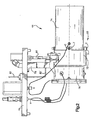
- Figure 1 is a top view, partly in section, showing an ion implanter including an ion source, beam forming and shaping structure and an implantation chamber;
- Figure 2 is an enlarged plan view of an electron shower portion of the ion implanter of Figure 1;
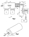
- Figure 3 is a schematic depiction of portions of an ion beam implanter showing portions of the implanter particularly suited for placement of one or more particle collectors for trapping contaminants; and
- Figure 4 is a perspective view of an ion neutralization tube that is configured as a particle trap.
-
- Turning now to the drawings, Fig. 1 depicts an ion implanter, shown generally at 10, which includes an ion source 12 for emitting ions that form an
ion beam 14 and animplantation station 16.Control electronics 11 are provided for monitoring and controlling the ion dosage received by the wafers within aprocess chamber 17 at theimplantation station 16. Theion beam 14 traverses the distance between the ion source 12 and theimplantation station 16. - The ion source 12 includes a
plasma chamber 18 defining an interior region into which source materials are injected. The source materials may include an ionizable gas or vaporized source material. Source material in solid form is deposited into a pair ofvaporizers 19. The vaporized source material is then injected into the plasma chamber. - Energy is applied to the source materials to generate positively charged ions in the
plasma chamber 18. The positively charged ions exit the plasma chamber interior through an elliptical arc slit in acover plate 20 overlying an open side of theplasma chamber 18. - An ion source utilizing microwave energy to ionize source materials is disclosed in U.S. Patent Application Serial No. 08/312,142, filed September 26, 1994, which is assigned to the assignee of the instant application.
- The
ion beam 14 travels through an evacuated path from the ion source 12 to theimplantation station 17, which is also evacuated. Evacuation of the beam path is provided byvacuum pumps 21. - Ions in the
plasma chamber 18 are extracted through the arc slit in the plasmachamber cover plate 20 and accelerated toward amass analyzing magnet 22 by a set ofelectrodes 24 adjacent the plasmachamber cover plate 20. Ions that make up theion beam 14 move from the ion source 12 into a magnetic field set up by themass analyzing magnet 22. The mass analyzing magnet is part of the ion beam forming and shaping structure 13 and is supported within amagnet housing 32. The strength of the magnetic field is controlled by thecontrol electronics 11. The magnet's field is controlled by adjusting a current through the magnet's field windings. Themass analyzing magnet 22 causes the ions traveling along theion beam 14 to move in a curved trajectory. Only those ions having an appropriate atomic mass reach theion implantation station 16. - Along the ion beam travel path from the
mass analyzing magnet 22 to theimplantation station 16, theion beam 14 is further shaped, evaluated and accelerated due to the potential drop from the high voltage of the massanalyzing magnet housing 32 to the grounded implantation chamber. - The ion beam forming and shaping structure 13 further includes a
quadrupole assembly 40, amoveable Faraday cup 42 and an ionbeam neutralization apparatus 44. Thequadruple assembly 40 includes set ofmagnets 46 oriented around theion beam 14 which are selectively energized by the control electronics (not shown) to adjust the height of theion beam 14. Thequadrupole assembly 40 is supported within ahousing 50. - Coupled to an end of the
quadruple assembly 40 facing theFaraday flag 42 is an ionbeam resolving plate 52. The resolvingplate 52 is comprised of vitreous graphite. The resolvingplate 52 includes an elongated aperture through which the ions in theion beam 14 pass as they exit thequadruple assembly 40. The resolvingplate 52 also includes four counterbored holes. Screws (not shown) fasten the resolvingplate 52 to thequadruple assembly 40. At the resolvingplate 52 the ion beam dispersion, as defined by the width of the envelope D', D", is at its minimum value, that is, the width of D', D" is at a minimum where theion beam 14 passes through the resolving plate aperture. - The resolving
plate 52 functions in conjunction with themass analyzing magnet 22 to eliminate undesirable ion species from theion beam 14. Thequadrupole assembly 40 is supported by asupport bracket 60 and asupport plate 62. Thesupport bracket 60 is coupled to an interior surface of the resolvinghousing 50 while thesupport plate 62 is coupled to an end of thehousing 50 via a plurality of screws (twoscrews 63 fastening thesupport plate 62 to thehousing 50 is seen in Fig. 1). Attached to thesupport plate 62 is a quadrupole assembly shield plate. The quadrupole assembly shield plate is comprised of vitreous graphite and includes a rectangular aperture and four counterbored holes. The counterbored holes accept screws which secure the quadruple assembly shield plate to the support plate 62 (twoscrews 70 extending through two of the counterbored holes and into thesupport plate 62 is seen in Fig. 1). The quadruple assembly shield plate protects thequadrupole assembly 40 from impact by undesirable ions having an atomic mass that is "close" to the atomic mass of the desired ion species. During operation of theimplanter 10, undesirable ions impacting an upstream facing surface of the quadruple assembly shield plate build-up the plate. - As can be seen in Fig. 1, the
Faraday flag 42 is located between thequadruple assembly 40 and the ionbeam neutralization apparatus 44. The Faraday flag is moveable relative to thehousing 50 so that it can be slid into position to intersect theion beam 14 to measure beam characteristics and, when the measurements are satisfactory, moved out of the beam line so as to not interfere with wafer implantation at theimplantation chamber 17. - The beam forming structure 13 also includes the ion
beam neutralization apparatus 44, commonly referred to as an electron shower. U.S. Patent No. 5,164,599 to Benveniste, issued November 17, 1992, discloses an electron shower apparatus in an ion beam implanter. The ions extracted from theplasma chamber 18 are positively charged. If the positive charge on the ions is not neutralized at the wafer's surface, the doped wafers will exhibit a net positive charge. As described in the '599 patent, such a net positive charge on a wafer has undesirable characteristics. - The ion
beam neutralization apparatus 44 shown in Fig. 2 includes abias aperture 70, atarget 72 and anextension tube 74. Each of thebias aperture 70, thetarget 72 and theextension tube 74 are hollow and when assembled define an open ended, cylindrical interior region through which theion beam 14 passes and is neutralized by secondary electron emissions. Theneutralizer apparatus 44 is positioned with respect to thehousing 50 by a mountingflange 76 which bolts to the resolving housing. - Extending from the mounting
flange 76 is asupport member 78 and thebias aperture 70. Thetarget 72 is secured to thesupport member 78. Theextension tube 74 is coupled to, but electrically isolated from, thetarget 72. Theextension tube 74 is grounded by a connection with a grounding terminal G. Thebias aperture 70 is energized with a negative charge V-. Thesupport member 78 defines an interior passageway (not shown) for the circulation of cooling fluid. - The
support member 78 also supports afilament feed 80 electrically coupled to a set of filaments (not shown). The filaments extend into thetarget 72 and, when energized, emit high energy electrons which are accelerated into an interior region of thetarget 72. The high energy electrons impact the interior wall of thetarget 72. The collisions of the high energy electrons with the target interior wall causes an emission of low energy electrons or so-called secondary electron emission. - A
preferred extension tube 74 of the beam neutralizer has a contaminant capturing surface and hence forms a particle trap. - Stray contaminants can become entrapped within the
ion beam 14 and carried along with the beam into thebeam neutralizer 44. Use of thetube 74 tends to collect any such contaminating particles that are within the beam and which have travel paths along the beam border. They can collide with thetube 74 and are not only removed from the beam and hence do not bombard the target within the implantation chamber, but they do not bounce off the surface of thetube 74. - The
implantation station 16 includes the evacuated implantation chamber 17 (Figures 1 and 3). Rotatably supported within theimplantation chamber 17 is a disk shaped wafer support (not shown). Wafers to be treated are positioned near a peripheral edge of the wafer support and the support is rotated by a motor (not shown) at about 1200 RPM. Theion beam 14 impinges on the wafers and treats the wafers as they rotate in a circular path. - The
implantation station 16 is pivotable with respect to thehousing 50 and is connected thereto by a flexible bellows 92. The ability to pivot theimplantation station 16 permits adjustments to the angle of incidence of theion beam 14 on the wafer implantation surface. - Figure 3 schematically indicates components of the
ion implanter 10. - The
process chamber 17 of Figure 3 is seen to include two vacuum port V3, V4 for controllably pressurizing and depressurizing theprocess chamber 17 when maintenance is performed on the implanter. Wafers are inserted into thechamber 17 by means of aload lock 110 and mounted onto a rotating support that carries the wafers through the ion beam. Photoresist on the wafers tends to be ejected off from the wafers and can collect on the interior surfaces S1, S2, S3, S4 of collector sheets mounted within the process chamber. - The particle adhering surface comprises electret fibres to attract contaminant particles.
Claims (12)
- A method of capturing and removing contaminant particles moving within an evacuated interior region of an ion implanter (10) wherein charged ions transverse an ion travel path (14) in the evacuated interior region to treat a workpiece, the steps of the method comprising:a) providing a particle collector (74) having an inward facing particle collecting surface comprising electret fibers to which contaminant particles are attracted and adhere;b) securing the particle collector (74) to the implanter (10) such that the inward facing particle collecting surface of the collector (74) defines a portion of the evacuated interior region at a location near the ion travel path (14); andc) removing the particle collector (74) from the ion beam implanter (10) at periodic time intervals to remove particles adhering to the collector (74) from the evacuated interior region of the implanter (10).
- The method of capturing and removing contaminant particles as set forth in claim 1 wherein the electret fibers attract and secure contaminant particles to the particle collector (74) by electrostatic attraction.
- The method of capturing and removing contaminant particles as set forth in claim 1 wherein the step of securing the particle collector (74) to the implanter (10) is performed by coating an attachment surface (S5, S6) with a partially cured elastomer which secures the collector to an inner wall of the implanter such that the inward facing particle collecting surface of the collector (74) is positioned within the evacuated interior region at a location near the ion travel path.
- The method of capturing and removing contaminant particles as set forth in claim 3 wherein the coating of partially cured elastomers includes the step of partially curing a silicone elastomer.
- The method of capturing and removing contaminant particles as set forth in claim 3 wherein the particle collecting surface of the particle collector (74) is positioned inside a process chamber (17) of the implanter (10) that contains one or more workpieces.
- The method of capturing and removing contaminant particles as set forth in claim 5 wherein the particle collector (74) is attached to an interior surface of the process chamber (17) facing a treatment surface of the workpiece.
- The method of capturing and removing contaminant particles as set forth in claim 3 wherein the particle collector particle collecting surface is within a clear field of view of a resolving housing (112) of the implanter.
- The method of capturing and removing contaminant particles as set forth in claim 7 wherein the particle collector (74) is attached to an interior surface (S5, S6) of the resolving housing (112).
- In combination, an ion implanter (10) and apparatus for trapping and removing contaminant particles moving in an evacuated region of the implanter traversed by ions moving toward a workpiece comprising:a) a collector (74) having an inward facing particle collecting surface to which contaminant particles readily adhere which defines a portion of the evacuated interior region of the implanter (10) and wherein the implanter comprises a source (12) for emitting ions and beam forming structure (24, 22, 20) for creating an ion beam for treatment of one or more workpieces;b) a support comprising means for supporting the inward facing particle collecting surface characterised in that the inward facing particle collecting surface comprises electret fibers for attracting contaminant particles.
- The ion implanter and apparatus as set forth in claim 9 wherein the electret fibers attract and secure contaminant particles to the particle collecting surface by electrostatic attraction.
- The method of capturing and removing contaminant particles as set forth in claim 1 wherein the particle collector (74) has an annular shape and wherein the particle collector collecting surface surrounds the ion beam path (14).
- The method of capturing and removing contaminant particles as set forth in claim 11 wherein the particle collecting surface surrounds the ion beam on its way to the workpiece such that the contaminants are intercepted before reaching the workpiece.
Applications Claiming Priority (2)
| Application Number | Priority Date | Filing Date | Title |
|---|---|---|---|
| US08/574,242 US5656092A (en) | 1995-12-18 | 1995-12-18 | Apparatus for capturing and removing contaminant particles from an interior region of an ion implanter |
| US574242 | 1995-12-18 |
Publications (3)
| Publication Number | Publication Date |
|---|---|
| EP0780877A2 EP0780877A2 (en) | 1997-06-25 |
| EP0780877A3 EP0780877A3 (en) | 1999-02-10 |
| EP0780877B1 true EP0780877B1 (en) | 2003-02-19 |
Family
ID=24295284
Family Applications (1)
| Application Number | Title | Priority Date | Filing Date |
|---|---|---|---|
| EP96308758A Expired - Lifetime EP0780877B1 (en) | 1995-12-18 | 1996-12-04 | Method and apparatus for capturing and removing contaminant particles from an interior region of an ion implanter |
Country Status (8)
| Country | Link |
|---|---|
| US (2) | US5656092A (en) |
| EP (1) | EP0780877B1 (en) |
| JP (1) | JP4013086B2 (en) |
| KR (1) | KR100292085B1 (en) |
| CN (1) | CN1158494A (en) |
| CA (1) | CA2191115C (en) |
| DE (1) | DE69626265T2 (en) |
| TW (1) | TW386309B (en) |
Cited By (1)
| Publication number | Priority date | Publication date | Assignee | Title |
|---|---|---|---|---|
| EP1014420B1 (en) * | 1998-12-21 | 2006-05-17 | Axcelis Technologies, Inc. | Lateral stress relief mechanism for vacuum bellows |
Families Citing this family (32)
| Publication number | Priority date | Publication date | Assignee | Title |
|---|---|---|---|---|
| US5903009A (en) * | 1997-09-08 | 1999-05-11 | Eaton Corporation | Biased and serrated extension tube for ion implanter electron shower |
| US5909031A (en) * | 1997-09-08 | 1999-06-01 | Eaton Corporation | Ion implanter electron shower having enhanced secondary electron emission |
| US6231054B1 (en) * | 1998-12-21 | 2001-05-15 | Axcelis Technologies, Inc. | Elastomeric sliding seal for vacuum bellows |
| US6259105B1 (en) * | 1999-05-10 | 2001-07-10 | Axcelis Technologies, Inc. | System and method for cleaning silicon-coated surfaces in an ion implanter |
| US6476399B1 (en) | 2000-09-01 | 2002-11-05 | Axcelis Technologies, Inc. | System and method for removing contaminant particles relative to an ion beam |
| US6534775B1 (en) | 2000-09-01 | 2003-03-18 | Axcelis Technologies, Inc. | Electrostatic trap for particles entrained in an ion beam |
| US6525326B1 (en) | 2000-09-01 | 2003-02-25 | Axcelis Technologies, Inc. | System and method for removing particles entrained in an ion beam |
| JP2002105628A (en) * | 2000-10-03 | 2002-04-10 | Nissin Electric Co Ltd | Vacuum arc vapor deposition apparatus |
| KR100385917B1 (en) * | 2001-06-27 | 2003-06-02 | 삼성전자주식회사 | Vacuum pumping apparatus of ion implanting system |
| US20050133736A1 (en) * | 2003-12-17 | 2005-06-23 | Otto Chen | Ion implantation apparatus and partical collection structure thereof |
| US7078710B2 (en) * | 2004-06-15 | 2006-07-18 | International Business Machines Corporation | Ion beam system |
| TWI256697B (en) * | 2004-07-08 | 2006-06-11 | Advanced Ion Beam Technology I | Method for preventing wafer defect for a batch-type ion implanter spinning direction particle |
| US7205556B2 (en) * | 2004-10-01 | 2007-04-17 | Axcelis Technologies, Inc. | Bellows liner for an ion beam implanter |
| KR100848959B1 (en) * | 2004-11-19 | 2008-07-29 | 가부시키가이샤 아루박 | Ion implantation device |
| US7173260B2 (en) * | 2004-12-22 | 2007-02-06 | Axcelis Technologies, Inc. | Removing byproducts of physical and chemical reactions in an ion implanter |
| CN101233597B (en) * | 2005-06-03 | 2011-04-20 | 艾克塞利斯技术公司 | Charged Beam Collection and Particle Attractors |
| US7199383B2 (en) * | 2005-08-25 | 2007-04-03 | United Microelectronics Corp. | Method for reducing particles during ion implantation |
| KR100677046B1 (en) * | 2005-09-21 | 2007-02-01 | 동부일렉트로닉스 주식회사 | Ion implantation device |
| US7358508B2 (en) * | 2005-11-10 | 2008-04-15 | Axcelis Technologies, Inc. | Ion implanter with contaminant collecting surface |
| KR100800946B1 (en) * | 2006-08-21 | 2008-02-04 | 동부일렉트로닉스 주식회사 | Particle removal structure of ion implanter |
| JP4660452B2 (en) * | 2006-09-30 | 2011-03-30 | 株式会社フェローテック | Expanded tube plasma generator |
| US20080157007A1 (en) * | 2006-12-27 | 2008-07-03 | Varian Semiconductor Equipment Associates, Inc. | Active particle trapping for process control |
| US20080164427A1 (en) * | 2007-01-09 | 2008-07-10 | Applied Materials, Inc. | Ion implanters |
| JP5189784B2 (en) * | 2007-03-30 | 2013-04-24 | 株式会社フェローテック | Plasma generator with electrical neutralization around the plasma gun |
| US8000080B2 (en) | 2007-12-07 | 2011-08-16 | Varian Semiconductor Equipment Associates, Inc. | Particle trap |
| US20090179158A1 (en) * | 2008-01-16 | 2009-07-16 | Varian Semiconductor Equpiment Associate, Inc. | In-vacuum protective liners |
| JP5644085B2 (en) * | 2009-06-10 | 2014-12-24 | 富士通株式会社 | Film forming apparatus and film forming method |
| JP5606777B2 (en) * | 2010-04-22 | 2014-10-15 | 株式会社フェローテック | Plasma flow generation method, plasma processing method, plasma generator, and plasma processing apparatus |
| US8963107B2 (en) * | 2012-01-12 | 2015-02-24 | Axcelis Technologies, Inc. | Beam line design to reduce energy contamination |
| CN105097460A (en) * | 2014-05-09 | 2015-11-25 | 中芯国际集成电路制造(上海)有限公司 | Method for solving problem of path pollution of ion implanter |
| US11222768B2 (en) * | 2018-09-07 | 2022-01-11 | Varian Semiconductor Equipment Associates, Inc. | Foam in ion implantation system |
| CN111261482B (en) * | 2018-11-30 | 2023-02-28 | 夏泰鑫半导体(青岛)有限公司 | Ion implantation device and method for trapping pollutant particles during ion implantation |
Family Cites Families (7)
| Publication number | Priority date | Publication date | Assignee | Title |
|---|---|---|---|---|
| US4022928A (en) * | 1975-05-22 | 1977-05-10 | Piwcyzk Bernhard P | Vacuum deposition methods and masking structure |
| EP0140975A4 (en) * | 1983-03-18 | 1988-01-07 | Matsushita Electric Industrial Co Ltd | REACTIVE ION ETCHING APPARATUS. |
| DE3588237T2 (en) * | 1984-09-19 | 2002-11-14 | Applied Materials, Inc. | Device for scanning wafers by an ion beam |
| US5135634A (en) * | 1991-02-14 | 1992-08-04 | Sputtered Films, Inc. | Apparatus for depositing a thin layer of sputtered atoms on a member |
| EP0648861A1 (en) * | 1993-10-15 | 1995-04-19 | Applied Materials, Inc. | Semiconductor processing apparatus |
| EP0648858A1 (en) * | 1993-10-15 | 1995-04-19 | Applied Materials, Inc. | Methods of coating plasma etch chambers and apparatus for plasma etching workpieces |
| US5455426A (en) * | 1994-06-15 | 1995-10-03 | Texas Instruments Incorporated | Target chamber shielding |
-
1995
- 1995-12-18 US US08/574,242 patent/US5656092A/en not_active Expired - Fee Related
-
1996
- 1996-11-22 CA CA002191115A patent/CA2191115C/en not_active Expired - Fee Related
- 1996-12-04 DE DE69626265T patent/DE69626265T2/en not_active Expired - Fee Related
- 1996-12-04 EP EP96308758A patent/EP0780877B1/en not_active Expired - Lifetime
- 1996-12-05 TW TW085114993A patent/TW386309B/en not_active IP Right Cessation
- 1996-12-09 US US08/762,320 patent/US5670217A/en not_active Expired - Fee Related
- 1996-12-17 KR KR1019960066795A patent/KR100292085B1/en not_active Expired - Fee Related
- 1996-12-18 JP JP33804496A patent/JP4013086B2/en not_active Expired - Lifetime
- 1996-12-18 CN CN96116703A patent/CN1158494A/en active Pending
Cited By (1)
| Publication number | Priority date | Publication date | Assignee | Title |
|---|---|---|---|---|
| EP1014420B1 (en) * | 1998-12-21 | 2006-05-17 | Axcelis Technologies, Inc. | Lateral stress relief mechanism for vacuum bellows |
Also Published As
| Publication number | Publication date |
|---|---|
| US5656092A (en) | 1997-08-12 |
| CN1158494A (en) | 1997-09-03 |
| US5670217A (en) | 1997-09-23 |
| JPH09190794A (en) | 1997-07-22 |
| TW386309B (en) | 2000-04-01 |
| EP0780877A2 (en) | 1997-06-25 |
| EP0780877A3 (en) | 1999-02-10 |
| CA2191115A1 (en) | 1997-06-19 |
| JP4013086B2 (en) | 2007-11-28 |
| KR970052173A (en) | 1997-07-29 |
| KR100292085B1 (en) | 2001-06-01 |
| CA2191115C (en) | 2002-02-05 |
| DE69626265T2 (en) | 2003-12-04 |
| DE69626265D1 (en) | 2003-03-27 |
Similar Documents
| Publication | Publication Date | Title |
|---|---|---|
| US5670217A (en) | Method for capturing and removing contaminant particles from an interior region of an ion implanter | |
| EP0757373B1 (en) | In situ removal of contaminants from the interior surfaces of an ion beam implanter | |
| CA2181076C (en) | Method and apparatus for in situ removal of contaminants from ion beam neutralization and implantation apparatuses | |
| KR101236563B1 (en) | Charged beam dump and particle attractor | |
| EP1314181B1 (en) | Electrostatic trap for particles entrained in an ion beam | |
| CN105474349B (en) | Voltage Modulation of Extraction Electrode Assembly in Ion Implantation System | |
| WO2011126538A2 (en) | In-vacuum beam defining aperture cleaning for particle reduction | |
| US6476399B1 (en) | System and method for removing contaminant particles relative to an ion beam | |
| EP1314182B1 (en) | System and method for removing particles entrained in an ion beam | |
| US20050133736A1 (en) | Ion implantation apparatus and partical collection structure thereof | |
| US8242469B2 (en) | Adjustable louvered plasma electron flood enclosure | |
| NL1005011C2 (en) | Absorbing and removing contaminant particles inside ion implant device, using removable collector with particle adhesion surface |
Legal Events
| Date | Code | Title | Description |
|---|---|---|---|
| PUAI | Public reference made under article 153(3) epc to a published international application that has entered the european phase |
Free format text: ORIGINAL CODE: 0009012 |
|
| AK | Designated contracting states |
Kind code of ref document: A2 Designated state(s): DE ES FR GB IT SE |
|
| PUAL | Search report despatched |
Free format text: ORIGINAL CODE: 0009013 |
|
| AK | Designated contracting states |
Kind code of ref document: A3 Designated state(s): DE ES FR GB IT SE |
|
| 17P | Request for examination filed |
Effective date: 19990702 |
|
| 17Q | First examination report despatched |
Effective date: 20000511 |
|
| RAP1 | Party data changed (applicant data changed or rights of an application transferred) |
Owner name: AXCELIS TECHNOLOGIES, INC. |
|
| GRAG | Despatch of communication of intention to grant |
Free format text: ORIGINAL CODE: EPIDOS AGRA |
|
| GRAG | Despatch of communication of intention to grant |
Free format text: ORIGINAL CODE: EPIDOS AGRA |
|
| GRAG | Despatch of communication of intention to grant |
Free format text: ORIGINAL CODE: EPIDOS AGRA |
|
| GRAH | Despatch of communication of intention to grant a patent |
Free format text: ORIGINAL CODE: EPIDOS IGRA |
|
| GRAH | Despatch of communication of intention to grant a patent |
Free format text: ORIGINAL CODE: EPIDOS IGRA |
|
| GRAA | (expected) grant |
Free format text: ORIGINAL CODE: 0009210 |
|
| AK | Designated contracting states |
Designated state(s): DE ES FR GB IT SE |
|
| REG | Reference to a national code |
Ref country code: GB Ref legal event code: FG4D |
|
| REF | Corresponds to: |
Ref document number: 69626265 Country of ref document: DE Date of ref document: 20030327 Kind code of ref document: P |
|
| PG25 | Lapsed in a contracting state [announced via postgrant information from national office to epo] |
Ref country code: SE Free format text: LAPSE BECAUSE OF FAILURE TO SUBMIT A TRANSLATION OF THE DESCRIPTION OR TO PAY THE FEE WITHIN THE PRESCRIBED TIME-LIMIT Effective date: 20030519 |
|
| ET | Fr: translation filed | ||
| PG25 | Lapsed in a contracting state [announced via postgrant information from national office to epo] |
Ref country code: ES Free format text: LAPSE BECAUSE OF FAILURE TO SUBMIT A TRANSLATION OF THE DESCRIPTION OR TO PAY THE FEE WITHIN THE PRESCRIBED TIME-LIMIT Effective date: 20030828 |
|
| PLBE | No opposition filed within time limit |
Free format text: ORIGINAL CODE: 0009261 |
|
| STAA | Information on the status of an ep patent application or granted ep patent |
Free format text: STATUS: NO OPPOSITION FILED WITHIN TIME LIMIT |
|
| 26N | No opposition filed |
Effective date: 20031120 |
|
| PGFP | Annual fee paid to national office [announced via postgrant information from national office to epo] |
Ref country code: DE Payment date: 20071228 Year of fee payment: 12 |
|
| PGFP | Annual fee paid to national office [announced via postgrant information from national office to epo] |
Ref country code: IT Payment date: 20081213 Year of fee payment: 13 |
|
| PGFP | Annual fee paid to national office [announced via postgrant information from national office to epo] |
Ref country code: FR Payment date: 20081205 Year of fee payment: 13 |
|
| PGFP | Annual fee paid to national office [announced via postgrant information from national office to epo] |
Ref country code: GB Payment date: 20081110 Year of fee payment: 13 |
|
| PG25 | Lapsed in a contracting state [announced via postgrant information from national office to epo] |
Ref country code: DE Free format text: LAPSE BECAUSE OF NON-PAYMENT OF DUE FEES Effective date: 20090701 |
|
| GBPC | Gb: european patent ceased through non-payment of renewal fee |
Effective date: 20091204 |
|
| REG | Reference to a national code |
Ref country code: FR Ref legal event code: ST Effective date: 20100831 |
|
| PG25 | Lapsed in a contracting state [announced via postgrant information from national office to epo] |
Ref country code: FR Free format text: LAPSE BECAUSE OF NON-PAYMENT OF DUE FEES Effective date: 20091231 |
|
| PG25 | Lapsed in a contracting state [announced via postgrant information from national office to epo] |
Ref country code: GB Free format text: LAPSE BECAUSE OF NON-PAYMENT OF DUE FEES Effective date: 20091204 |
|
| PG25 | Lapsed in a contracting state [announced via postgrant information from national office to epo] |
Ref country code: IT Free format text: LAPSE BECAUSE OF NON-PAYMENT OF DUE FEES Effective date: 20091204 |