EP0779521A1 - X-ray detector for automatic exposure control of an imaging apparatus - Google Patents
X-ray detector for automatic exposure control of an imaging apparatus Download PDFInfo
- Publication number
- EP0779521A1 EP0779521A1 EP96308922A EP96308922A EP0779521A1 EP 0779521 A1 EP0779521 A1 EP 0779521A1 EP 96308922 A EP96308922 A EP 96308922A EP 96308922 A EP96308922 A EP 96308922A EP 0779521 A1 EP0779521 A1 EP 0779521A1
- Authority
- EP
- European Patent Office
- Prior art keywords
- layer
- ray detector
- electrode
- semiconductive material
- ray
- Prior art date
- Legal status (The legal status is an assumption and is not a legal conclusion. Google has not performed a legal analysis and makes no representation as to the accuracy of the status listed.)
- Withdrawn
Links
- 238000003384 imaging method Methods 0.000 title description 8
- 239000000463 material Substances 0.000 claims abstract description 26
- 239000000758 substrate Substances 0.000 claims abstract description 12
- 239000004065 semiconductor Substances 0.000 claims abstract description 7
- 239000004020 conductor Substances 0.000 claims abstract description 6
- 230000004044 response Effects 0.000 claims abstract description 6
- OKTJSMMVPCPJKN-UHFFFAOYSA-N Carbon Chemical compound [C] OKTJSMMVPCPJKN-UHFFFAOYSA-N 0.000 claims abstract description 5
- 229910004613 CdTe Inorganic materials 0.000 claims abstract description 5
- 229910004611 CdZnTe Inorganic materials 0.000 claims abstract description 5
- 229910021417 amorphous silicon Inorganic materials 0.000 claims abstract description 5
- 229910052799 carbon Inorganic materials 0.000 claims abstract description 5
- 239000002131 composite material Substances 0.000 claims abstract description 5
- 239000011159 matrix material Substances 0.000 claims description 5
- 238000002059 diagnostic imaging Methods 0.000 claims 1
- 150000002500 ions Chemical class 0.000 description 3
- 239000007787 solid Substances 0.000 description 3
- 230000005540 biological transmission Effects 0.000 description 2
- 230000000712 assembly Effects 0.000 description 1
- 238000000429 assembly Methods 0.000 description 1
- 230000002238 attenuated effect Effects 0.000 description 1
- 150000001721 carbon Chemical class 0.000 description 1
- 238000007796 conventional method Methods 0.000 description 1
- 238000010586 diagram Methods 0.000 description 1
- 230000002708 enhancing effect Effects 0.000 description 1
- 239000000835 fiber Substances 0.000 description 1
- 238000002594 fluoroscopy Methods 0.000 description 1
- AMGQUBHHOARCQH-UHFFFAOYSA-N indium;oxotin Chemical compound [In].[Sn]=O AMGQUBHHOARCQH-UHFFFAOYSA-N 0.000 description 1
- 230000001939 inductive effect Effects 0.000 description 1
- 230000007774 longterm Effects 0.000 description 1
- 238000004519 manufacturing process Methods 0.000 description 1
- 238000001465 metallisation Methods 0.000 description 1
- 230000026954 response to X-ray Effects 0.000 description 1
- 238000001429 visible spectrum Methods 0.000 description 1
Images

Classifications
-
- G—PHYSICS
- G01—MEASURING; TESTING
- G01T—MEASUREMENT OF NUCLEAR OR X-RADIATION
- G01T1/00—Measuring X-radiation, gamma radiation, corpuscular radiation, or cosmic radiation
- G01T1/16—Measuring radiation intensity
- G01T1/24—Measuring radiation intensity with semiconductor detectors
-
- G—PHYSICS
- G01—MEASURING; TESTING
- G01T—MEASUREMENT OF NUCLEAR OR X-RADIATION
- G01T1/00—Measuring X-radiation, gamma radiation, corpuscular radiation, or cosmic radiation
- G01T1/16—Measuring radiation intensity
- G01T1/26—Measuring radiation intensity with resistance detectors
-
- H—ELECTRICITY
- H04—ELECTRIC COMMUNICATION TECHNIQUE
- H04N—PICTORIAL COMMUNICATION, e.g. TELEVISION
- H04N23/00—Cameras or camera modules comprising electronic image sensors; Control thereof
- H04N23/30—Cameras or camera modules comprising electronic image sensors; Control thereof for generating image signals from X-rays
-
- H—ELECTRICITY
- H05—ELECTRIC TECHNIQUES NOT OTHERWISE PROVIDED FOR
- H05G—X-RAY TECHNIQUE
- H05G1/00—X-ray apparatus involving X-ray tubes; Circuits therefor
- H05G1/08—Electrical details
- H05G1/26—Measuring, controlling or protecting
- H05G1/30—Controlling
- H05G1/38—Exposure time
- H05G1/42—Exposure time using arrangements for switching when a predetermined dose of radiation has been applied, e.g. in which the switching instant is determined by measuring the electrical energy supplied to the tube
- H05G1/44—Exposure time using arrangements for switching when a predetermined dose of radiation has been applied, e.g. in which the switching instant is determined by measuring the electrical energy supplied to the tube in which the switching instant is determined by measuring the amount of radiation directly
-
- H—ELECTRICITY
- H10—SEMICONDUCTOR DEVICES; ELECTRIC SOLID-STATE DEVICES NOT OTHERWISE PROVIDED FOR
- H10F—INORGANIC SEMICONDUCTOR DEVICES SENSITIVE TO INFRARED RADIATION, LIGHT, ELECTROMAGNETIC RADIATION OF SHORTER WAVELENGTH OR CORPUSCULAR RADIATION
- H10F39/00—Integrated devices, or assemblies of multiple devices, comprising at least one element covered by group H10F30/00, e.g. radiation detectors comprising photodiode arrays
- H10F39/10—Integrated devices
- H10F39/12—Image sensors
Definitions
- the present invention relates to automatic exposure control systems for x-ray imaging apparatus; and more particularly to x-ray detectors utilized in such exposure control systems.
- Conventional fluoroscopic x-ray imaging equipment include a source for projecting a beam of x-rays through an object being imaged, such as a medical patient.
- the portion of the beam which passes through the patient impinges upon an x-ray detector which converts the x-rays attenuated by the patient into photons which then are converted into an electric image signal.
- the x-ray detector may comprise an image intensifier tube and a video camera, or a combination of a scintillator in front of a two-dimensional photodetector array.
- the electrical image signal from either type of detector is processed to display an image of the patient on a video monitor.
- the image signal also is applied to the input of a feedback loop which responds to the level of the image signal by producing a control signal which regulates the x-ray exposure and thus brightness of the image on the video monitor.
- a feedback loop which responds to the level of the image signal by producing a control signal which regulates the x-ray exposure and thus brightness of the image on the video monitor.
- the control signal regulates the biasing of the x-ray tube and the gain of the video camera.
- This feedback control loop ensures that the image produced in the video monitor has sufficient brightness and contrast for proper viewing by an x-ray technician or physician.
- a general object of the present invention is to provide a separate x-ray detector for the automatic exposure control which is not part of the image detector utilized to produce the image displayed on the video monitor.
- Another object of the present invention is to provide an x-ray detector which can be placed in front of or behind the image detector with respect to the source of x-rays.
- a further object of the present invention is to provide such a detector which has minimal x-ray attenuation variations so as to minimize inducing visible image artifacts.
- an x-ray detector for an automatic exposure control system that comprises a substrate having a major surface on which a first electrode layer is formed.
- a layer of semiconductive material is deposited on the first electrode and has an electrical characteristic which varies in response to impingement of x-rays.
- this latter layer comprises homogeneous semiconductive material, such as CdTe, CdZnTe or amorphous silicon.
- a second electrode layer is formed on the layer of semiconductor material remote from the first electrode layer.
- One of the first and second electrode layers is divided into a plurality of conductive elements thereby defining a plurality of regions in the layer of semiconductive material adjacent to each of the plurality of conductive elements.
- the semiconductive layer acts as a solid state ion chamber and can be operated in a photovoltaic mode in which an electrical current is produced in this layer in response to x-ray bombardment or operated in a photoconductivity mode in which the conductivity of the semiconductive layer is altered by the x-rays. In either mode, the intensity of x-rays striking the various regions can be measured by sensing the electric current flow between each of the conductive elements and the other electrode layer.
- an x-ray imaging system 14 includes an x-ray tube 15 which emits an x-ray beam 17 when excited by power supply 16. As illustrated, the x-ray beam 17 is directed through a patient 18 lying on an x-ray transmissive table 20 and impinges upon a detector assembly designated 22.
- the detector assembly 22 comprises an automatic exposure control (AEC) detector 23 and an imaging device 25 formed in this embodiment by a scintillator 24 in front of a two-dimensional photodetector array 26.
- the scintillator 24 converts the x-ray protons to lower energy photons in the visible spectrum and the photodetector array 26, contiguous with the scintillator, converts the light photons into electrical signals.
- the scintillator 24 and photodetector array 26 are well-known components of conventional x-ray detector assemblies used in previous x-ray imaging systems.
- the AEC detector 23 can be located on the remote side of the detector assembly 22 from the x-ray tube 15.
- the AEC detector 23 may be used with other types of imaging devices 25, such as an image intensifier with a video camera, or even x-ray film.
- a detector controller 27 contains electronics for operating the photodetector array 26 to acquire an image by reading a signal from each photodetector element in the two-dimensional array.
- the output signal from the photodetector array 26 is coupled to an image processor 28 that includes circuitry for processing and enhancing the x-ray image signal.
- the processed image then is displayed on a video monitor 32 and may be archived in an image storage device 30.
- the overall operation of the x-ray imaging system 14 is governed by a system controller 36 which receives commands from the operator via an operator panel 38.
- the x-ray exposure is controlled automatically by a feedback loop that includes the AEC x-ray detector 23 and an exposure control circuit 34.
- the AEC x-ray detector 23 produces a plurality of electrical signals corresponding to the intensity of the x-rays impinging different regions of the detector. Those signals are applied to inputs of the exposure control circuit 34 along with signals from the system controller 36 designating the desired x-ray dose selected by the operator.
- the exposure control circuit 34 responds to these input signals by producing a command signal for the x-ray tube power supply 16 which defines the bias voltage and filament current levels for the x-ray tube 15 to produce the desired x-ray dosage.
- the exposure control 34 responds to the AEC detector signal, which indicates the intensity of the x-rays passing through the patient 18, by commanding the power supply 16 to increase or decrease the bias voltage and filament current for the x-ray tube 15 to achieve an optimal x-ray exposure for a satisfactory image.
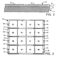
- the present invention relates to the unique multiple layer structure of the AEC detector 23 shown in Figure 2.
- the active layers are formed on a surface of substrate 40 which preferably comprises a low density carbon composite material containing fibers in a matrix material.
- substrate 40 which preferably comprises a low density carbon composite material containing fibers in a matrix material.
- Use of such conventional carbon composites is particularly desirable when the AEC detector 23 is placed in front of the photodetector array 26, as the low density material is x-ray transmissive and provides uniform x-ray attenuation.
- the carbon composite does not induce artifacts in the signal produced by photodetector array 26 enabling the AEC x-ray detector 23 to be placed in front of the scintillator 24 and photodetector array 26.
- the x-ray transmission characteristics of the substrate 40 are not critical and other materials may be employed.
- a uniform first electrode layer 42 is applied over the entire major surface on one side of substrate 40 and serves as a high voltage bias electrode.
- the first electrode layer 42 is formed by either metallization or other conductive material, such as indium tin oxide, deposited by conventional techniques.
- the first electrode layer 42 is relatively thin so as to minimally attenuate x-rays passing therethrough.
- a thin semiconductive layer 44 such as molecular beam epitaxially deposited CdTe, CdZnTe, amorphous silicon or other semiconductor material, extends over the first electrode layer 42.
- the semiconductive layer 44 has a good response to x-rays, high efficiency in converting x-rays to an electrical signal, uniform x-ray transmission and long term x-ray stability.
- the layer 44 of semiconductive material preferably is homogeneous, i.e. p-n junctions are not formed.
- the semiconductive material acts as a solid state ionization chamber in which charged ions are formed in proportion to the intensity of the x-rays which strike the layer. By collecting the ions to form an electrical signal the x-ray intensity can be measured.
- a second electrode layer 46 comprising a plurality of conductive elements 47 and 48 in a pattern which enables the sensing of x-rays impinging different regions of the semiconductive layer.
- the second electrode layer 46 is relatively thin so as to minimally attenuate x-rays passing therethrough.
- An exemplary pattern of conductive elements 51-66 is shown in Figure 3. This pattern is a four-by-four matrix of rectangular elements on the surface of semiconductive layer 44.
- Four conductive elements 51, 55, 59, and 63 along one edge 71 of the AEC detector 23 are connected electrically to individual contact pads 68 in a first margin 70 along that edge 71.
- An additional set of four contact pads 72 is formed on the first margin 70 with conductive stripes extending therefrom between the outer electrode elements to interior electrode elements 52, 56, 60 and 64.
- the opposite side 73 of the AEC detector 23 has a second margin 74 with for contact pads 76 connected to outer electrode elements 54, 58, 62 and 66 immediately adjacent the second margin.
- Another set of four contact pads 78 is formed within the second margin 74 with separate conductors extending therefrom between the outer electrode elements to four interior electrode elements 53, 57, 61, and 65.
- the second margin 74 has an additional contact pad 80 which extends through an opening in the semiconductive layer 44 to provide electrical contact with the first electrode layer 42.
- the plurality of contact pads 68, 72, 76, 78 and 80 are connected by individual wires to separate inputs of the exposure control 34.
- Electrodes of the second electrode layer 46 are within the purview of the present invention.
- the electrode elements do not have to be spaced over the entire surface of the substrate, but may be positioned periodically on the surface or only at the corners depending upon the degree of x-ray sensing desired for the automatic exposure control.
- the semiconductive layer 44 can be configured to operate in any common solid state mode, such as the photovoltaic mode or the photoconductivity mode.
- the exposure control 34 selectively senses the electrical signal produced in the semiconductor material between the first electrode layer 42 and each of the electrode elements 51-66 of the second electrode layer 46. In doing so, the exposure control 34 may apply a high voltage to the first electrode layer 42 to bias the semiconductive layer 44 for drift and collection of x-ray induced charges therein. The collection of charge produces an electrical signal between the first and second electrode layers 42 and 46 which can be locally sensed by detecting the signal at each of the electrode elements 51-66 of the second layer 46.
- the exposure control is able to detect the intensity of x-rays striking different portions of the AEC detector 23 and determine from those various signal samples, the power supply command to produce the desired x-ray dosage for optimal image production.
Landscapes
- Health & Medical Sciences (AREA)
- Life Sciences & Earth Sciences (AREA)
- Spectroscopy & Molecular Physics (AREA)
- Molecular Biology (AREA)
- High Energy & Nuclear Physics (AREA)
- General Physics & Mathematics (AREA)
- Physics & Mathematics (AREA)
- General Health & Medical Sciences (AREA)
- Toxicology (AREA)
- Engineering & Computer Science (AREA)
- Signal Processing (AREA)
- Multimedia (AREA)
- Measurement Of Radiation (AREA)
- Apparatus For Radiation Diagnosis (AREA)
- Solid State Image Pick-Up Elements (AREA)
- Transforming Light Signals Into Electric Signals (AREA)
- Light Receiving Elements (AREA)
Abstract
Description
- The present invention relates to automatic exposure control systems for x-ray imaging apparatus; and more particularly to x-ray detectors utilized in such exposure control systems.
- Conventional fluoroscopic x-ray imaging equipment include a source for projecting a beam of x-rays through an object being imaged, such as a medical patient. The portion of the beam which passes through the patient impinges upon an x-ray detector which converts the x-rays attenuated by the patient into photons which then are converted into an electric image signal. The x-ray detector may comprise an image intensifier tube and a video camera, or a combination of a scintillator in front of a two-dimensional photodetector array. The electrical image signal from either type of detector is processed to display an image of the patient on a video monitor.
- The image signal also is applied to the input of a feedback loop which responds to the level of the image signal by producing a control signal which regulates the x-ray exposure and thus brightness of the image on the video monitor. An example of this type of feedback control is described in U.S. Patent No. 4,573,183. The control signal regulates the biasing of the x-ray tube and the gain of the video camera. This feedback control loop ensures that the image produced in the video monitor has sufficient brightness and contrast for proper viewing by an x-ray technician or physician.
- A general object of the present invention is to provide a separate x-ray detector for the automatic exposure control which is not part of the image detector utilized to produce the image displayed on the video monitor.
- Another object of the present invention is to provide an x-ray detector which can be placed in front of or behind the image detector with respect to the source of x-rays.
- A further object of the present invention is to provide such a detector which has minimal x-ray attenuation variations so as to minimize inducing visible image artifacts.
- These and other objects are fulfilled by an x-ray detector for an automatic exposure control system that comprises a substrate having a major surface on which a first electrode layer is formed. A layer of semiconductive material is deposited on the first electrode and has an electrical characteristic which varies in response to impingement of x-rays. In the preferred embodiment, this latter layer comprises homogeneous semiconductive material, such as CdTe, CdZnTe or amorphous silicon. A second electrode layer is formed on the layer of semiconductor material remote from the first electrode layer. One of the first and second electrode layers is divided into a plurality of conductive elements thereby defining a plurality of regions in the layer of semiconductive material adjacent to each of the plurality of conductive elements.
- The semiconductive layer acts as a solid state ion chamber and can be operated in a photovoltaic mode in which an electrical current is produced in this layer in response to x-ray bombardment or operated in a photoconductivity mode in which the conductivity of the semiconductive layer is altered by the x-rays. In either mode, the intensity of x-rays striking the various regions can be measured by sensing the electric current flow between each of the conductive elements and the other electrode layer.
- An embodiment of the invention will now be described, by way of example, with reference to the accompanying drawings, in which:-
- FIGURE 1 is a block diagram of an x-ray fluoroscopy system utilizing the present invention;
- FIGURE 2 is a cross-section view through the x-ray detector for automatic exposure controller shown in Figure 1; and
- FIGURE 3 is a top view of the x-ray detector for the automatic exposure controller.
- With initial reference to Figure 1, an
x-ray imaging system 14 includes anx-ray tube 15 which emits anx-ray beam 17 when excited bypower supply 16. As illustrated, thex-ray beam 17 is directed through apatient 18 lying on an x-ray transmissive table 20 and impinges upon a detector assembly designated 22. Thedetector assembly 22 comprises an automatic exposure control (AEC)detector 23 and animaging device 25 formed in this embodiment by ascintillator 24 in front of a two-dimensional photodetector array 26. Thescintillator 24 converts the x-ray protons to lower energy photons in the visible spectrum and thephotodetector array 26, contiguous with the scintillator, converts the light photons into electrical signals. Thescintillator 24 andphotodetector array 26 are well-known components of conventional x-ray detector assemblies used in previous x-ray imaging systems. Alternatively, theAEC detector 23 can be located on the remote side of thedetector assembly 22 from thex-ray tube 15. TheAEC detector 23 may be used with other types ofimaging devices 25, such as an image intensifier with a video camera, or even x-ray film. - A
detector controller 27 contains electronics for operating thephotodetector array 26 to acquire an image by reading a signal from each photodetector element in the two-dimensional array. The output signal from thephotodetector array 26 is coupled to animage processor 28 that includes circuitry for processing and enhancing the x-ray image signal. The processed image then is displayed on avideo monitor 32 and may be archived in animage storage device 30. - The overall operation of the
x-ray imaging system 14 is governed by asystem controller 36 which receives commands from the operator via anoperator panel 38. - The x-ray exposure is controlled automatically by a feedback loop that includes the
AEC x-ray detector 23 and anexposure control circuit 34. TheAEC x-ray detector 23 produces a plurality of electrical signals corresponding to the intensity of the x-rays impinging different regions of the detector. Those signals are applied to inputs of theexposure control circuit 34 along with signals from thesystem controller 36 designating the desired x-ray dose selected by the operator. Theexposure control circuit 34 responds to these input signals by producing a command signal for the x-raytube power supply 16 which defines the bias voltage and filament current levels for thex-ray tube 15 to produce the desired x-ray dosage. During the x-ray exposure, theexposure control 34 responds to the AEC detector signal, which indicates the intensity of the x-rays passing through thepatient 18, by commanding thepower supply 16 to increase or decrease the bias voltage and filament current for thex-ray tube 15 to achieve an optimal x-ray exposure for a satisfactory image. - The present invention relates to the unique multiple layer structure of the
AEC detector 23 shown in Figure 2. The active layers are formed on a surface ofsubstrate 40 which preferably comprises a low density carbon composite material containing fibers in a matrix material. Use of such conventional carbon composites is particularly desirable when theAEC detector 23 is placed in front of thephotodetector array 26, as the low density material is x-ray transmissive and provides uniform x-ray attenuation. As a consequence, the carbon composite does not induce artifacts in the signal produced byphotodetector array 26 enabling theAEC x-ray detector 23 to be placed in front of thescintillator 24 andphotodetector array 26. When theAEC detector 23 is placed on the remote side ofphotodetector array 26, the x-ray transmission characteristics of thesubstrate 40 are not critical and other materials may be employed. - A uniform
first electrode layer 42 is applied over the entire major surface on one side ofsubstrate 40 and serves as a high voltage bias electrode. Thefirst electrode layer 42 is formed by either metallization or other conductive material, such as indium tin oxide, deposited by conventional techniques. Thefirst electrode layer 42 is relatively thin so as to minimally attenuate x-rays passing therethrough. - A thin
semiconductive layer 44, such as molecular beam epitaxially deposited CdTe, CdZnTe, amorphous silicon or other semiconductor material, extends over thefirst electrode layer 42. Thesemiconductive layer 44 has a good response to x-rays, high efficiency in converting x-rays to an electrical signal, uniform x-ray transmission and long term x-ray stability. Thelayer 44 of semiconductive material preferably is homogeneous, i.e. p-n junctions are not formed. Thus the semiconductive material acts as a solid state ionization chamber in which charged ions are formed in proportion to the intensity of the x-rays which strike the layer. By collecting the ions to form an electrical signal the x-ray intensity can be measured. - On top of the
semiconductive layer 44 is asecond electrode layer 46 comprising a plurality ofconductive elements second electrode layer 46 is relatively thin so as to minimally attenuate x-rays passing therethrough. An exemplary pattern of conductive elements 51-66 is shown in Figure 3. This pattern is a four-by-four matrix of rectangular elements on the surface ofsemiconductive layer 44. Fourconductive elements edge 71 of theAEC detector 23 are connected electrically toindividual contact pads 68 in afirst margin 70 along thatedge 71. An additional set of fourcontact pads 72 is formed on thefirst margin 70 with conductive stripes extending therefrom between the outer electrode elements tointerior electrode elements opposite side 73 of theAEC detector 23 has asecond margin 74 with forcontact pads 76 connected toouter electrode elements contact pads 78 is formed within thesecond margin 74 with separate conductors extending therefrom between the outer electrode elements to fourinterior electrode elements second margin 74 has anadditional contact pad 80 which extends through an opening in thesemiconductive layer 44 to provide electrical contact with thefirst electrode layer 42. The plurality ofcontact pads exposure control 34. - Although a four-by-four matrix of rectangular electrode elements is illustrated in Figure 3 other geometric matrix patterns and shapes of individual electrode elements of the
second electrode layer 46 are within the purview of the present invention. In addition, the electrode elements do not have to be spaced over the entire surface of the substrate, but may be positioned periodically on the surface or only at the corners depending upon the degree of x-ray sensing desired for the automatic exposure control. - The
semiconductive layer 44 can be configured to operate in any common solid state mode, such as the photovoltaic mode or the photoconductivity mode. Theexposure control 34 selectively senses the electrical signal produced in the semiconductor material between thefirst electrode layer 42 and each of the electrode elements 51-66 of thesecond electrode layer 46. In doing so, theexposure control 34 may apply a high voltage to thefirst electrode layer 42 to bias thesemiconductive layer 44 for drift and collection of x-ray induced charges therein. The collection of charge produces an electrical signal between the first and second electrode layers 42 and 46 which can be locally sensed by detecting the signal at each of the electrode elements 51-66 of thesecond layer 46. - Thus the exposure control is able to detect the intensity of x-rays striking different portions of the
AEC detector 23 and determine from those various signal samples, the power supply command to produce the desired x-ray dosage for optimal image production.
Claims (10)
- An x-ray detector for an automatic exposure control system, the x-ray detector comprising:a substrate having a major surface;a first electrode layer on the major surface;a layer of semiconductive material deposited on the first electrode, and having an electrical characteristic that varies in response to impingement of x-rays; anda second electrode layer on the layer of semiconductor material and remote from the first electrode layer;wherein one of the first and second electrode layers is divided into a plurality of conductive elements thereby defining a plurality of regions in the layer of semiconductive material with each region being adjacent to one of the plurality of conductive elements.
- The x-ray detector as recited in claim 1 wherein the plurality of conductive elements are arranged in an X by Y matrix, where X and Y are positive integers.
- The x-ray detector as recited in claim 1 wherein the substrate is a carbon composite material.
- The x-ray detector as recited in claim 1 wherein the layer of semiconductive material is homogeneous.
- The x-ray detector as recited in claim 1 wherein the semiconductive material is selected from a group consisting of CdTe, CdZnTe and amorphous silicon.
- An x-ray detector for an automatic exposure control system, the x-ray detector comprising:a substrate having a major surface;a first layer of conductive material forming a single electrode on the major surface;a second layer of semiconductive material deposited on the first electrode and having a surface opposed to the first electrode, the semiconductive material has an electrical characteristic that varies in response to impingement of x-rays; anda third layer of conductive material on the surface of the layer of semiconductor material, and being divided into a plurality of electrode elements thereby defining a plurality of regions in the layer of semiconductive material with each region being adjacent to one of the plurality of electrode elements.
- The x-ray detector as recited in claim 6 wherein the layer of semiconductive material is homogeneous.
- The x-ray detector as recited in claim 6 wherein the semiconductive material is selected from a group consisting of CdTe, CdZnTe and amorphous silicon.
- An x-ray detector for a medical imaging system, the x-ray detector comprising:a converter for converting x-rays into visible light;an imager for converting the visible light received from said converter into an electrical image signal; andan automatic exposure control x-ray detector adjacent one of the converter and the imager, and including:a) a substrate having a major surface;b) a first electrode layer on the major surface;c) a layer of semiconductive material deposited on the first electrode and having an electrical characteristic that varies in response to impingement of x-rays; andd) a second electrode layer on the layer of semiconductor material and remote from the first electrode layer;wherein one of the first and second electrode layers is divided into a plurality of conductive elements thereby defining a plurality of regions in the layer of semiconductive material with each region being adjacent to one of the plurality of conductive elements.
- The x-ray detector as recited in claim 9 wherein the automatic exposure control x-ray detector is adjacent to the converter; and the substrate is a carbon composite material.
Applications Claiming Priority (2)
| Application Number | Priority Date | Filing Date | Title |
|---|---|---|---|
| US572409 | 1995-12-14 | ||
| US08/572,409 US5585638A (en) | 1995-12-14 | 1995-12-14 | X-ray detector for automatic exposure control of an imaging apparatus |
Publications (1)
| Publication Number | Publication Date |
|---|---|
| EP0779521A1 true EP0779521A1 (en) | 1997-06-18 |
Family
ID=24287684
Family Applications (1)
| Application Number | Title | Priority Date | Filing Date |
|---|---|---|---|
| EP96308922A Withdrawn EP0779521A1 (en) | 1995-12-14 | 1996-12-10 | X-ray detector for automatic exposure control of an imaging apparatus |
Country Status (3)
| Country | Link |
|---|---|
| US (1) | US5585638A (en) |
| EP (1) | EP0779521A1 (en) |
| JP (1) | JPH09257947A (en) |
Cited By (3)
| Publication number | Priority date | Publication date | Assignee | Title |
|---|---|---|---|---|
| EP0849980B1 (en) * | 1996-12-20 | 2005-11-16 | General Electric Company | An x-ray imaging system using an image detector |
| CN102985849A (en) * | 2010-07-15 | 2013-03-20 | 日立民用电子株式会社 | Radiation detection device |
| WO2018104497A1 (en) * | 2016-12-08 | 2018-06-14 | Visus Health It Gmbh | Detector strip for radiographic film |
Families Citing this family (31)
| Publication number | Priority date | Publication date | Assignee | Title |
|---|---|---|---|---|
| US5949848A (en) * | 1996-07-19 | 1999-09-07 | Varian Assocaites, Inc. | X-ray imaging apparatus and method using a flat amorphous silicon imaging panel |
| JP3554172B2 (en) * | 1998-01-09 | 2004-08-18 | キヤノン株式会社 | Radiography equipment |
| JPH11206746A (en) * | 1998-01-30 | 1999-08-03 | Shimadzu Corp | X-ray diagnostic equipment |
| US6236051B1 (en) * | 1998-03-27 | 2001-05-22 | Kabushiki Kaisha Toshiba | Semiconductor radiation detector |
| US6285028B1 (en) * | 1998-06-02 | 2001-09-04 | Kabushiki Kaisha Toshiba | Semiconductor radiation detector and nuclear medicine diagnostic apparatus |
| EP1505410B1 (en) | 1998-06-18 | 2012-05-09 | Hamamatsu Photonics K.K. | Scintillator panel and radiation image sensor |
| CA2241779C (en) * | 1998-06-26 | 2010-02-09 | Ftni Inc. | Indirect x-ray image detector for radiology |
| US6359967B1 (en) | 1998-11-25 | 2002-03-19 | General Electric Company | Method and apparatus for scan charge compensation in a digital detector |
| US6518056B2 (en) * | 1999-04-27 | 2003-02-11 | Agilent Technologies Inc. | Apparatus, systems and method for assaying biological materials using an annular format |
| DE10009954A1 (en) * | 2000-03-02 | 2001-09-13 | Siemens Ag | Flat image detector for electromagnetic rays, especially X-rays |
| US6404851B1 (en) | 2000-03-30 | 2002-06-11 | General Electric Company | Method and apparatus for automatic exposure control using localized capacitive coupling in a matrix-addressed imaging panel |
| EP1272871A1 (en) * | 2000-03-31 | 2003-01-08 | Koninklijke Philips Electronics N.V. | Fdxd-detector for measuring dose |
| US6873678B2 (en) | 2000-12-28 | 2005-03-29 | Ge Medical Systems Global Technology Company Llc | Methods and apparatus for computed tomographic cardiac or organ imaging |
| DE10110110A1 (en) * | 2001-03-02 | 2002-09-19 | Max Planck Gesellschaft | Detector for detecting X-rays comprises detector element containing X-ray-sensitive semiconductor material comprising doped manganate compound formed as manganate layer on substrate |
| JP3678162B2 (en) * | 2001-04-12 | 2005-08-03 | 株式会社島津製作所 | Radiation detector |
| FR2832220B1 (en) * | 2001-11-14 | 2004-08-27 | Univ Paris Curie | RADIOLOGICAL IMAGING METHOD AND DEVICE |
| US6654443B1 (en) | 2002-02-25 | 2003-11-25 | Ge Medical Systems Global Technology Co., Llc | Thermal sensing detector cell for a computed tomography system and method of manufacturing same |
| US6775348B2 (en) * | 2002-02-27 | 2004-08-10 | General Electric Company | Fiber optic scintillator with optical gain for a computed tomography system and method of manufacturing same |
| CN1517069B (en) * | 2003-01-27 | 2012-03-28 | 佳能株式会社 | Radiation imaging apparatus and radiation imaging system |
| US6859514B2 (en) * | 2003-03-14 | 2005-02-22 | Ge Medical Systems Global Technology Company Llc | CT detector array with uniform cross-talk |
| SE528366C2 (en) * | 2004-02-13 | 2006-10-31 | Sectra Mamea Ab | Method and apparatus for X-ray imaging |
| US7372942B2 (en) * | 2004-03-29 | 2008-05-13 | Siemens Medical Solutions Usa, Inc. | Medical imaging system with dosimetry for estimating circuit board life |
| US6953935B1 (en) * | 2004-05-11 | 2005-10-11 | General Electric Company | CT detector fabrication process |
| US7289601B2 (en) * | 2004-12-01 | 2007-10-30 | Imascope Inc. | Digital image collector for X-ray systems |
| KR20080042806A (en) * | 2005-08-09 | 2008-05-15 | 코닌클리케 필립스 일렉트로닉스 엔.브이. | System and method for dual energy dynamic x-ray imaging |
| US9173618B2 (en) * | 2009-11-05 | 2015-11-03 | General Electric Company | Diagnostic imaging system and method using multiple types of imaging detectors |
| JP5448877B2 (en) * | 2010-01-25 | 2014-03-19 | 富士フイルム株式会社 | Radiation detector |
| WO2012014538A1 (en) * | 2010-07-26 | 2012-02-02 | 富士フイルム株式会社 | Radiation detector panel |
| CN104247399A (en) * | 2012-04-20 | 2014-12-24 | 索尼公司 | Semiconductor photodetection device and radiation detection apparatus |
| EP3877784A4 (en) | 2018-11-06 | 2022-06-22 | Shenzhen Xpectvision Technology Co., Ltd. | RADIATION DETECTOR |
| IT201900001225A1 (en) | 2019-01-28 | 2020-07-28 | General Medical Merate S P A | Predictive method to control a radiological equipment and radiological equipment that implements it |
Citations (9)
| Publication number | Priority date | Publication date | Assignee | Title |
|---|---|---|---|---|
| EP0035182A2 (en) * | 1980-02-27 | 1981-09-09 | Kabushiki Kaisha Toshiba | Semiconductor radiation sensor arrangement for an automatic X-ray exposure control apparatus |
| US4573183A (en) | 1984-06-29 | 1986-02-25 | General Electric Company | X-Ray image brightness control |
| EP0239808A1 (en) * | 1986-03-03 | 1987-10-07 | Kabushiki Kaisha Toshiba | Radiation detecting device |
| US4734588A (en) * | 1985-08-21 | 1988-03-29 | Kabushiki Kaisha Toshiba | X-ray computed tomograph detector |
| WO1991003745A1 (en) * | 1989-09-06 | 1991-03-21 | University Of Michigan | Multi-element-amorphous-silicon-detector-array for real-time imaging and dosimetry of megavoltage photons and diagnostic x-rays |
| DE9107256U1 (en) * | 1991-06-12 | 1991-08-08 | Siemens AG, 80333 München | X-ray exposure machine |
| EP0527373A1 (en) * | 1991-08-05 | 1993-02-17 | Siemens Aktiengesellschaft | Detector system |
| WO1993003496A1 (en) * | 1991-07-31 | 1993-02-18 | The Regents Of The University Of California | Improvements in particle detector spatial resolution |
| WO1994025878A1 (en) * | 1993-04-28 | 1994-11-10 | University Of Surrey | Radiation detectors |
Family Cites Families (5)
| Publication number | Priority date | Publication date | Assignee | Title |
|---|---|---|---|---|
| US5012504A (en) * | 1989-12-26 | 1991-04-30 | General Electric Company | Automatic brightness compensation for fluorography systems |
| US4996413A (en) * | 1990-02-27 | 1991-02-26 | General Electric Company | Apparatus and method for reading data from an image detector |
| DE4036163A1 (en) * | 1990-11-14 | 1992-05-21 | Philips Patentverwaltung | X-RAY EXAMINATION DEVICE |
| US5254480A (en) * | 1992-02-20 | 1993-10-19 | Minnesota Mining And Manufacturing Company | Process for producing a large area solid state radiation detector |
| US5264701A (en) * | 1992-03-26 | 1993-11-23 | General Electric Company | Ion chamber for X-ray detection |
-
1995
- 1995-12-14 US US08/572,409 patent/US5585638A/en not_active Expired - Fee Related
-
1996
- 1996-12-09 JP JP8327398A patent/JPH09257947A/en not_active Withdrawn
- 1996-12-10 EP EP96308922A patent/EP0779521A1/en not_active Withdrawn
Patent Citations (9)
| Publication number | Priority date | Publication date | Assignee | Title |
|---|---|---|---|---|
| EP0035182A2 (en) * | 1980-02-27 | 1981-09-09 | Kabushiki Kaisha Toshiba | Semiconductor radiation sensor arrangement for an automatic X-ray exposure control apparatus |
| US4573183A (en) | 1984-06-29 | 1986-02-25 | General Electric Company | X-Ray image brightness control |
| US4734588A (en) * | 1985-08-21 | 1988-03-29 | Kabushiki Kaisha Toshiba | X-ray computed tomograph detector |
| EP0239808A1 (en) * | 1986-03-03 | 1987-10-07 | Kabushiki Kaisha Toshiba | Radiation detecting device |
| WO1991003745A1 (en) * | 1989-09-06 | 1991-03-21 | University Of Michigan | Multi-element-amorphous-silicon-detector-array for real-time imaging and dosimetry of megavoltage photons and diagnostic x-rays |
| DE9107256U1 (en) * | 1991-06-12 | 1991-08-08 | Siemens AG, 80333 München | X-ray exposure machine |
| WO1993003496A1 (en) * | 1991-07-31 | 1993-02-18 | The Regents Of The University Of California | Improvements in particle detector spatial resolution |
| EP0527373A1 (en) * | 1991-08-05 | 1993-02-17 | Siemens Aktiengesellschaft | Detector system |
| WO1994025878A1 (en) * | 1993-04-28 | 1994-11-10 | University Of Surrey | Radiation detectors |
Non-Patent Citations (1)
| Title |
|---|
| S.S. YOO ET AL.: "MBE GROWN CDTE PHOTOCONDUCTOR ARRAY DETECTOR FOR X-RAY MEASUREMENTS", REVIEW OF SCIENTIFIC INSTRUMENTS, vol. 66, no. 2, February 1995 (1995-02-01), NEW YORK US, pages 2320 - 2323, XP002026637 * |
Cited By (5)
| Publication number | Priority date | Publication date | Assignee | Title |
|---|---|---|---|---|
| EP0849980B1 (en) * | 1996-12-20 | 2005-11-16 | General Electric Company | An x-ray imaging system using an image detector |
| CN102985849A (en) * | 2010-07-15 | 2013-03-20 | 日立民用电子株式会社 | Radiation detection device |
| CN102985849B (en) * | 2010-07-15 | 2015-08-19 | 日立阿洛卡医疗株式会社 | Radiation detecting apparatus |
| WO2018104497A1 (en) * | 2016-12-08 | 2018-06-14 | Visus Health It Gmbh | Detector strip for radiographic film |
| US11086027B2 (en) | 2016-12-08 | 2021-08-10 | Visus Health It Gmbh | Detector strip for x-ray film |
Also Published As
| Publication number | Publication date |
|---|---|
| JPH09257947A (en) | 1997-10-03 |
| US5585638A (en) | 1996-12-17 |
Similar Documents
| Publication | Publication Date | Title |
|---|---|---|
| US5585638A (en) | X-ray detector for automatic exposure control of an imaging apparatus | |
| EP0849980B1 (en) | An x-ray imaging system using an image detector | |
| Kasap et al. | Direct-conversion flat-panel X-ray image sensors for digital radiography | |
| US5079426A (en) | Multi-element-amorphous-silicon-detector-array for real-time imaging and dosimetry of megavoltage photons and diagnostic X rays | |
| US6784433B2 (en) | High resolution detector for X-ray imaging | |
| US5962856A (en) | Active matrix X-ray imaging array | |
| US5262649A (en) | Thin-film, flat panel, pixelated detector array for real-time digital imaging and dosimetry of ionizing radiation | |
| AU717495B2 (en) | X-ray imaging apparatus and method using a flat amorphous silicon imaging panel | |
| US6316773B1 (en) | Multi-density and multi-atomic number detector media with gas electron multiplier for imaging applications | |
| EP2144271B1 (en) | X-ray imaging device and x-ray radiographic apparatus | |
| US20080240341A1 (en) | Hybrid energy discriminating charge integrating ct detector | |
| US20020079458A1 (en) | Hybrid detector for X-ray imaging | |
| US20040217294A1 (en) | Digital detector for X-ray imaging | |
| US5574765A (en) | X-Ray Diagnostics installation having a solid-state converter | |
| US20070029496A1 (en) | Method and apparatus for reducing polarization within an imaging device | |
| JP2001311778A (en) | X-ray diagnostic equipment | |
| EP0035182A2 (en) | Semiconductor radiation sensor arrangement for an automatic X-ray exposure control apparatus | |
| US5771271A (en) | Phototimer for radiology imaging | |
| US6359965B1 (en) | Diagnostic radiography system with a flat x-ray image converter with back-illumination | |
| US6437340B1 (en) | Planar image detector for electromagnetic radiation, particularly X-rays | |
| US6795527B2 (en) | Apparatus and method for detection of radiation | |
| US20010019600A1 (en) | Planar image detector for electromagnetic rays, particularly X-rays | |
| US6794672B2 (en) | System for the registration of radiation images | |
| CA2218059A1 (en) | Active matrix x-ray imaging array | |
| HK1070949A (en) | X-ray imaging apparatus and method using a flat amorphous silicon imaging panel |
Legal Events
| Date | Code | Title | Description |
|---|---|---|---|
| PUAI | Public reference made under article 153(3) epc to a published international application that has entered the european phase |
Free format text: ORIGINAL CODE: 0009012 |
|
| AK | Designated contracting states |
Kind code of ref document: A1 Designated state(s): DE FR NL |
|
| 17P | Request for examination filed |
Effective date: 19971218 |
|
| 17Q | First examination report despatched |
Effective date: 20000907 |
|
| APBT | Appeal procedure closed |
Free format text: ORIGINAL CODE: EPIDOSNNOA9E |
|
| STAA | Information on the status of an ep patent application or granted ep patent |
Free format text: STATUS: THE APPLICATION IS DEEMED TO BE WITHDRAWN |
|
| APAA | Appeal reference recorded |
Free format text: ORIGINAL CODE: EPIDOS REFN |
|
| 18D | Application deemed to be withdrawn |
Effective date: 20040701 |
|
| APAF | Appeal reference modified |
Free format text: ORIGINAL CODE: EPIDOSCREFNE |