EP0778519B1 - Système à répartition des instructions multiples sans discontinuement de branchement dans un microprocesseur pipeliné - Google Patents
Système à répartition des instructions multiples sans discontinuement de branchement dans un microprocesseur pipeliné Download PDFInfo
- Publication number
- EP0778519B1 EP0778519B1 EP96308514A EP96308514A EP0778519B1 EP 0778519 B1 EP0778519 B1 EP 0778519B1 EP 96308514 A EP96308514 A EP 96308514A EP 96308514 A EP96308514 A EP 96308514A EP 0778519 B1 EP0778519 B1 EP 0778519B1
- Authority
- EP
- European Patent Office
- Prior art keywords
- instruction
- branch
- instructions
- microprocessor
- functional units
- Prior art date
- Legal status (The legal status is an assumption and is not a legal conclusion. Google has not performed a legal analysis and makes no representation as to the accuracy of the status listed.)
- Expired - Lifetime
Links
- 238000000034 method Methods 0.000 claims description 14
- 230000006870 function Effects 0.000 description 16
- 238000013459 approach Methods 0.000 description 5
- 230000008901 benefit Effects 0.000 description 5
- 238000010586 diagram Methods 0.000 description 5
- 238000011010 flushing procedure Methods 0.000 description 3
- 230000007246 mechanism Effects 0.000 description 3
- 238000004364 calculation method Methods 0.000 description 2
- 230000008569 process Effects 0.000 description 2
- 230000009286 beneficial effect Effects 0.000 description 1
- 235000021162 brunch Nutrition 0.000 description 1
- 230000008859 change Effects 0.000 description 1
- 238000013500 data storage Methods 0.000 description 1
- 230000001934 delay Effects 0.000 description 1
- 230000006872 improvement Effects 0.000 description 1
- 230000004048 modification Effects 0.000 description 1
- 238000012986 modification Methods 0.000 description 1
- 238000012545 processing Methods 0.000 description 1
- 238000013519 translation Methods 0.000 description 1
Images


Classifications
-
- G—PHYSICS
- G06—COMPUTING; CALCULATING OR COUNTING
- G06F—ELECTRIC DIGITAL DATA PROCESSING
- G06F9/00—Arrangements for program control, e.g. control units
-
- G—PHYSICS
- G06—COMPUTING; CALCULATING OR COUNTING
- G06F—ELECTRIC DIGITAL DATA PROCESSING
- G06F9/00—Arrangements for program control, e.g. control units
- G06F9/06—Arrangements for program control, e.g. control units using stored programs, i.e. using an internal store of processing equipment to receive or retain programs
- G06F9/30—Arrangements for executing machine instructions, e.g. instruction decode
- G06F9/38—Concurrent instruction execution, e.g. pipeline, look ahead
- G06F9/3861—Recovery, e.g. branch miss-prediction, exception handling
- G06F9/3865—Recovery, e.g. branch miss-prediction, exception handling using deferred exception handling, e.g. exception flags
-
- G—PHYSICS
- G06—COMPUTING; CALCULATING OR COUNTING
- G06F—ELECTRIC DIGITAL DATA PROCESSING
- G06F9/00—Arrangements for program control, e.g. control units
- G06F9/06—Arrangements for program control, e.g. control units using stored programs, i.e. using an internal store of processing equipment to receive or retain programs
- G06F9/30—Arrangements for executing machine instructions, e.g. instruction decode
- G06F9/30003—Arrangements for executing specific machine instructions
- G06F9/3005—Arrangements for executing specific machine instructions to perform operations for flow control
- G06F9/30061—Multi-way branch instructions, e.g. CASE
-
- G—PHYSICS
- G06—COMPUTING; CALCULATING OR COUNTING
- G06F—ELECTRIC DIGITAL DATA PROCESSING
- G06F9/00—Arrangements for program control, e.g. control units
- G06F9/06—Arrangements for program control, e.g. control units using stored programs, i.e. using an internal store of processing equipment to receive or retain programs
- G06F9/30—Arrangements for executing machine instructions, e.g. instruction decode
- G06F9/38—Concurrent instruction execution, e.g. pipeline, look ahead
- G06F9/3836—Instruction issuing, e.g. dynamic instruction scheduling or out of order instruction execution
- G06F9/3842—Speculative instruction execution
-
- G—PHYSICS
- G06—COMPUTING; CALCULATING OR COUNTING
- G06F—ELECTRIC DIGITAL DATA PROCESSING
- G06F9/00—Arrangements for program control, e.g. control units
- G06F9/06—Arrangements for program control, e.g. control units using stored programs, i.e. using an internal store of processing equipment to receive or retain programs
- G06F9/30—Arrangements for executing machine instructions, e.g. instruction decode
- G06F9/38—Concurrent instruction execution, e.g. pipeline, look ahead
- G06F9/3854—Instruction completion, e.g. retiring, committing or graduating
- G06F9/3858—Result writeback, i.e. updating the architectural state or memory
- G06F9/38585—Result writeback, i.e. updating the architectural state or memory with result invalidation, e.g. nullification
Definitions
- pipelined architectures are dealing with branch or jump instructions. Since it will typically take a few pipeline cycles to calculate the target address of the branch and fetch the target instruction, this can cause delays and slow down the pipeline.
- One approach is to simply not issue additional instructions until the target address has been correctly calculated, or, if the branch is conditional, the condition has been determined as well. The pipeline will then simply be empty for several cycles while this is being resolved, taking away the performance advantage of the pipeline.
- the outstanding instruction FIFO is examined before an external memory access stage to avoid unnecessary memory access cycles for invalid instructions.
- the valid bit is also examined at the output of the pipeline.
- the matching of instructions in the functional units to those in the outstanding instruction FIFO is done by examining the OP code and determining which function unit corresponds to which position in the FIFO for a particular cycle or stage.
- Instructions from decode unit 14 are provided to an instruction buffer 26, where they are accessed by dispatch unit 28.
- Dispatch unit 28 will provide four decoded instructions at a time along a bus 30, each instruction being provided to one of eight functional units 32-46.
- the dispatch unit will dispatch four such instructions each cycle, subject to checking for data dependencies and availability of the proper functional unit.
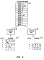
- the logic can track where in the pipeline instructions following a branch occur. For example, by noting that there was a branch in cycle 2, it is known that every stage following that, cycles 3-5 in this example, will have instructions along the branch predicted for instruction 6.
- the branch prediction logic will predict the branch direction (whether the branch is taken or not) and resolve the target address of the branch if it is predicted taken. If the direction or target address of this branch was mispredicted, the logic knows that all the instructions in cycles 3, 4 and 5, in the stages they are in at the appropriate time, need to be flushed. This could be done, for example, by setting all the valid bits corresponding to these instructions in an outstanding instruction FIFO to an invalid state.
- Dispatch unit 28 of the present invention provides instructions 1-4 in cycle 1, instructions 5-8 in cycle 2, and instructions 9-12 in cycle 3.
- the 12 instructions are dispatched in 3 cycles, as opposed to 5 cycles in the example of sequence 60.
- the 5 basic blocks of the prior art are combined into 3 superblocks. As can be seen, if there are a number of branches, this provides a significant throughput improvement.
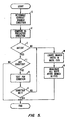
- branch resolution logic which is commonly implemented in the branch unit. This logic provides the actual input signal to change the valid bits in outstanding instruction FIFO 66. This type of logic has been used before to invalidate instruction groups following a group having a branch.
- the valid check logic 70 or 72 can match the instruction in the appropriate function unit with the appropriate instruction data in an outstanding instruction FIFO 66.
- Outstanding instruction FIFO 66 will always have the instructions in the program order, as shown by the numbers in Fig. 3. However, the order can be different in the function units since these may vary depending upon the type of instruction.
- the valid check logic can match the data in outstanding instruction FIFO 66 to the functional unit by examining the OP code (or encoded OP code), and knowing which function unit that corresponds to. Where multiple functional units which can perform the same type of OP code are active, the valid check logic has the same priority assignment logic as the dispatch unit. For instance, the first add instruction could always be sent to the first integer ALU for an integer add. In an alternate embodiment, a functional unit ID is put in the instruction FIFO when the instruction is issued.
- the dispatch unit only allows a single branch instruction in each cycle.
- instruction 4 would wait until the next cycle, with only three instructions being sent in the first cycle.
- This restriction is used to allow the usage'of only a single set of resolution hardware logic to determine the appropriate branch instruction. If there were a possibility of multiple branches within a single cycle, this logic would need to be duplicated, thus requiring more area on the microprocessor chip, so that the correct prediction of multiple branch instructions could be determined in a single cycle, or other short period of time (multiple cycles might be required for a very short cycle machine).
- the present invention could be embodied in other specific forms without departing from essential characteristics thereof.
- a tag could be carried along in the function unit instructions identifying a particular corresponding position in the outstanding instruction FIFO.
- other data storage structures could be used for storing the instruction validity data. Additional logic for checking the validity bits could be added to different areas of the pipeline. For instance, any time a long latency operation is about to commence (i.e., a floating point divide), the validity bit could be checked and the operation aborted if the instruction is now invalid.
Landscapes
- Engineering & Computer Science (AREA)
- Theoretical Computer Science (AREA)
- Software Systems (AREA)
- Physics & Mathematics (AREA)
- General Engineering & Computer Science (AREA)
- General Physics & Mathematics (AREA)
- Advance Control (AREA)
Claims (15)
- Microprocesseur comportant une pluralité d'unités fonctionnelles canalisées (32-46), au moins une mémoire tampon d'instructions (26), et une unité d'expédition d'instructions (28),
caractérisé en ce que
le microprocesseur comprend une mémoire FIFO d'instructions saillantes (66) stockant des données de poursuite pour chaque instruction dans la pluralité d'unités fonctionnelles canalisées (32-46), ces données de poursuite comprenant un bit de validité ;
l'unité d'expédition d'instructions est couplée entre la mémoire tampon d'instructions et la pluralité d'unités fonctionnelles canalisées ;
la mémoire tampon d'instructions au moins unique fournit un certain nombre d'instructions comprenant des instructions de ramification et des instructions cibles prédites ; et
l'unité d'expédition d'instructions est configurée pour expédier à la fois une instruction de ramification et une instruction cible prédite vers les unités fonctionnelles, en un cycle unique. - Microprocesseur selon la revendication 1,
comprenant en outre :une logique de prédiction de ramification (18) configurée pour comparer une direction de ramification prédite à une direction de ramification réelle, de façon que lorsqu'il existe une correspondance et lorsque la ramification est prise, on compare une adresse cible prédite à une adresse cible réelle ; etune logique de commande FIFO (71) configurée pour régler les bits valides dans un état invalide pour la poursuite des données correspondant à l'instruction cible et aux instructions suivantes dans la mémoire FIFO d'instructions saillantes, si la direction de ramification ou l'adresse cible prédite ont été mal prédites. - Microprocesseur selon la revendication 2,
comprenant en outre :une logique de validité de canalisation (32) configurée pour vérifier les bits de validité de chaque instruction à la fin des unités fonctionnelles canalisées, et pour empêcher le stockage de résultats d'opérations correspondant à une instruction quelconque ayant été déterminée comme étant invalide - Microprocesseur selon la revendication 2,
comprenant en outre :une logique de validité intermédiaire (70) configurée pour vérifier les bits de validité pour chaque instruction à un stade intermédiaire des unités canalisées avant une opération de latence longue des unités fonctionnelles, et pour empêcher l'opération de latence longue pour une instruction déterminée comme étant invalide. - Microprocesseur selon la revendication 4,
dans lequel
l'opération de latence longue est un accès en mémoire hors puce. - Microprocesseur selon la revendication 1,
dans lequel
l'unité d'expédition d'instructions est en outre configurée pour ne permettre qu'à une seule instruction de ramification d'être expédiée vers les unités fonctionnelles dans un cycle donné quelconque. - Microprocesseur selon la revendication 1,
dans lequel
l'unité d'expédition d'instructions est en outre configurée pour ne permettre qu'à un nombre prédéterminé d'instructions de ramification d'être expédiées vers les unités fonctionnelles dans un cycle donné quelconque. - Microprocesseur selon la revendication 7,
dans lequel
le nombre prédéterminé est égal à un. - Procédé pour faire fonctionner un microprocesseur comportant un certain nombre d'unités fonctionnelles canalisées (32-46), au moins une mémoire tampon d'instructions (26), et une unité d'expédition d'instructions (28),
comprenant les étapes consistant à :utiliser un élément pour fournir un certain nombre d'instructions à la mémoire tampon d'instructions, ces instructions comprenant des instructions de ramification et des instructions cibles prédites ;utiliser un élément provenant de la mémoire tampon d'instructions, pour expédier, avec cette unité d'expédition, à la fois une instruction de ramification et une instruction cible prédite, vers l'unité fonctionnelle et en un seul cycle ; etutiliser un élément pour stocker des données de poursuite pour chaque instruction située dans la pluralité d'unités fonctionnelles canalisées, dans une mémoire FIFO d'instructions saillantes, les données de poursuite comprenant un bit de validité. - Procédé selon la revendication 9,
comprenant en outre les étapes consistant à :utiliser un élément pour déterminer si l'instruction cible prédite a été correctement prédite ; etutiliser un élément pour régler les bits de validité dans un état invalide pour les données de poursuite correspondant à une instruction cible et à des instructions suivantes dans la mémoire FIFO d'instructions saillantes, si l'instruction cible prédite a été mal prédite. - Procédé selon la revendication 10,
comprenant en outre les étapes consistant à :utiliser un élément pour vérifier les bits de validité pour chaque instruction à la fin des unités fonctionnelles canalisées, dans la fin de la logique de validité de canalisation ; etutiliser un élément pour empêcher le stockage de résultats d'opérations correspondant à une instruction quelconque déterminée comme étant valide. - Procédé selon la revendication 10,
comprenant en outre les étapes consistant à :utiliser un élément pour vérifier les bits de validité pour chaque instruction, à un stade intermédiaire des unités canalisées, avant une opération de latence longue des unités fonctionnelles, dans une logique de validité intermédiaire ; etutiliser un élément pour empêcher l'opération de latence longue pour une instruction déterminée comme étant invalide. - Procédé selon la revendication 9,
comprenant en outre l'étape consistant à :utiliser un élément pour ne permettre qu'à un nombre prédéterminé d'instructions de ramification d'être expédiées vers les unités fonctionnelles par l'unité d'expédition d'instructions, dans un cycle donné quelconque. - Procédé selon la revendication 13,
dans lequel
le nombre prédéterminé est égal à un. - Système d'ordinateur comprenant :une mémoire et un microprocesseur couplé à cette mémoire, le microprocesseur étant tel que revendiqué dans l'une quelconque des revendications 1 à 8.
Applications Claiming Priority (2)
| Application Number | Priority Date | Filing Date | Title |
|---|---|---|---|
| US08/569,725 US5809324A (en) | 1995-12-07 | 1995-12-07 | Multiple instruction dispatch system for pipelined microprocessor without branch breaks |
| US569725 | 1995-12-07 |
Publications (3)
| Publication Number | Publication Date |
|---|---|
| EP0778519A2 EP0778519A2 (fr) | 1997-06-11 |
| EP0778519A3 EP0778519A3 (fr) | 1998-06-10 |
| EP0778519B1 true EP0778519B1 (fr) | 2003-02-19 |
Family
ID=24276603
Family Applications (1)
| Application Number | Title | Priority Date | Filing Date |
|---|---|---|---|
| EP96308514A Expired - Lifetime EP0778519B1 (fr) | 1995-12-07 | 1996-11-26 | Système à répartition des instructions multiples sans discontinuement de branchement dans un microprocesseur pipeliné |
Country Status (5)
| Country | Link |
|---|---|
| US (1) | US5809324A (fr) |
| EP (1) | EP0778519B1 (fr) |
| JP (1) | JP3779012B2 (fr) |
| KR (1) | KR100431975B1 (fr) |
| DE (1) | DE69626263T2 (fr) |
Families Citing this family (10)
| Publication number | Priority date | Publication date | Assignee | Title |
|---|---|---|---|---|
| US6289437B1 (en) * | 1997-08-27 | 2001-09-11 | International Business Machines Corporation | Data processing system and method for implementing an efficient out-of-order issue mechanism |
| US6289442B1 (en) * | 1998-10-05 | 2001-09-11 | Advanced Micro Devices, Inc. | Circuit and method for tagging and invalidating speculatively executed instructions |
| US6910123B1 (en) * | 2000-01-13 | 2005-06-21 | Texas Instruments Incorporated | Processor with conditional instruction execution based upon state of corresponding annul bit of annul code |
| US6976150B1 (en) * | 2000-04-06 | 2005-12-13 | The Board Of Governors For Higher Education, State Of Rhode Island And Providence Plantations | Resource flow computing device |
| US7072998B2 (en) * | 2003-05-13 | 2006-07-04 | Via Technologies, Inc. | Method and system for optimized FIFO full conduction control |
| US7636837B2 (en) | 2003-05-28 | 2009-12-22 | Fujitsu Limited | Apparatus and method for controlling instructions at time of failure of branch prediction |
| US7949861B2 (en) * | 2005-06-10 | 2011-05-24 | Qualcomm Incorporated | Method and apparatus for managing instruction flushing in a microprocessor's instruction pipeline |
| US8127115B2 (en) * | 2009-04-03 | 2012-02-28 | International Business Machines Corporation | Group formation with multiple taken branches per group |
| KR20130066402A (ko) * | 2011-12-12 | 2013-06-20 | 삼성전자주식회사 | 트레이스 데이터 저장 장치 및 방법 |
| US9122424B1 (en) * | 2013-07-18 | 2015-09-01 | Western Digital Technologies, Inc. | FIFO buffer clean-up |
Family Cites Families (6)
| Publication number | Priority date | Publication date | Assignee | Title |
|---|---|---|---|---|
| US4833599A (en) * | 1987-04-20 | 1989-05-23 | Multiflow Computer, Inc. | Hierarchical priority branch handling for parallel execution in a parallel processor |
| JP2845646B2 (ja) * | 1990-09-05 | 1999-01-13 | 株式会社東芝 | 並列演算処理装置 |
| US5493669A (en) * | 1993-03-03 | 1996-02-20 | Motorola, Inc. | Data processor for simultaneously searching two fields of the rename buffer having first and second most recently allogated bits |
| US5644779A (en) * | 1994-04-15 | 1997-07-01 | International Business Machines Corporation | Processing system and method of operation for concurrent processing of branch instructions with cancelling of processing of a branch instruction |
| US5542109A (en) * | 1994-08-31 | 1996-07-30 | Exponential Technology, Inc. | Address tracking and branch resolution in a processor with multiple execution pipelines and instruction stream discontinuities |
| US5598546A (en) * | 1994-08-31 | 1997-01-28 | Exponential Technology, Inc. | Dual-architecture super-scalar pipeline |
-
1995
- 1995-12-07 US US08/569,725 patent/US5809324A/en not_active Expired - Lifetime
-
1996
- 1996-11-26 DE DE69626263T patent/DE69626263T2/de not_active Expired - Fee Related
- 1996-11-26 EP EP96308514A patent/EP0778519B1/fr not_active Expired - Lifetime
- 1996-12-04 KR KR1019960061584A patent/KR100431975B1/ko not_active IP Right Cessation
- 1996-12-05 JP JP33912596A patent/JP3779012B2/ja not_active Expired - Lifetime
Also Published As
| Publication number | Publication date |
|---|---|
| JPH09274565A (ja) | 1997-10-21 |
| KR100431975B1 (ko) | 2004-10-28 |
| KR970049478A (ko) | 1997-07-29 |
| US5809324A (en) | 1998-09-15 |
| DE69626263D1 (de) | 2003-03-27 |
| DE69626263T2 (de) | 2004-02-05 |
| JP3779012B2 (ja) | 2006-05-24 |
| EP0778519A2 (fr) | 1997-06-11 |
| EP0778519A3 (fr) | 1998-06-10 |
Similar Documents
| Publication | Publication Date | Title |
|---|---|---|
| US6122656A (en) | Processor configured to map logical register numbers to physical register numbers using virtual register numbers | |
| US5553256A (en) | Apparatus for pipeline streamlining where resources are immediate or certainly retired | |
| US6119223A (en) | Map unit having rapid misprediction recovery | |
| US5067069A (en) | Control of multiple functional units with parallel operation in a microcoded execution unit | |
| US5903750A (en) | Dynamic branch prediction for branch instructions with multiple targets | |
| US6065115A (en) | Processor and method for speculatively executing instructions from multiple instruction streams indicated by a branch instruction | |
| US6260138B1 (en) | Method and apparatus for branch instruction processing in a processor | |
| US5584009A (en) | System and method of retiring store data from a write buffer | |
| US5761476A (en) | Non-clocked early read for back-to-back scheduling of instructions | |
| US6079014A (en) | Processor that redirects an instruction fetch pipeline immediately upon detection of a mispredicted branch while committing prior instructions to an architectural state | |
| US5611063A (en) | Method for executing speculative load instructions in high-performance processors | |
| JP3597540B2 (ja) | 並列データプロセッサにおけるアクティブ命令を回転させる方法および装置 | |
| CN113535423A (zh) | 具有在预置未来时间执行指令的流水线控制的微处理器 | |
| JPH07334364A (ja) | スーパースカラマイクロプロセッサおよびropを処理する方法 | |
| US6393550B1 (en) | Method and apparatus for pipeline streamlining where resources are immediate or certainly retired | |
| US5684971A (en) | Reservation station with a pseudo-FIFO circuit for scheduling dispatch of instructions | |
| US5740398A (en) | Program order sequencing of data in a microprocessor with write buffer | |
| EP0651331B1 (fr) | Tampon d'écriture pour un microprocesseur superscalaire à pipeline | |
| US5778248A (en) | Fast microprocessor stage bypass logic enable | |
| EP1099158B1 (fr) | Processeur configure pour liberer selectivement des registres physiques sur retrait d'instructions | |
| US5727177A (en) | Reorder buffer circuit accommodating special instructions operating on odd-width results | |
| EP0778519B1 (fr) | Système à répartition des instructions multiples sans discontinuement de branchement dans un microprocesseur pipeliné | |
| JP3794918B2 (ja) | 復帰選択ビットを用いて分岐予測のタイプを分類する分岐予測 | |
| US6101597A (en) | Method and apparatus for maximum throughput scheduling of dependent operations in a pipelined processor | |
| US5778247A (en) | Multi-pipeline microprocessor with data precision mode indicator |
Legal Events
| Date | Code | Title | Description |
|---|---|---|---|
| PUAI | Public reference made under article 153(3) epc to a published international application that has entered the european phase |
Free format text: ORIGINAL CODE: 0009012 |
|
| AK | Designated contracting states |
Kind code of ref document: A2 Designated state(s): DE GB SE |
|
| PUAL | Search report despatched |
Free format text: ORIGINAL CODE: 0009013 |
|
| AK | Designated contracting states |
Kind code of ref document: A3 Designated state(s): DE GB SE |
|
| 17P | Request for examination filed |
Effective date: 19980803 |
|
| 17Q | First examination report despatched |
Effective date: 20011001 |
|
| GRAH | Despatch of communication of intention to grant a patent |
Free format text: ORIGINAL CODE: EPIDOS IGRA |
|
| GRAH | Despatch of communication of intention to grant a patent |
Free format text: ORIGINAL CODE: EPIDOS IGRA |
|
| GRAA | (expected) grant |
Free format text: ORIGINAL CODE: 0009210 |
|
| AK | Designated contracting states |
Designated state(s): DE GB SE |
|
| REG | Reference to a national code |
Ref country code: GB Ref legal event code: FG4D |
|
| REF | Corresponds to: |
Ref document number: 69626263 Country of ref document: DE Date of ref document: 20030327 Kind code of ref document: P |
|
| PG25 | Lapsed in a contracting state [announced via postgrant information from national office to epo] |
Ref country code: SE Free format text: LAPSE BECAUSE OF FAILURE TO SUBMIT A TRANSLATION OF THE DESCRIPTION OR TO PAY THE FEE WITHIN THE PRESCRIBED TIME-LIMIT Effective date: 20030519 |
|
| RAP2 | Party data changed (patent owner data changed or rights of a patent transferred) |
Owner name: SUN MICROSYSTEMS, INC. |
|
| PLBE | No opposition filed within time limit |
Free format text: ORIGINAL CODE: 0009261 |
|
| STAA | Information on the status of an ep patent application or granted ep patent |
Free format text: STATUS: NO OPPOSITION FILED WITHIN TIME LIMIT |
|
| 26N | No opposition filed |
Effective date: 20031120 |
|
| PGFP | Annual fee paid to national office [announced via postgrant information from national office to epo] |
Ref country code: DE Payment date: 20061123 Year of fee payment: 11 |
|
| PG25 | Lapsed in a contracting state [announced via postgrant information from national office to epo] |
Ref country code: DE Free format text: LAPSE BECAUSE OF NON-PAYMENT OF DUE FEES Effective date: 20080603 |
|
| PGFP | Annual fee paid to national office [announced via postgrant information from national office to epo] |
Ref country code: GB Payment date: 20151125 Year of fee payment: 20 |
|
| REG | Reference to a national code |
Ref country code: GB Ref legal event code: PE20 Expiry date: 20161125 |
|
| PG25 | Lapsed in a contracting state [announced via postgrant information from national office to epo] |
Ref country code: GB Free format text: LAPSE BECAUSE OF EXPIRATION OF PROTECTION Effective date: 20161125 |