EP0777367A1 - Apparatus for cancelling signal dispersion in communications systems - Google Patents
Apparatus for cancelling signal dispersion in communications systems Download PDFInfo
- Publication number
- EP0777367A1 EP0777367A1 EP96410118A EP96410118A EP0777367A1 EP 0777367 A1 EP0777367 A1 EP 0777367A1 EP 96410118 A EP96410118 A EP 96410118A EP 96410118 A EP96410118 A EP 96410118A EP 0777367 A1 EP0777367 A1 EP 0777367A1
- Authority
- EP
- European Patent Office
- Prior art keywords
- packet
- bits
- parallel
- circuit
- transmission
- Prior art date
- Legal status (The legal status is an assumption and is not a legal conclusion. Google has not performed a legal analysis and makes no representation as to the accuracy of the status listed.)
- Withdrawn
Links
Images

Classifications
-
- H—ELECTRICITY
- H04—ELECTRIC COMMUNICATION TECHNIQUE
- H04L—TRANSMISSION OF DIGITAL INFORMATION, e.g. TELEGRAPHIC COMMUNICATION
- H04L25/00—Baseband systems
- H04L25/02—Details ; arrangements for supplying electrical power along data transmission lines
- H04L25/03—Shaping networks in transmitter or receiver, e.g. adaptive shaping networks
- H04L25/03828—Arrangements for spectral shaping; Arrangements for providing signals with specified spectral properties
- H04L25/03866—Arrangements for spectral shaping; Arrangements for providing signals with specified spectral properties using scrambling
Definitions
- the present invention relates to a data processing chain, intended to reduce the number of errors in a transmission.
- the invention relates more particularly to one of the elements of the chain, which is a dispersion suppression circuit also called "descrambling" circuit.
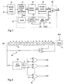
- FIG. 1 represents an example of a processing chain used at the level of a receiver conforming to the European standard for the transmission of digital television signals by satellite.
- digital data is transmitted in byte packets, generally 204 byte packets of which 16 bytes are redundant and are used for error correction. Packet limits are determined by synchronization codes.
- Each packet undergoes a dispersion or "interference" on transmission which serves to reduce the frequency spectrum of the transmission signal in order to facilitate its processing.
- the dispersion consists in combining the bits of each packet by OR-exclusive with corresponding bits supplied by a polynomial counter initialized to an adequate value.
- Each packet also undergoes external coding (Reed-Solomon coding) which generates the aforementioned redundant bytes in order to be able to correct several errors in each packet.
- external coding Random-Solomon coding
- each packet is interleaved in order to better correct bursts of consecutive errors. Indeed, if several consecutive errors occur in the transmission, when the data will have been deinterleaved, the errors of this burst will be in isolated locations and are therefore easier to correct.
- bits to be transmitted undergo internal coding (convolutional coding) to create two redundant transmission signals I and Q which will also be used to reduce the number of errors.
- FIG. 1 represents a part of the architecture according to the aforementioned European standard of the chain of reverse processing of the I and Q signals, on reception.
- the received I and Q signals undergo internal decoding (using the Viterbi algorithm).
- the decoder 10 In the serial signal produced by the decoder 10, synchronization words used to delimit the packets are detected and a series-parallel conversion is carried out to supply bytes.
- deinterlacing In consecutive blocks 14, 16 and 18, deinterlacing, external decoding and dispersion suppression are carried out respectively.
- FIG. 1 the architecture of Figure 1 operates at two different frequencies.
- a first part that is to say the internal decoding circuit 10 and a part of the series-parallel synchronization and conversion circuit 12, are clocked by a fast clock CK at the bit transmission frequency, while the rest of the architecture is clocked by a slower clock CK / 8 at the transmission frequency of the bytes.
- the transmission frequency of the bits is at the limit of what can be obtained with current technologies.
- circuits that operate at this frequency must be made with special care to minimize the clock front delays and to compensate for these delays to work around timing issues. These problems are not encountered in other circuits operating at lower frequencies (CK / 8).
- FIG. 2 represents a conventional dispersion suppression circuit.
- This circuit comprises a polynomial counter consisting of a shift register 20 whose input receives an OR-exclusive combination 22 of the output of the shift register and one or more intermediate flip-flops of this shift register.
- the shift register 20 is clocked by the bit clock CK and receives an initial value at the start of each group of eight packets to be processed. The start of the packet group is determined by a SYNC group synchronization signal.
- the shift register 20 comprises fifteen flip-flops and the input of the register receives the combination by OR-exclusive of the outputs of the last and penultimate flip-flops.
- the initialization value is 100101010000000.
- the output of the OR-exclusive gate 22, constituting the output of the polynomial counter, provides correction bits c to a first input of an OR-exclusive gate 24, at the rate of transmission of the bits.
- B bits of "scrambled" packets are supplied to a second input of gate 24.
- the output of this gate 24 provides bits b 'of "unscrambled" packets.
- the circuit of FIG. 2, particularly simple, is intended to operate on a serial transmission of bits b.
- the dispersion suppression circuit 18 of the architecture of FIG. 1 must work on a parallel transmission of bytes. For this, two solutions could be envisaged.
- a first solution consists in using a parallel arithmetic operating on bytes.
- the resulting circuit, of parallel structure would be complex and would occupy a significant surface compared to the series circuit of figure 2.
- a second solution consists in performing a parallel-series conversion at the output of the external decoder 16 in order to be able to use at 18 the serial circuit of FIG. 2, then to reconvert in parallel the bits supplied in series by the circuit of FIG. 2. If the transmission speed of the bits was slow, this solution would be much less complex than the first solution mentioned above. However, it is always difficult, in any circuit, to pass from a low operating frequency (at the parallel output of the external decoder 16) to a high operating frequency (at the serial input of the circuit of FIG. 2) . The high frequency of the circuit of FIG. 2 must be synchronized with the lower frequency of the decoder 16. This synchronization does not pose any particular problem if the high frequency is far from the technological limits. However, if this high frequency is at the limit of what technology accepts, synchronization becomes particularly delicate and requires the use of complex solutions. In addition, synchronization solutions that will work well in one technology will not necessarily work in another technology.
- An object of the present invention is to provide a dispersion suppression circuit operating in parallel which is of particularly simple structure and which can operate at the limit frequency of the technology employed.
- the present invention provides for performing a series-parallel conversion of the correction bits supplied by a serial polynomial counter.
- the correction bits are therefore supplied by bytes by the serial-parallel converter and can be combined with the bytes of the packet by eight OR-exclusive gates.
- the present invention more particularly provides a dispersion suppression circuit in a transmission of a data packet, comprising a polynomial counter supplying, at the transmission rate of the bits of the packet, correction bits to be combined respectively with the bits of the packet by OU-exclusive.
- the correction bits are supplied to a serial-parallel converter whose output is combined with successive words transmitted in parallel from the packet.
- the polynomial counter is initialized at the start of a packet.
- the dispersion suppression circuit is used in a packet processing chain downstream of a packet synchronization word detection and of a serial-parallel conversion of the transmission of the bits of the packet, the polynomial counter receiving a delayed initialization signal, with respect to a synchronization detection, of the offset between a synchronization detection and the appearance of the start of a packet at the input of the suppression circuit.
- FIG. 3 represents a data processing chain which comprises the same elements as that of FIG. 1, designated by the same references.
- the bytes leaving the external decoder 16 are supplied to a dispersion suppression circuit 18 'according to the present invention.
- This dispersion suppression circuit 18 ′ comprises a series polynomial counter 26, of the type of that of FIG. 2, supplying correction bits c at the bit transmission frequency (CK).
- CK bit transmission frequency
- These correction bits c are supplied to a serial-parallel converter 28 which reconstructs, from bits c, correction bytes C at the rate (CK / 8) of the bytes supplied by the decoder 16.
- These correction bytes C are combined by OR-exclusive in 30 to the bytes leaving the decoder 16.
- the "unscrambled" bytes are formed by the results of these combinations in 30.
- the polynomial counter 26 must be initialized in synchronism with the arrival at the output of the external decoder 16 of the packet starts.
- the packet starts are detected by the synchronization detector 12 which activates a SYNC signal on each detection of a synchronization word defining a packet start.
- This SYNC signal is used to initialize the polynomial counter 26, and is supplied to it via a circuit 32 which delays the SYNC signal so as to initialize the polynomial counter 26 in correspondence with the appearance of the start of a group. of eight packets at the output of the external decoder 16.
- the serial-parallel converter 28 must provide the corresponding correction byte C.
- the polynomial counter 26 must have been initialized eight cycles of the clock bit CK earlier.
- a parallel dispersion suppression circuit according to the present invention occupies an area comparable to that occupied by the series circuit of FIG. 2.
- a parallel-series converter is not used which, as explained above, has huge problems with switching from a slow frequency (byte frequency) to a fast frequency (bit frequency) at the limit of what the technology used accepts.
- a time base which comprises a packet counter initialized by the synchronization circuit 12 at each start of a group of eight packets, and a counter d bytes initialized by the synchronization circuit 12 at each start of a packet.
- the packet counter indicates the rank of a current packet in the current group
- the byte counter indicates the rank of a current byte in the current packet (a current byte being that provided by the serial converter - parallel 12).
- Delay 32 is then obtained while waiting for the packet and byte counters to reach corresponding values.
- the packets to be processed comprise 204 bytes and the delay introduced by blocks 14 and 16 is 1157 bytes.
- the polynomial counter 28 is initialized when the packet and byte counters reach the value 5 and the value 136, respectively.
- FIG. 4 represents a detailed embodiment of the dispersion suppression circuit 18 '.
- the polynomial counter 26, comprising a shift register 20 and an OR-exclusive gate 22, is identical to that of FIG. 2.
- the shift register 20 is clocked by the bit clock CK and it is initialized via the delay circuit 32.
- the output of the OR-exclusive gate 22, delivering in series correction bits c, is supplied to the serial-parallel converter 28.
- Each of eight OR-exclusive gates 30 receives a bit corresponding to "scrambled" bytes "and a corresponding bit of the correction byte C supplied by the parallel serial converter 28.
- the outputs of the OR-exclusive gates 30 supply the bits b 'of each of the" unscrambled "bytes.
Abstract
Description
La présente invention concerne une chaîne de traitement de données, destinée à réduire le nombre d'erreurs dans une transmission. L'invention concerne plus particulièrement l'un des éléments de la chaîne, qui est un circuit de suppression de dispersion aussi appelé circuit de "débrouillage".The present invention relates to a data processing chain, intended to reduce the number of errors in a transmission. The invention relates more particularly to one of the elements of the chain, which is a dispersion suppression circuit also called "descrambling" circuit.
La figure 1 représente un exemple de chaîne de traitement utilisée au niveau d'un récepteur conforme à la norme européenne de transmission de signaux de télévision numérique par satellite. Selon cette norme, les données numériques sont transmises par paquets d'octets, généralement des paquets de 204 octets dont 16 octets sont redondants et servent à une correction d'erreur. Les limites des paquets sont déterminées par des codes de synchronisation.FIG. 1 represents an example of a processing chain used at the level of a receiver conforming to the European standard for the transmission of digital television signals by satellite. According to this standard, digital data is transmitted in byte packets, generally 204 byte packets of which 16 bytes are redundant and are used for error correction. Packet limits are determined by synchronization codes.
Chaque paquet subit à l'émission une dispersion ou "brouillage" qui sert à réduire le spectre de fréquence du signal de transmission afin de faciliter son traitement. La dispersion consiste à combiner les bits de chaque paquet par OU-exclusif avec des bits correspondants fournis par un compteur polynomial initialisé à une valeur adéquate.Each packet undergoes a dispersion or "interference" on transmission which serves to reduce the frequency spectrum of the transmission signal in order to facilitate its processing. The dispersion consists in combining the bits of each packet by OR-exclusive with corresponding bits supplied by a polynomial counter initialized to an adequate value.
Chaque paquet subit également un codage externe (codage Reed-Solomon) qui génère les octets redondants susmentionnés pour pouvoir corriger plusieurs erreurs dans chaque paquet.Each packet also undergoes external coding (Reed-Solomon coding) which generates the aforementioned redundant bytes in order to be able to correct several errors in each packet.
Les octets de chaque paquet sont entrelacés afin de pouvoir mieux corriger des salves d'erreurs consécutives. En effet, si plusieurs erreurs consécutives se produisent dans la transmission, lorsque les données auront été désentrelacées, les erreurs de cette salve se trouveront à des emplacements isolés et sont donc plus faciles à corriger.The bytes of each packet are interleaved in order to better correct bursts of consecutive errors. Indeed, if several consecutive errors occur in the transmission, when the data will have been deinterleaved, the errors of this burst will be in isolated locations and are therefore easier to correct.
Finalement, les bits à transmettre subissent un codage interne (codage convolutif) pour créer deux signaux de transmission redondants I et Q qui serviront également à réduire le nombre d'erreurs.Finally, the bits to be transmitted undergo internal coding (convolutional coding) to create two redundant transmission signals I and Q which will also be used to reduce the number of errors.
La figure 1 représente une partie de l'architecture selon la norme européenne susmentionnée de la chaîne de traitement inverse des signaux I et Q, à la réception. En 10, les signaux I et Q reçus subissent un décodage interne (utilisant l'algorithme de Viterbi). En 12, dans le signal série produit par le décodeur 10, on détecte des mots de synchronisation servant à délimiter les paquets et on effectue une conversion série-parallèle pour fournir des octets. Dans des blocs consécutifs 14, 16 et 18, on effectue respectivement le désentrelacement, le décodage externe, et la suppression de dispersion.FIG. 1 represents a part of the architecture according to the aforementioned European standard of the chain of reverse processing of the I and Q signals, on reception. At 10, the received I and Q signals undergo internal decoding (using the Viterbi algorithm). At 12, in the serial signal produced by the
On remarque que l'architecture de la figure 1 fonctionne à deux fréquences différentes. Une première partie, c'est-à-dire le circuit de décodage interne 10 et une partie du circuit 12 de synchronisation et de conversion série-parallèle, sont cadencées par une horloge rapide CK à la fréquence de transmission des bits, tandis que le reste de l'architecture est cadencé par une horloge plus lente CK/8 à la fréquence de transmission des octets.Note that the architecture of Figure 1 operates at two different frequencies. A first part, that is to say the
Généralement, la fréquence de transmission des bits est à la limite de ce que l'on peut obtenir avec les technologies courantes. Ainsi, les circuits qui fonctionnent à cette fréquence doivent être réalisés avec un soin particulier pour minimiser les retards de front d'horloge et pour compenser ces retards afin de contourner des problèmes de synchronisation. On ne rencontre pas ces problèmes dans les autres circuits fonctionnant à fréquence plus basse (CK/8).Generally, the transmission frequency of the bits is at the limit of what can be obtained with current technologies. Thus, circuits that operate at this frequency must be made with special care to minimize the clock front delays and to compensate for these delays to work around timing issues. These problems are not encountered in other circuits operating at lower frequencies (CK / 8).
La figure 2 représente un circuit classique de suppression de dispersion. Ce circuit comprend un compteur polynomial constitué d'un registre à décalage 20 dont l'entrée reçoit une combinaison par OU-exclusif 22 de la sortie du registre à décalage et d'une ou plusieurs bascules intermédiaires de ce registre à décalage. Le registre à décalage 20 est cadencé par l'horloge bit CK et reçoit une valeur initiale au début de chaque groupe de huit paquets à traiter. Le début du groupe de paquets est déterminé par un signal de synchronisation de groupe SYNC. Dans le cadre de la norme européenne susmentionnée, le registre à décalage 20 comporte quinze bascules et l'entrée du registre reçoit la combinaison par OU-exclusif des sorties des dernière et avant dernière bascules. La valeur d'initialisation est 100101010000000.FIG. 2 represents a conventional dispersion suppression circuit. This circuit comprises a polynomial counter consisting of a
La sortie de la porte OU-exclusif 22, constituant la sortie du compteur polynomial, fournit des bits de correction c à une première entrée d'une porte OU-exclusif 24, à la cadence de transmission des bits. Les bits b des paquets "brouillés" sont fournis à une deuxième entrée de la porte 24. La sortie de cette porte 24 fournit les bits b' des paquets "débrouillés".The output of the OR-exclusive gate 22, constituting the output of the polynomial counter, provides correction bits c to a first input of an OR-
Le circuit de la figure 2, particulièrement simple, est destiné à fonctionner sur une transmission série de bits b. Or, le circuit de suppression de dispersion 18 de l'architecture de la figure 1 doit travailler sur une transmission parallèle d'octets. Pour cela, deux solutions pourraient être envisagées.The circuit of FIG. 2, particularly simple, is intended to operate on a serial transmission of bits b. However, the
Une première solution consiste à utiliser une arithmétique parallèle opérant sur des octets. Le circuit résultant, de structure parallèle, serait complexe et occuperait une surface notable par rapport au circuit série de la figure 2.A first solution consists in using a parallel arithmetic operating on bytes. The resulting circuit, of parallel structure, would be complex and would occupy a significant surface compared to the series circuit of figure 2.
Une deuxième solution consiste à effectuer une conversion parallèle-série à la sortie du décodeur externe 16 afin de pouvoir utiliser en 18 le circuit série de la figure 2, puis à reconvertir en parallèle les bits fournis en série par le circuit de la figure 2. Si la vitesse de transmission des bits était lente, cette solution serait nettement moins complexe que la première solution susmentionnée. Toutefois, il est toujours délicat, dans un circuit quelconque, de passer d'une fréquence de fonctionnement basse (à la sortie parallèle du décodeur externe 16) à une fréquence de fonctionnement élevée (à l'entrée série du circuit de la figure 2). La fréquence élevée du circuit de la figure 2 doit être synchronisée sur la fréquence plus basse du décodeur 16. Cette synchronisation ne pose pas de problème particulier si la fréquence élevée est loin des limites technologiques. Toutefois, si cette fréquence élevée est à la limite de ce qu'accepte la technologie, la synchronisation devient particulièrement délicate et nécessite l'emploi de solutions complexes. De plus, les solutions de synchronisation qui fonctionneront bien dans une certaine technologie ne fonctionneront pas nécessairement dans une autre technologie.A second solution consists in performing a parallel-series conversion at the output of the
Par contre, une conversion série-parallèle, telle qu'effectuée en 12 à la figure 1, ne pose aucun problème.On the other hand, a series-parallel conversion, as carried out at 12 in FIG. 1, poses no problem.
Un objet de la présente invention est de prévoir un circuit de suppression de dispersion fonctionnant en parallèle qui soit de structure particulièrement simple et qui puisse fonctionner à la fréquence limite de la technologie employée.An object of the present invention is to provide a dispersion suppression circuit operating in parallel which is of particularly simple structure and which can operate at the limit frequency of the technology employed.
Pour atteindre cet objet, la présente invention prévoit d'effectuer une conversion série-parallèle des bits de correction fournis par un compteur polynomial série. Les bits de correction sont donc fournis par octets par le convertisseur série-parallèle et peuvent être combinés aux octets du paquet par huit portes OU-exclusif.To achieve this object, the present invention provides for performing a series-parallel conversion of the correction bits supplied by a serial polynomial counter. The correction bits are therefore supplied by bytes by the serial-parallel converter and can be combined with the bytes of the packet by eight OR-exclusive gates.
Avec cette configuration, on évite le passage d'une fréquence basse à une fréquence élevée (comme dans un convertisseur parallèle-série), qui pose des problèmes de synchronisation.With this configuration, the passage from a low frequency to a high frequency is avoided (as in a parallel-series converter), which poses synchronization problems.
La présente invention prévoit plus particulièrement un circuit de suppression de dispersion dans une transmission d'un paquet de données, comprenant un compteur polynomial fournissant, à la cadence de transmission des bits du paquet, des bits de correction à combiner respectivement aux bits du paquet par OU-exclusif. Les bits de correction sont fournis à un convertisseur série-parallèle dont la sortie est combinée aux mots successifs transmis en parallèle du paquet.The present invention more particularly provides a dispersion suppression circuit in a transmission of a data packet, comprising a polynomial counter supplying, at the transmission rate of the bits of the packet, correction bits to be combined respectively with the bits of the packet by OU-exclusive. The correction bits are supplied to a serial-parallel converter whose output is combined with successive words transmitted in parallel from the packet.
Selon un mode de réalisation de l'invention, le compteur polynomial est initialisé au début d'un paquet.According to one embodiment of the invention, the polynomial counter is initialized at the start of a packet.
Selon un mode de réalisation de l'invention, le circuit de suppression de dispersion est utilisé dans une chaîne de traitement du paquet en aval d'une détection de mot de synchronisation du paquet et d'une conversion série-parallèle de la transmission des bits du paquet, le compteur polynomial recevant un signal d'initialisation retardé, par rapport à une détection de synchronisation, du décalage entre une détection de synchronisation et l'apparition du début d'un paquet à l'entrée du circuit de suppression.According to one embodiment of the invention, the dispersion suppression circuit is used in a packet processing chain downstream of a packet synchronization word detection and of a serial-parallel conversion of the transmission of the bits of the packet, the polynomial counter receiving a delayed initialization signal, with respect to a synchronization detection, of the offset between a synchronization detection and the appearance of the start of a packet at the input of the suppression circuit.
Ces objets, caractéristiques et avantages, ainsi que d'autres de la présente invention seront exposés en détail dans la description suivante de modes de réalisation particuliers faite à titre non-limitatif en relation avec les figures jointes parmi lesquelles :
- les figures 1 et 2, précédemment décrites, illustrent l'état de la technique et le problème que vise à résoudre la présente invention ;
- la figure 3 représente une architecture d'une chaîne de traitement de données classique dans laquelle est incorporé un circuit de suppression de dispersion selon la présente invention ; et
- la figure 4 représente un mode de réalisation détaillé d'un circuit de suppression de dispersion selon la présente invention.
- Figures 1 and 2, previously described, illustrate the state of the art and the problem which the present invention seeks to solve;
- FIG. 3 represents an architecture of a conventional data processing chain in which a dispersion suppression circuit according to the present invention is incorporated; and
- FIG. 4 represents a detailed embodiment of a dispersion suppression circuit according to the present invention.
La figure 3 représente une chaîne de traitement de données qui comprend des mêmes éléments que celle de la figure 1, désignés par des mêmes références. Les octets sortant du décodeur externe 16 sont fournis à un circuit de suppression de dispersion 18' selon la présente invention. Ce circuit de suppression de dispersion 18' comprend un compteur polynomial série 26, du type de celui de la figure 2, fournissant des bits de correction c à la fréquence de transmission des bits (CK). Ces bits de correction c sont fournis à un convertisseur série-parallèle 28 qui reconstitue, à partir des bits c, des octets de correction C à la cadence (CK/8) des octets fournis par le décodeur 16. Ces octets de correction C sont combinés par OU-exclusif en 30 aux octets sortant du décodeur 16. Les octets "débrouillés" sont constitués par les résultats de ces combinaisons en 30.FIG. 3 represents a data processing chain which comprises the same elements as that of FIG. 1, designated by the same references. The bytes leaving the
Bien entendu, le compteur polynomial 26 doit être initialisé en synchronisme avec l'arrivée à la sortie du décodeur externe 16 des débuts de paquet. Les débuts de paquet sont détectés par le détecteur de synchronisation 12 qui active un signal SYNC à chaque détection d'un mot de synchronisation définissant un début de paquet. Ce signal SYNC est utilisé pour initialiser le compteur polynomial 26, et lui est fourni par l'intermédiaire d'un circuit 32 qui retarde le signal SYNC de manière à initialiser le compteur polynomial 26 en correspondance avec l'apparition du début d'un groupe de huit paquets à la sortie du décodeur externe 16. Lorsque le premier octet d'un paquet apparaît à la sortie du décodeur 16, le convertisseur série-parallèle 28 doit fournir l'octet de correction C correspondant. Pour cela, le compteur polynomial 26 doit avoir été initialisé huit cycles de l'horloge bit CK plus tôt.Of course, the
Un circuit parallèle de suppression de dispersion selon la présente invention occupe une surface comparable à celle occupée par le circuit série de la figure 2. De plus, on n'utilise pas de convertisseur parallèle-série qui, comme cela a été expliqué précédemment, présente d'énormes problèmes liés au fait du passage d'une fréquence lente (fréquence octet) à une fréquence rapide (fréquence bit) à la limite de ce qu'accepte la technologie employée.A parallel dispersion suppression circuit according to the present invention occupies an area comparable to that occupied by the series circuit of FIG. 2. In addition, a parallel-series converter is not used which, as explained above, has huge problems with switching from a slow frequency (byte frequency) to a fast frequency (bit frequency) at the limit of what the technology used accepts.
Généralement, pour synchroniser les divers circuits de l'architecture de la figure 1, on prévoit une base de temps qui comporte un compteur de paquets initialisé par le circuit de synchronisation 12 à chaque début d'un groupe de huit paquets, et un compteur d'octets initialisé par le circuit de synchronisation 12 à chaque début d'un paquet. Ainsi, le compteur de paquets indique le rang d'un paquet courant dans le groupe courant, et le compteur d'octets indique le rang d'un octet courant dans le paquet courant (un octet courant étant celui qui est fourni par le convertisseur série-parallèle 12).Generally, to synchronize the various circuits of the architecture of FIG. 1, a time base is provided which comprises a packet counter initialized by the
On obtient alors le retard 32 en attendant que les compteurs de paquets et d'octets atteignent des valeurs correspondantes.
Dans le cadre de la norme européenne susmentionnée, les paquets à traiter comportent 204 octets et le retard introduit par les blocs 14 et 16 est de 1157 octets. Dans cet exemple, le compteur polynomial 28 est initialisé quand les compteurs de paquets et d'octets atteignent respectivement la valeur 5 et la valeur 136.In the context of the above-mentioned European standard, the packets to be processed comprise 204 bytes and the delay introduced by
La figure 4 représente un mode de réalisation détaillé du circuit de suppression de dispersion 18'. Le compteur polynomial 26, comportant un registre à décalage 20 et une porte OU-exclusif 22, est identique à celui de la figure 2. Le registre à décalage 20 est cadencé par l'horloge bit CK et il est initialisé par l'intermédiaire du circuit de retard 32. La sortie de la porte OU-exclusif 22, délivrant en série des bits de correction c, est fournie au convertisseur série-parallèle 28. Chacune de huit portes OU-exclusif 30 reçoit un bit correspondant b des octets "brouillés" et un bit correspondant de l'octet de correction C fourni par le convertisseur série parallèle 28. Les sorties des portes OU-exclusif 30 fournissent les bits b' de chacun des octets "débrouillés".FIG. 4 represents a detailed embodiment of the dispersion suppression circuit 18 '. The
La présente invention a été décrite dans le cadre du traitement d'une transmission selon une norme particulière, mais il est clair que le circuit de suppression de dispersion selon l'invention s'applique à toute chaîne de traitement parallèle.The present invention has been described in the context of the processing of a transmission according to a particular standard, but it is clear that the dispersion suppression circuit according to the invention applies to any parallel processing chain.
Claims (3)
Applications Claiming Priority (2)
| Application Number | Priority Date | Filing Date | Title |
|---|---|---|---|
| FR9514383 | 1995-11-30 | ||
| FR9514383A FR2742016B1 (en) | 1995-11-30 | 1995-11-30 | CIRCUIT FOR SUPPRESSING DISPERSION IN DATA TRANSMISSION |
Publications (1)
| Publication Number | Publication Date |
|---|---|
| EP0777367A1 true EP0777367A1 (en) | 1997-06-04 |
Family
ID=9485173
Family Applications (1)
| Application Number | Title | Priority Date | Filing Date |
|---|---|---|---|
| EP96410118A Withdrawn EP0777367A1 (en) | 1995-11-30 | 1996-11-22 | Apparatus for cancelling signal dispersion in communications systems |
Country Status (3)
| Country | Link |
|---|---|
| US (1) | US5784013A (en) |
| EP (1) | EP0777367A1 (en) |
| FR (1) | FR2742016B1 (en) |
Families Citing this family (3)
| Publication number | Priority date | Publication date | Assignee | Title |
|---|---|---|---|---|
| KR100219481B1 (en) * | 1996-05-23 | 1999-09-01 | 윤종용 | Descrambling data generating method and device of a cd-rom decoder and descrambler thereby |
| US6636607B1 (en) * | 1998-10-08 | 2003-10-21 | Ati International Srl | Method and apparatus for controlling display of content signals |
| US6976265B1 (en) | 1998-10-08 | 2005-12-13 | Ati International Srl | Method and apparatus for controlling display of content signals |
Citations (4)
| Publication number | Priority date | Publication date | Assignee | Title |
|---|---|---|---|---|
| EP0488325A2 (en) * | 1990-11-28 | 1992-06-03 | Siemens Aktiengesellschaft | Parallel scrambler used in sonet data transmission |
| EP0549047A1 (en) * | 1991-12-20 | 1993-06-30 | Koninklijke KPN N.V. | Scrambler/descrambler and synchronizer for a data transmission system |
| US5241602A (en) * | 1992-02-07 | 1993-08-31 | Byeong Gi Lee | Parallel scrambling system |
| EP0566330A2 (en) * | 1992-04-16 | 1993-10-20 | AT&T Corp. | Multilevel coding using trellis-coded modulation and reed-solomon codes |
Family Cites Families (1)
| Publication number | Priority date | Publication date | Assignee | Title |
|---|---|---|---|---|
| US5185799A (en) * | 1990-11-28 | 1993-02-09 | Siemens Aktiengesellschaft | Parallel scrambler used in SONET data transmission |
-
1995
- 1995-11-30 FR FR9514383A patent/FR2742016B1/en not_active Expired - Fee Related
-
1996
- 1996-11-22 EP EP96410118A patent/EP0777367A1/en not_active Withdrawn
- 1996-11-25 US US08/755,197 patent/US5784013A/en not_active Expired - Lifetime
Patent Citations (4)
| Publication number | Priority date | Publication date | Assignee | Title |
|---|---|---|---|---|
| EP0488325A2 (en) * | 1990-11-28 | 1992-06-03 | Siemens Aktiengesellschaft | Parallel scrambler used in sonet data transmission |
| EP0549047A1 (en) * | 1991-12-20 | 1993-06-30 | Koninklijke KPN N.V. | Scrambler/descrambler and synchronizer for a data transmission system |
| US5241602A (en) * | 1992-02-07 | 1993-08-31 | Byeong Gi Lee | Parallel scrambling system |
| EP0566330A2 (en) * | 1992-04-16 | 1993-10-20 | AT&T Corp. | Multilevel coding using trellis-coded modulation and reed-solomon codes |
Also Published As
| Publication number | Publication date |
|---|---|
| US5784013A (en) | 1998-07-21 |
| FR2742016A1 (en) | 1997-06-06 |
| FR2742016B1 (en) | 1998-02-13 |
Similar Documents
| Publication | Publication Date | Title |
|---|---|---|
| EP0552979B1 (en) | Apparatus and method for de-interleaving data | |
| US20010007573A1 (en) | Rapid acquisition dispersive channel receiver integrated circuit | |
| FR2515459A1 (en) | TELEVISION DISPLAY SYSTEM WITH REDUCED LINE SCAN ARTEFACTS | |
| FR2726668A1 (en) | METHOD FOR IMPLEMENTING MODULAR REDUCTION ACCORDING TO THE MONTGOMERY METHOD | |
| FR2687262A1 (en) | Parallel scrambling system | |
| EP0027423B1 (en) | Digital-signal ciphering and deciphering arrangement | |
| FR2600478A1 (en) | METHOD AND DEVICE FOR FREEZING TELEVISION IMAGE | |
| EP0161177B1 (en) | Process and device for the recovery of a frame lock word with distributed bits within a digital signal | |
| EP0840958B1 (en) | Data element interleaving/deinterleaving | |
| EP0041001A1 (en) | Bit-by-bit time-division digital switching networks | |
| FR2694471A1 (en) | A method for modifying pseudo-random sequences and a device for scrambling or descrambling information. | |
| EP0777367A1 (en) | Apparatus for cancelling signal dispersion in communications systems | |
| FR2594615A1 (en) | DEVICE FOR DEMULTIPLEXING PACKETS OF A MAC / PACKET TYPE BROADCAST SIGNAL | |
| CA1108707A (en) | Auto-adaptative equalizer | |
| EP0188030A2 (en) | Method of coding and decoding of audio information and apparatus for carrying out the method | |
| FR2500245A1 (en) | TELEVISION SAMPLE SIGNAL PROCESSING SYSTEM, DIGITAL TELEVISION DIGITAL SIGNAL TRANSMISSION SYSTEM, TRANSCODING METHOD, AND TELEVISION DIGITAL SIGNAL RECEIVER | |
| FR2898229A1 (en) | INTERLACEE CRYPTOGRAPHIC SYNCHRONIZATION | |
| EP0528738B1 (en) | Method and circuit for adapting the coefficients in the equalizer of a modem | |
| FR2538647A1 (en) | Circuit for demultiplexing a digital signal in frames and at high throughput. | |
| EP0424269A1 (en) | Movement compensation device and television receiver containing such a device | |
| EP0194186B1 (en) | Method for data transmission by insertion into an analogous speech signal, and device for carrying out this method | |
| FR2584256A1 (en) | Time-division method of multiplexing and demultiplexing video signals and narrow-band signals, and devices for implementing this method | |
| EP0109880B1 (en) | Device for treating speech signals for a radio-electrical transmit-receive equipment adapted for transmission and reception of speech signals | |
| US6778617B1 (en) | Methods and devices for simplifying the minimization of interblock interference in finite response filters | |
| JPS61123332A (en) | Signal synchronizing circuit of privacy call communication equipment |
Legal Events
| Date | Code | Title | Description |
|---|---|---|---|
| PUAI | Public reference made under article 153(3) epc to a published international application that has entered the european phase |
Free format text: ORIGINAL CODE: 0009012 |
|
| AK | Designated contracting states |
Kind code of ref document: A1 Designated state(s): DE FR GB IT |
|
| 17P | Request for examination filed |
Effective date: 19971110 |
|
| RAP3 | Party data changed (applicant data changed or rights of an application transferred) |
Owner name: STMICROELECTRONICS S.A. |
|
| RAP1 | Party data changed (applicant data changed or rights of an application transferred) |
Owner name: STMICROELECTRONICS S.A. |
|
| 17Q | First examination report despatched |
Effective date: 20030905 |
|
| STAA | Information on the status of an ep patent application or granted ep patent |
Free format text: STATUS: THE APPLICATION IS DEEMED TO BE WITHDRAWN |
|
| 18D | Application deemed to be withdrawn |
Effective date: 20041230 |