EP0777257A1 - Microwave excitation plasma processing apparatus - Google Patents
Microwave excitation plasma processing apparatus Download PDFInfo
- Publication number
- EP0777257A1 EP0777257A1 EP96110433A EP96110433A EP0777257A1 EP 0777257 A1 EP0777257 A1 EP 0777257A1 EP 96110433 A EP96110433 A EP 96110433A EP 96110433 A EP96110433 A EP 96110433A EP 0777257 A1 EP0777257 A1 EP 0777257A1
- Authority
- EP
- European Patent Office
- Prior art keywords
- microwave
- waveguide
- plasma
- vacuum container
- generating chamber
- Prior art date
- Legal status (The legal status is an assumption and is not a legal conclusion. Google has not performed a legal analysis and makes no representation as to the accuracy of the status listed.)
- Granted
Links
Images


Classifications
-
- H—ELECTRICITY
- H01—ELECTRIC ELEMENTS
- H01J—ELECTRIC DISCHARGE TUBES OR DISCHARGE LAMPS
- H01J37/00—Discharge tubes with provision for introducing objects or material to be exposed to the discharge, e.g. for the purpose of examination or processing thereof
- H01J37/32—Gas-filled discharge tubes
- H01J37/32009—Arrangements for generation of plasma specially adapted for examination or treatment of objects, e.g. plasma sources
- H01J37/32192—Microwave generated discharge
- H01J37/32211—Means for coupling power to the plasma
- H01J37/32229—Waveguides
-
- H—ELECTRICITY
- H01—ELECTRIC ELEMENTS
- H01L—SEMICONDUCTOR DEVICES NOT COVERED BY CLASS H10
- H01L21/00—Processes or apparatus adapted for the manufacture or treatment of semiconductor or solid state devices or of parts thereof
- H01L21/02—Manufacture or treatment of semiconductor devices or of parts thereof
- H01L21/04—Manufacture or treatment of semiconductor devices or of parts thereof the devices having at least one potential-jump barrier or surface barrier, e.g. PN junction, depletion layer or carrier concentration layer
- H01L21/18—Manufacture or treatment of semiconductor devices or of parts thereof the devices having at least one potential-jump barrier or surface barrier, e.g. PN junction, depletion layer or carrier concentration layer the devices having semiconductor bodies comprising elements of Group IV of the Periodic System or AIIIBV compounds with or without impurities, e.g. doping materials
- H01L21/30—Treatment of semiconductor bodies using processes or apparatus not provided for in groups H01L21/20 - H01L21/26
- H01L21/302—Treatment of semiconductor bodies using processes or apparatus not provided for in groups H01L21/20 - H01L21/26 to change their surface-physical characteristics or shape, e.g. etching, polishing, cutting
-
- H—ELECTRICITY
- H01—ELECTRIC ELEMENTS
- H01J—ELECTRIC DISCHARGE TUBES OR DISCHARGE LAMPS
- H01J37/00—Discharge tubes with provision for introducing objects or material to be exposed to the discharge, e.g. for the purpose of examination or processing thereof
- H01J37/32—Gas-filled discharge tubes
- H01J37/32009—Arrangements for generation of plasma specially adapted for examination or treatment of objects, e.g. plasma sources
- H01J37/32192—Microwave generated discharge
Definitions
- the present invention relates to a microwave excitation plasma processing apparatus used for etching and ashing in the manufacture of a semiconductor device and the like.
- This plasma processing apparatus has a vacuum container, a dielectric window, a waveguide, and a microwave oscillator.
- the vacuum container has a plasma generating chamber at its upper portion and a processing chamber which is formed under the plasma generating chamber and in which a processing target member is arranged.
- the dielectric window is arranged in the opening of the upper wall portion of the vacuum container.
- the waveguide is arranged on the upper wall portion of the vacuum container including the dielectric window.
- the microwave oscillator introduces a microwave into the waveguide.
- the waveguide has a rectangular shape.
- Surfaces (E surfaces) of the waveguide which is parallel to the direction of electric field of the microwave extends in a direction perpendicular to the H surface, respectively.
- the waveguide also has a reflecting surface which is provided on a side opposite to the microwave introducing side perpendicularly to the H and E surfaces to reflect the microwave.
- the opening portion is formed in an entire H surface portion of the waveguide that opposes the dielectric window. The microwave is introduced from the opening portion into the plasma generating chamber through the dielectric window.
- the field strength of the microwave introduced into the plasma generating chamber is determined by the synthetic wave of an incident wave which propagates from the microwave oscillator through the waveguide located in the upper portion of the plasma generating chamber and a wave reflected by the reflecting surface (short-circuiting wave) of the waveguide.
- the incident wave is introduced into the plasma generating chamber through the dielectric window and propagates as it is attenuated by being absorbed by the plasma generated in the generating chamber.
- the microwave which has propagated to the short-circuiting surface of the waveguide is reflected by the short-circuiting surface, is introduced into the plasma generating chamber through the dielectric window, and propagates as it is attenuated by being absorbed by the plasma in the same manner as the incident wave.
- the distribution of electric field of the synthetic wave is strong on the short-circuiting surface side of the waveguide and is weak on the input side of the waveguide. Therefore, the distribution of electric field in the plasma generating chamber varies to make the plasma nonuniform. As a result, etching and ashing by the plasma processing apparatus become nonuniform.
- the electric field of the microwave propagating in the waveguide is distributed sinusoidally with reference to the E surface as the node.
- the electric field is largest at the center of the waveguide and is small near the E surface.
- the microwave is absorbed by the plasma mainly at a portion (the center of the waveguide) where the field strength of the microwave is high.
- the plasma has such a distribution that its density is high at the portion (the center of the waveguide) where the field strength is high and is lower toward a portion (on the E surface side of the waveguide) where the field strength is low.
- the microwave is not transmitted to the plasma generating chamber.
- the microwave is not absorbed depending on the state of the plasma, and the reflected wave becomes so large that its average reflectance of one-minute electric discharge sometimes exceeds about 50%. Therefore, an efficiency of ionizing the gas introduced into the plasma generating chamber is decreased to decrease the etching or ashing rate.
- a microwave excitation plasma processing apparatus comprising:
- the slits formed in the waveguide preferably have a shape as follows:
- the length (L) of each slit is defined as ⁇ g ⁇ (n/2) ⁇ L ⁇ ⁇ g ⁇ (n/2) + ⁇ g/8 .
- n is an integer
- ⁇ g is a the wavelength of the microwave introduced into the waveguide.
- a rectangular waveguide arranged on the upper wall portion of the vacuum container including the dielectric window and having a surface (H surface) perpendicular to a direction of electric field of a microwave to oppose the dielectric window, surfaces (E surfaces) parallel to the direction of electric field of the microwave and extending in a direction perpendicular to the H surface, and a reflecting surface which is provided on a side opposite to a microwave introducing side perpendicularly to the H and E surfaces to reflect the microwave.
- the waveguide has two slits which are formed in the H surface opposing the dielectric window and located in the vicinity of the E surfaces, respectively, and which extend in parallel or substantially parallel to the E surfaces.
- Each of the slits having a width which is smaller on a side closer to the reflecting surface.
- the two slits are respectively open in a portion of the H surface opposing the dielectric window and located in the vicinity of the E surfaces, where the field strength becomes almost zero. Therefore, the microwave incident on the waveguide can be prevented from being coupled to the electric field. Hence, the microwave radiated from the slits is not completely transmitted through the dielectric window arranged in the opening of the upper wall portion of the vacuum container but can propagate along a dielectric line (e.g., a coplanar line or a slot line).
- a dielectric line e.g., a coplanar line or a slot line
- the microwave radiated from the slits is reflected by a high-density plasma region in the plasma generating chamber, it can propagate through the dielectric window and can be radiated to a low-density plasma region in the plasma generating chamber again. This increases an absorption efficiency at which the microwave is absorbed by the plasma. Therefore, a stable plasma can be generated in a wide pressure range.
- a stable plasma can be generated in the wide ranges of microwave outputs and pressures in the plasma generating chamber of the vacuum container, and a uniform plasma can be generated in the plasma generating chamber, so that a processing target member arranged in the processing chamber under the plasma generating chamber of the vacuum container can be etched or ashed efficiently.
- FIG. 1 is a schematic view showing a down flow type microwave excitation plasma processing apparatus applied to ashing of a resist on a wafer of Embodiment 1.
- a vacuum container 1 The interior of a vacuum container 1 is vertically divided into a plasma generating chamber 3 and a processing chamber 4 with a horizontally arranged diffusion plate 2 made of, e.g., a mesh-like metal member.
- a gas supply pipe 5 is formed in the side wall of the plasma generating chamber 3 in the upper portion of the vacuum container 1.
- a wafer holder 7 having a rotating shaft 6 mounted on its lower surface is rotatably arranged in the processing chamber 4.
- An exhaust pipe 8 is mounted on the bottom portion of the vacuum container 1 where the processing chamber 4 is formed.
- An exhaust system (not shown), e.g., a vacuum pump, is connected with the other end of the exhaust pipe 8.
- a dielectric window 9 made of quartz glass is mounted in an opening portion 10 formed in the upper wall portion of the vacuum container 1.
- the dielectric window 9 may be made of alumina instead.
- a microwave generated by a microwave oscillator (not shown) is introduced into a rectangular waveguide 11.
- the waveguide 11 is arranged on the upper wall portion of the vacuum container 1 including the dielectric window 9. As shown in FIGS.
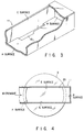
- the waveguide 11 has a surface (H surface) opposing the dielectric window 9 and perpendicular to the direction of electric field of the microwave, surfaces (E surfaces) extending perpendicularly to the H surface and parallel to the direction of electric field of the microwave, and a reflecting surface (short-circuiting surface; R surface) which is provided on a side opposite to the microwave introducing side perpendicularly to the H and E surfaces to reflect the microwave.
- Two slits 12 1 and 12 2 are formed in the H surface opposing the dielectric window 9 and located in the vicinity of the E surfaces, respectively, and extend along the E surfaces.
- the slits 12 1 and 12 2 have such a shape that their widths change stepwise to be smaller toward the reflecting surface (R surface).
- a wafer 13 having a resist pattern formed on its surface is set on the wafer holder 7 in the processing chamber 4 of the vacuum container 1.
- a vacuum pump (not shown) is actuated to exhaust gas in the vacuum container 1 through the exhaust pipe 8.
- a process gas e.g., oxygen gas
- a microwave is introduced from a microwave oscillator (not shown) into the waveguide 11, so that a plasma is generated in the plasma generating chamber 3 of the vacuum container 1.
- the generated plasma is introduced into the processing chamber 4 through the opening of the diffusion plate 2, and active oxygen atoms in the plasma react with the resist pattern on the surface of the wafer 13 set on the wafer holder 7 in the processing chamber 4 to remove the resist pattern. In other words, so-called ashing is performed.
- the two slits 12 1 and 12 2 are formed in the H surface of the waveguide 11 to have such a shape that their widths change stepwise to be smaller toward the reflecting surface (R surface). Therefore, a synthetic wave of an incident wave and a wave reflected by the reflecting surface (R surface) of the waveguide 11 are uniformed to make the radiation power of the microwave uniform. As a result, a uniform plasma can be generated in the plasma generating chamber 3 of the vacuum container 1 formed under the waveguide 11.
- the two slits 12 1 and 12 2 are formed in the H surface of the waveguide 11 opposing the dielectric window 9 and located in the vicinity of the E surfaces and extend along the E surfaces. More specifically, since the slits 12 1 and 12 2 are respectively formed in the H surface located in the vicinity of the E surfaces, where the field strength becomes almost zero, they can avoid the microwave incident on the waveguide 11 from being coupled to the electric field. For this reason, the microwave radiated from the slits 12 1 and 12 2 is not completely transmitted through the dielectric window 9 arranged in the opening portion 10 of the upper wall portion of the vacuum container 1 but can propagate along a dielectric line (e.g., a coplanar line or a slot line).
- a dielectric line e.g., a coplanar line or a slot line
- the microwave radiated from the slits 12 1 and 12 2 is reflected by a high-density plasma region in the plasma generating chamber 3, it can propagate through the dielectric window 9 and can be radiated to a low-density plasma region in the plasma generating chamber 3 again. Since the microwave can be absorbed by the plasma efficiently, a plasma which is stable in a wide pressure range can be generated.
- the present inventors confirmed through the following experiments that, with the microwave excitation plasma processing apparatus of the present invention, a plasma which is stable in a wider pressure range can be generated and that a more uniform plasma can be generated in the plasma generating chamber, when compared to a conventional microwave excitation plasma processing apparatus.
- a waveguide was used in which two slits 12 1 and 12 2 were formed in an H surface (width: 96 mm) opposing a dielectric window and located in the vicinity of an E surfaces, respectively, and extend along the E surfaces.
- Each of the slits 12 1 and 12 2 is of such a shape that changed stepwise and had a length of 170 mm, a narrow portion with a width of 11.5 mm on the reflecting surface (R surface) side, and a wide portion with a width of 15 mm.
- each of the two slits 12 1 and 12 2 is formed in the H surface such that its center in the longitudinal direction is located in the waveguide at a distance corresponding to the wavelength ( ⁇ g) of the microwave from the reflecting surface (R surface).
- a plasma generating chamber 3 of a vacuum container 1 had an inside diameter of 200 mm, and a dielectric window 9 had a diameter of 240 mm.
- a stable plasma whose reflected wave was 5 W or less could be generated under the conditions of an electric discharge region shown in Table 1.
- Table 1 Microwave Output 400 to 1000W Oxygen Supply Amount 1000sccm Pressure 5 to 200Pa
- the open hole 20 had a length of 200 mm, which corresponded to the inside diameter of a plasma generating chamber 3, and a width of 96 mm.
- a dielectric window 9 had a diameter of 240 mm, in the same manner as in Experimental Example 1 described above.
- the microwave excitation plasma processing apparatus of the present invention can generate a stable plasma in wide ranges of microwave outputs such as 400 to 1000W and pressures (5 to 200Pa) when compared to those of the conventional microwave excitation plasma processing apparatus.
- FIG. 5 is a photograph obtained by photographing a plasma generating state in the plasma generating chamber from the bottom portion side of the vacuum container of the microwave excitation plasma processing apparatus according to the present invention.
- FIG. 6 is a photograph obtained by photographing a plasma generating state in the plasma generating chamber from the bottom portion side of the vacuum container of the conventional microwave excitation plasma processing apparatus.
- the microwave excitation plasma processing apparatus of the present invention which shows the plasma generating state of FIG. 5 can generate a more uniform plasma in the plasma generating chamber than that of the conventional microwave excitation plasma processing apparatus which shows the plasma generating state of FIG. 6.
- the microwave excitation plasma processing apparatus can uniformly generate a plasma in a plasma generating chamber 3, it can efficiently ash a resist pattern on the surface of a wafer 13 set on a wafer holder 7 in a processing chamber 4.
- Embodiment 1 two slits having such a shape that changes stepwise so that their widths are reduced toward the reflecting surface (R surface) are formed in the H surface in the vicinity of the E surface to extend along the E surface.
- the present invention is not limited to this.
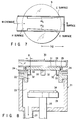
- a waveguide 11 as shown in FIG. 7 is used in which the two slits 14 1 and 14 2 , which are tapered so that their widths are reduced toward its reflecting surface (R surface) and are formed in the H surface opposing a dielectric window and located in the vicinity of E surfaces, respectively, and which extend along the E surfaces, in the introduction of a microwave into the waveguide.
- a stable plasma can be generated in wide ranges of microwave outputs and pressures, and a uniform plasma can be generated in the plasma generating chamber, in the same manner as in Embodiment 1 described above.
- the microwave excitation plasma processing apparatus is not limited to ashing for removing a resist pattern on a semiconductor wafer, but can similarly be applied to etching of a semiconductor wafer or various types of films on a semiconductor wafer or a glass substrate.
- CF 4 or SF 6 gas is used as a process gas which is supplied to the gas supply pipe.
- FIG. 8 is a schematic view showing a down flow type microwave excitation plasma processing apparatus applied to ashing of a resist on a wafer of Embodiment 2.
- a plasma generating chamber 22 and a processing chamber 23 are respectively formed in upper and lower portions of a vacuum container 21.
- Four gas supply pipes 24 are formed equiangularly (90x) in the side wall of the vacuum container 21 in which the plasma generating chamber 22 is formed.
- a wafer holder 26 having a rotating shaft 25 mounted on its lower surface is rotatably arranged in the processing chamber 23.
- An exhaust pipe 27 is mounted on the bottom portion of the vacuum container 21 where the processing chamber 23 is formed.
- An exhaust system (not shown), e.g., a vacuum pump, is connected with the other end of the exhaust pipe 27.
- a dielectric window 28 made of, e.g., quartz glass, is mounted in an opening portion 29 formed in the upper wall portion of the vacuum container 21.
- a rectangular waveguide 30 into which a microwave generated by a microwave oscillator (not shown) is introduced is arranged on the upper wall portion of the vacuum container 21 including the dielectric window 28.
- An elongated open hole 31 is formed in a surface (H surface) of the waveguide 30 perpendicular to the direction of electric field of the microwave to oppose the dielectric window 28.
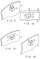
- Box-like shielding portions 32 each having an open upper portion are mounted on the inner surface of the vacuum container 21 to respectively surround output portions 33 of the gas supply pipes 24, as shown in FIGS. 9 and 10.
- a distance A between the center of the output portion 33 of each gas supply pipe 24 and the dielectric window 28 is preferably 2 to 20 mm.
- a distance B between the inner surface of the vacuum container 21 and the front surface of each box-like shielding portion 32 is preferably 1 to 10 mm.
- a distance C between the center of the output portion 33 of each gas supply pipe 24 and the bottom surface of the corresponding box-like shielding portion 32 is preferably 1 to 10 mm.
- a distance D between the center of the output portion 33 of each gas supply pipe 24 and the side surface of the corresponding box-like shielding portion 32 is preferably about 5 mm.
- a wafer 34 having a resist pattern formed on its surface is set on the wafer holder 26 in the processing chamber 23 of the vacuum container 21.
- a vacuum pump (not shown) is actuated to exhaust gas in the vacuum container 21 through the exhaust pipe 27.
- oxygen gas (reaction gas) is supplied to the plasma generating chamber 22 in the upper portion of the vacuum container 21 through the four gas supply pipes 24.
- the box-like shielding portions 32 each having an open upper portion are mounted on the inner surface of the vacuum container 21 in the vicinities of the output portions 33 of the gas supply pipes 24 to respectively surround the output portions 33.
- the oxygen gas blown from the output portions 33 of the gas supply pipes 24 is shielded by the shielding portions 32 and directed upward, as shown in FIGS.
- the oxygen gas is then supplied toward the center of the plasma generating chamber 22 along the lower surface of the dielectric window 28 arranged on the upper wall portion of the vacuum container 21.
- a microwave is introduced into the waveguide 30, so that a uniform plasma is generated in the plasma generating chamber 22 of the vacuum container 21.
- the generated plasma is introduced into the processing chamber 23, and active oxygen atoms in the plasma react with the resist pattern on the surface of the wafer 34 set on the wafer holder 26 in the processing chamber 23 to remove the resist pattern. In other words, so-called ashing is performed.
- the resist pattern on the surface of the wafer 34 can be uniformly ashed at a high rate without using a diffusion plate arranged between the plasma generating chamber 22 and the processing chamber 23, and contamination of the wafer with a metal or particles which is caused by ion radiation to the diffusion plate can be prevented.
- the present inventors confirmed through the following experiments that the microwave excitation plasma processing apparatus of Embodiment 2 could perform more uniform ashing at a higher rate than that in a microwave excitation plasma processing apparatus that blew gas in a different manner.
- Box-like shielding portions 32 each having an open upper portion, as shown in FIGS. 9 and 10, were mounted on the inner surface of a vacuum container 21 to respectively surround output portions 33 (diameter: 1 mm) of four gas supply pipes 24.
- a distance A between the center of the output portion 33 of each gas supply pipe 24 and a dielectric window 28 was set to 10 mm
- a distance B between the inner surface of the vacuum container 21 and the front surface of each box-like shielding portion 32 was set to 5 mm
- a distance C between the center of the output portion 33 of each gas supply pipe 24 and the bottom surface of the corresponding box-like shielding portion 32 was set to 5 mm
- a distance D between the center of the output portion 33 of each gas supply pipe 24 and the side surface of the corresponding box-like shielding portion 32 was set to 5 mm.
- a plasma generating chamber 22 of the vacuum container 21 had a diameter of 200 mm, the dielectric window 28 had a diameter of 240 mm, and the distance from the lower surface of the dielectric window 28 to the upper surface of a wafer holder 26 was set to 120 mm.
- a wafer having a surface entirely coated with a photoresist film was set on the wafer holder 26.
- This microwave excitation plasma processing apparatus generated a plasma in its plasma generating chamber under the following conditions in order to ash the resist film on the wafer set on the holder in the processing chamber.
- the ashing rate (solid circle) and ashing variations (hollow circle) of this ashing were calculated.
- FIG. 15 shows the result.
- a plasma was generated in a plasma generating chamber to ash a resist film on a wafer set on a holder in the processing chamber.
- the ashing rate (solid circle) and ashing variations (hollow circle) of this ashing were calculated.
- FIG. 15 shows the result.
- the oxygen gas was supplied as indicated by arrows A in FIG. 12.
- Box-like shielding portions 35 each having open right and left side surfaces were mounted on the inner surface of a vacuum container 21 to respectively surround output portions 33 (diameter: 1 mm) of four gas supply pipes, as shown in FIG. 13.
- the positional relationship between the output portions 33 of the gas supply pipes and the box-like shielding portions 35, the shape of the vacuum container, and the like were the same as those of Experimental Example 4.
- This microwave excitation plasma processing apparatus generated a plasma in its plasma generating chamber under the following conditions in order to ash a resist film on a wafer set on a holder in the processing chamber.
- the ashing rate (solid circle) and ashing variations (hollow circle) of this ashing were calculated.
- FIG. 15 shows the result.
- the oxygen gas was supplied as indicated by arrows B in FIG. 12.
- Box-like shielding portions 36 each having an open upper wall and an open bottom portion were mounted on the inner surface of a vacuum container 21 to respectively surround output portions 33 (diameter: 1 mm) of four gas supply pipes, as shown in FIG. 13.
- the positional relationship between the output portions 33 of the gas supply pipes and the box-like shielding portions 36, the shape of the vacuum container, and the like were the same as those of Experimental Example 4.
- This microwave excitation plasma processing apparatus generated a plasma in its plasma generating chamber under the following conditions in order to ash a resist film on a wafer set on a holder in the processing chamber.
- the ashing rate (solid circle) and ashing variations (hollow circle) of this ashing were calculated.
- FIG. 15 shows the result.
- the oxygen gas was supplied as indicated by arrows C in FIG. 12.
- Embodiment 2 described above four gas supply pipes are mounted on a portion of the side wail of the vacuum container which corresponds to the plasma generating chamber.
- the present invention is not limited to this, and two or three gas supply pipes, or five or more gas supply pipes can be mounted.
- the microwave excitation plasma processing apparatus can generate a stable plasma in the wide ranges of microwave outputs and pressures in the plasma generating chamber, and can generate a uniform plasma in the plasma generating chamber. Therefore, with the microwave excitation plasma processing apparatus according to the present invention, ashing of a resist pattern after pattern formation on a semiconductor substrate or a glass substrate, and etching of a semiconductor substrate or various types of films by using a resist pattern as a mask can be performed efficiently.
Abstract
Description
- The present invention relates to a microwave excitation plasma processing apparatus used for etching and ashing in the manufacture of a semiconductor device and the like.
- As a conventional microwave excitation plasma processing apparatus, one having a structure disclosed in Jpn. Pat. Appln. KOKAI Publication No. 61-131454 is known. This plasma processing apparatus has a vacuum container, a dielectric window, a waveguide, and a microwave oscillator. The vacuum container has a plasma generating chamber at its upper portion and a processing chamber which is formed under the plasma generating chamber and in which a processing target member is arranged. The dielectric window is arranged in the opening of the upper wall portion of the vacuum container. The waveguide is arranged on the upper wall portion of the vacuum container including the dielectric window. The microwave oscillator introduces a microwave into the waveguide. The waveguide has a rectangular shape. A surface (H surface) of the waveguide which is perpendicular to the direction of electric field of the microwave opposes the dielectric window. Surfaces (E surfaces) of the waveguide which is parallel to the direction of electric field of the microwave extends in a direction perpendicular to the H surface, respectively. The waveguide also has a reflecting surface which is provided on a side opposite to the microwave introducing side perpendicularly to the H and E surfaces to reflect the microwave. The opening portion is formed in an entire H surface portion of the waveguide that opposes the dielectric window. The microwave is introduced from the opening portion into the plasma generating chamber through the dielectric window.
- In the microwave excitation plasma processing apparatus described above, the field strength of the microwave introduced into the plasma generating chamber is determined by the synthetic wave of an incident wave which propagates from the microwave oscillator through the waveguide located in the upper portion of the plasma generating chamber and a wave reflected by the reflecting surface (short-circuiting wave) of the waveguide. The incident wave is introduced into the plasma generating chamber through the dielectric window and propagates as it is attenuated by being absorbed by the plasma generated in the generating chamber. The microwave which has propagated to the short-circuiting surface of the waveguide is reflected by the short-circuiting surface, is introduced into the plasma generating chamber through the dielectric window, and propagates as it is attenuated by being absorbed by the plasma in the same manner as the incident wave. At this time, the distribution of electric field of the synthetic wave is strong on the short-circuiting surface side of the waveguide and is weak on the input side of the waveguide. Therefore, the distribution of electric field in the plasma generating chamber varies to make the plasma nonuniform. As a result, etching and ashing by the plasma processing apparatus become nonuniform.
- The electric field of the microwave propagating in the waveguide is distributed sinusoidally with reference to the E surface as the node. When the microwave is of the TE01 mode, the electric field is largest at the center of the waveguide and is small near the E surface. In the conventional microwave excitation plasma processing apparatus described above, since the largest electric field of the microwave propagating in the waveguide is passed through the dielectric window serving also as a vacuum seal to be coupled with the plasma (load) directly, the microwave is absorbed by the plasma mainly at a portion (the center of the waveguide) where the field strength of the microwave is high. Therefore, the plasma has such a distribution that its density is high at the portion (the center of the waveguide) where the field strength is high and is lower toward a portion (on the E surface side of the waveguide) where the field strength is low. When the central density of the plasma reaches a value to shield the microwave, the microwave is not transmitted to the plasma generating chamber. At this time, the microwave is not absorbed depending on the state of the plasma, and the reflected wave becomes so large that its average reflectance of one-minute electric discharge sometimes exceeds about 50%. Therefore, an efficiency of ionizing the gas introduced into the plasma generating chamber is decreased to decrease the etching or ashing rate.
- It is an object of the present invention to provide a microwave excitation plasma processing apparatus which can generate a stable plasma in wide ranges of microwave outputs and pressures in the plasma generating chamber of a vacuum container, and which can efficiently etch or ash a processing target member in the processing chamber located under the generating chamber by generating a uniform plasma in the plasma generating chamber.
- According to the present invention, there is provided a microwave excitation plasma processing apparatus comprising:
- a vacuum container having a plasma generating chamber at an upper portion thereof and a processing chamber which is formed under the plasma generating chamber and in which a processing target member is arranged;
- a gas supply means for supplying a process gas into the plasma generating chamber;
- a dielectric window arranged in an opening of an upper wall portion of the vacuum container;
- a rectangular waveguide arranged on the upper wall portion of the vacuum container including the dielectric window and having a surface (H surface) perpendicular to a direction of electric field of a microwave to oppose the dielectric window, surfaces (E surfaces) parallel to the direction of electric field of the microwave and extending in a direction perpendicular to the H surface, and a reflecting surface which is provided on a side opposite to a microwave introducing side perpendicularly to the H and E surfaces to reflect the microwave; and
- a microwave oscillator for introducing the microwave into the waveguide,
- In the microwave excitation plasma processing apparatus according to the present invention, the slits formed in the waveguide preferably have a shape as follows:
- (1) Each slit has such a shape that its width changes stepwise to be smaller toward the reflecting surface.
- (2) Each slit has such a shape that its width changes in a tapered manner to be smaller toward the reflecting surface.
- It is preferable that the length (L) of each slit is defined as


- In the microwave excitation plasma processing apparatus according to the present invention, a rectangular waveguide arranged on the upper wall portion of the vacuum container including the dielectric window and having a surface (H surface) perpendicular to a direction of electric field of a microwave to oppose the dielectric window, surfaces (E surfaces) parallel to the direction of electric field of the microwave and extending in a direction perpendicular to the H surface, and a reflecting surface which is provided on a side opposite to a microwave introducing side perpendicularly to the H and E surfaces to reflect the microwave. The waveguide has two slits which are formed in the H surface opposing the dielectric window and located in the vicinity of the E surfaces, respectively, and which extend in parallel or substantially parallel to the E surfaces. Each of the slits having a width which is smaller on a side closer to the reflecting surface. When a microwave is introduced from the microwave oscillator into the waveguide, since two slits are open in the H surface of the waveguide and being narrower on a side closer to the reflecting surface of the waveguide, a synthetic wave of an incident wave and a wave reflected by the reflecting surface (short-circuiting surface) of the waveguide can be uniformed, thereby making the radiation power of the microwave uniform. As a result, the microwave having a uniform radiation output can be radiated from the waveguide into the plasma generating chamber in the vacuum container through the dielectric window arranged under the waveguide, thereby generating a uniform plasma in the generating chamber.
- The two slits are respectively open in a portion of the H surface opposing the dielectric window and located in the vicinity of the E surfaces, where the field strength becomes almost zero. Therefore, the microwave incident on the waveguide can be prevented from being coupled to the electric field. Hence, the microwave radiated from the slits is not completely transmitted through the dielectric window arranged in the opening of the upper wall portion of the vacuum container but can propagate along a dielectric line (e.g., a coplanar line or a slot line). As a result, even if the microwave radiated from the slits is reflected by a high-density plasma region in the plasma generating chamber, it can propagate through the dielectric window and can be radiated to a low-density plasma region in the plasma generating chamber again. This increases an absorption efficiency at which the microwave is absorbed by the plasma. Therefore, a stable plasma can be generated in a wide pressure range.
- A stable plasma can be generated in the wide ranges of microwave outputs and pressures in the plasma generating chamber of the vacuum container, and a uniform plasma can be generated in the plasma generating chamber, so that a processing target member arranged in the processing chamber under the plasma generating chamber of the vacuum container can be etched or ashed efficiently.
- This invention can be more fully understood from the following detailed description when taken in conjunction with the accompanying drawings, in which:
- FIG. 1 is a schematic view showing a microwave excitation plasma processing apparatus according to Embodiment 1 of the present invention;
- FIG. 2 is a cross-sectional view of the main part of FIG. 1;
- FIG. 3 is a partially cutaway perspective view showing a waveguide of FIG. 1;
- FIG. 4 is a cross-sectional view of a waveguide used in a conventional microwave excitation plasma processing apparatus;
- FIG. 5 is a photograph obtained by photographing a plasma generating state in a plasma generating chamber from the bottom portion side of the vacuum container of a microwave excitation plasma processing apparatus according to the present invention;
- FIG. 6 is a photograph obtained by photographing a plasma generating state in the plasma generating chamber from the bottom portion side of the vacuum container of the conventional microwave excitation plasma processing apparatus;
- FIG. 7 is a cross-sectional view of a waveguide used in a microwave excitation plasma processing apparatus according to a modification of Embodiment 1 of the present invention;
- FIG. 8 is a schematic diagram showing a microwave excitation plasma processing apparatus according to
Embodiment 2; - FIG. 9 is a partially enlarged perspective view showing the structure of a portion near the output portion of a gas supply pipe of FIG. 8;
- FIG. 10 is a sectional view of the main part of FIG. 8;
- FIG. 11 is a perspective view showing the flow of oxygen gas in the microwave excitation plasma processing apparatus of FIG. 8;
- FIG. 12 is a perspective view showing the flow of oxygen gas in the microwave excitation plasma processing apparatuses of Experimental Examples 5 to 7;
- FIG. 13 is a partially enlarged perspective view showing the structure of a portion near the output portion of a gas supply pipe of Experimental Example 6;
- FIG. 14 is a partially enlarged perspective view showing the structure of a portion near the output portion of a gas supply pipe of Experimental Example 7; and
- FIG. 15 is a graph showing an ashing rate and ashing variations of the microwave excitation plasma processing apparatuses of Experimental Examples 4 to 7.
- The preferred embodiments of the present invention will be described in detail with reference to the accompanying drawings.
- FIG. 1 is a schematic view showing a down flow type microwave excitation plasma processing apparatus applied to ashing of a resist on a wafer of Embodiment 1.
- The interior of a vacuum container 1 is vertically divided into a
plasma generating chamber 3 and aprocessing chamber 4 with a horizontally arrangeddiffusion plate 2 made of, e.g., a mesh-like metal member. Agas supply pipe 5 is formed in the side wall of theplasma generating chamber 3 in the upper portion of the vacuum container 1. Awafer holder 7 having arotating shaft 6 mounted on its lower surface is rotatably arranged in theprocessing chamber 4. An exhaust pipe 8 is mounted on the bottom portion of the vacuum container 1 where theprocessing chamber 4 is formed. An exhaust system (not shown), e.g., a vacuum pump, is connected with the other end of the exhaust pipe 8. - A
dielectric window 9 made of quartz glass is mounted in anopening portion 10 formed in the upper wall portion of the vacuum container 1. Thedielectric window 9 may be made of alumina instead. A microwave generated by a microwave oscillator (not shown) is introduced into arectangular waveguide 11. Thewaveguide 11 is arranged on the upper wall portion of the vacuum container 1 including thedielectric window 9. As shown in FIGS. 2 and 3, thewaveguide 11 has a surface (H surface) opposing thedielectric window 9 and perpendicular to the direction of electric field of the microwave, surfaces (E surfaces) extending perpendicularly to the H surface and parallel to the direction of electric field of the microwave, and a reflecting surface (short-circuiting surface; R surface) which is provided on a side opposite to the microwave introducing side perpendicularly to the H and E surfaces to reflect the microwave. Two slits 121 and 122 are formed in the H surface opposing thedielectric window 9 and located in the vicinity of the E surfaces, respectively, and extend along the E surfaces. The slits 121 and 122 have such a shape that their widths change stepwise to be smaller toward the reflecting surface (R surface). - A method of ashing a wafer having a resist pattern formed on its surface with the microwave excitation plasma processing apparatus described above will be described.
- A
wafer 13 having a resist pattern formed on its surface is set on thewafer holder 7 in theprocessing chamber 4 of the vacuum container 1. A vacuum pump (not shown) is actuated to exhaust gas in the vacuum container 1 through the exhaust pipe 8. Simultaneously, a process gas, e.g., oxygen gas, is supplied to theplasma generating chamber 3 in the upper portion of the vacuum container 1 through thegas supply pipe 5. When the interior of the vacuum container 1 reaches a predetermined pressure, a microwave is introduced from a microwave oscillator (not shown) into thewaveguide 11, so that a plasma is generated in theplasma generating chamber 3 of the vacuum container 1. The generated plasma is introduced into theprocessing chamber 4 through the opening of thediffusion plate 2, and active oxygen atoms in the plasma react with the resist pattern on the surface of thewafer 13 set on thewafer holder 7 in theprocessing chamber 4 to remove the resist pattern. In other words, so-called ashing is performed. - In introduction of the microwave into the
waveguide 11, as shown in FIGS. 2 and 3, the two slits 121 and 122 are formed in the H surface of thewaveguide 11 to have such a shape that their widths change stepwise to be smaller toward the reflecting surface (R surface). Therefore, a synthetic wave of an incident wave and a wave reflected by the reflecting surface (R surface) of thewaveguide 11 are uniformed to make the radiation power of the microwave uniform. As a result, a uniform plasma can be generated in theplasma generating chamber 3 of the vacuum container 1 formed under thewaveguide 11. - The two slits 121 and 122 are formed in the H surface of the
waveguide 11 opposing thedielectric window 9 and located in the vicinity of the E surfaces and extend along the E surfaces. More specifically, since the slits 121 and 122 are respectively formed in the H surface located in the vicinity of the E surfaces, where the field strength becomes almost zero, they can avoid the microwave incident on thewaveguide 11 from being coupled to the electric field. For this reason, the microwave radiated from the slits 121 and 122 is not completely transmitted through thedielectric window 9 arranged in the openingportion 10 of the upper wall portion of the vacuum container 1 but can propagate along a dielectric line (e.g., a coplanar line or a slot line). As a result, even if the microwave radiated from the slits 121 and 122 is reflected by a high-density plasma region in theplasma generating chamber 3, it can propagate through thedielectric window 9 and can be radiated to a low-density plasma region in theplasma generating chamber 3 again. Since the microwave can be absorbed by the plasma efficiently, a plasma which is stable in a wide pressure range can be generated. - In fact, the present inventors confirmed through the following experiments that, with the microwave excitation plasma processing apparatus of the present invention, a plasma which is stable in a wider pressure range can be generated and that a more uniform plasma can be generated in the plasma generating chamber, when compared to a conventional microwave excitation plasma processing apparatus.
- A waveguide was used in which two slits 121 and 122 were formed in an H surface (width: 96 mm) opposing a dielectric window and located in the vicinity of an E surfaces, respectively, and extend along the E surfaces. Each of the slits 121 and 122 is of such a shape that changed stepwise and had a length of 170 mm, a narrow portion with a width of 11.5 mm on the reflecting surface (R surface) side, and a wide portion with a width of 15 mm. Note that each of the two slits 121 and 122 is formed in the H surface such that its center in the longitudinal direction is located in the waveguide at a distance corresponding to the wavelength (λg) of the microwave from the reflecting surface (R surface). A
plasma generating chamber 3 of a vacuum container 1 had an inside diameter of 200 mm, and adielectric window 9 had a diameter of 240 mm. - In this microwave excitation plasma processing apparatus according to the present invention, a stable plasma whose reflected wave was 5 W or less could be generated under the conditions of an electric discharge region shown in Table 1.
Table 1 Microwave Output 400 to 1000W Oxygen Supply Amount 1000sccm Pressure 5 to 200Pa - A waveguide having an elongated
open hole 20 formed in its H surface, as shown in FIG. 4, was used. Theopen hole 20 had a length of 200 mm, which corresponded to the inside diameter of aplasma generating chamber 3, and a width of 96 mm. Adielectric window 9 had a diameter of 240 mm, in the same manner as in Experimental Example 1 described above. - In this (conventional) microwave excitation plasma processing apparatus according to Experimental Example 2, a stable plasma whose reflected wave was 5 W or less could be generated under the conditions of an electric discharge region shown in Table 2.
Table 2 Microwave Output 700 to 1000W Oxygen Supply Amount 1000sccm Pressure 70 to 200Pa - From the results of Tables 1 and 2, it can be known that the microwave excitation plasma processing apparatus of the present invention can generate a stable plasma in wide ranges of microwave outputs such as 400 to 1000W and pressures (5 to 200Pa) when compared to those of the conventional microwave excitation plasma processing apparatus.
- A microwave excitation plasma processing apparatus according to the present invention and a conventional microwave excitation plasma processing apparatus were employed. The former used a waveguide in which two slits 121 and 122 of such a shape that changed stepwise, as shown in FIGS. 2 and 3, and of the same size as that of Experimental Example 1 were formed in an H surface (width: 96 mm) opposing a dielectric window and located in the vicinity of an E surfaces, respectively, and extend along the E surfaces. The latter used a waveguide in which an elongated
open hole 20 as shown in FIG. 4, which had the same size as that of Experimental Example 2 was formed in its H surface. A plasma was generated under the conditions shown in Table 3.Table 3 Microwave Output 1kW Oxygen Supply Amount 200sccm Pressure 70Pa - FIG. 5 is a photograph obtained by photographing a plasma generating state in the plasma generating chamber from the bottom portion side of the vacuum container of the microwave excitation plasma processing apparatus according to the present invention. FIG. 6 is a photograph obtained by photographing a plasma generating state in the plasma generating chamber from the bottom portion side of the vacuum container of the conventional microwave excitation plasma processing apparatus.
- It can be known that the microwave excitation plasma processing apparatus of the present invention which shows the plasma generating state of FIG. 5 can generate a more uniform plasma in the plasma generating chamber than that of the conventional microwave excitation plasma processing apparatus which shows the plasma generating state of FIG. 6.
- Since the microwave excitation plasma processing apparatus according to the present invention can uniformly generate a plasma in a
plasma generating chamber 3, it can efficiently ash a resist pattern on the surface of awafer 13 set on awafer holder 7 in aprocessing chamber 4. - In Embodiment 1, two slits having such a shape that changes stepwise so that their widths are reduced toward the reflecting surface (R surface) are formed in the H surface in the vicinity of the E surface to extend along the E surface. However, the present invention is not limited to this. A
waveguide 11 as shown in FIG. 7 is used in which the two slits 141 and 142, which are tapered so that their widths are reduced toward its reflecting surface (R surface) and are formed in the H surface opposing a dielectric window and located in the vicinity of E surfaces, respectively, and which extend along the E surfaces, in the introduction of a microwave into the waveguide. Nonetheless, a stable plasma can be generated in wide ranges of microwave outputs and pressures, and a uniform plasma can be generated in the plasma generating chamber, in the same manner as in Embodiment 1 described above. - The microwave excitation plasma processing apparatus according to the present invention is not limited to ashing for removing a resist pattern on a semiconductor wafer, but can similarly be applied to etching of a semiconductor wafer or various types of films on a semiconductor wafer or a glass substrate. For example, when the microwave excitation plasma processing apparatus according to the present invention is applied to etching of a polysilicon film on a semiconductor substrate, CF4 or SF6 gas is used as a process gas which is supplied to the gas supply pipe.
- FIG. 8 is a schematic view showing a down flow type microwave excitation plasma processing apparatus applied to ashing of a resist on a wafer of
Embodiment 2. - A
plasma generating chamber 22 and aprocessing chamber 23 are respectively formed in upper and lower portions of avacuum container 21. Fourgas supply pipes 24 are formed equiangularly (90x) in the side wall of thevacuum container 21 in which theplasma generating chamber 22 is formed. Awafer holder 26 having a rotatingshaft 25 mounted on its lower surface is rotatably arranged in theprocessing chamber 23. Anexhaust pipe 27 is mounted on the bottom portion of thevacuum container 21 where theprocessing chamber 23 is formed. An exhaust system (not shown), e.g., a vacuum pump, is connected with the other end of theexhaust pipe 27. Adielectric window 28 made of, e.g., quartz glass, is mounted in anopening portion 29 formed in the upper wall portion of thevacuum container 21. Arectangular waveguide 30 into which a microwave generated by a microwave oscillator (not shown) is introduced is arranged on the upper wall portion of thevacuum container 21 including thedielectric window 28. An elongatedopen hole 31 is formed in a surface (H surface) of thewaveguide 30 perpendicular to the direction of electric field of the microwave to oppose thedielectric window 28. - Box-
like shielding portions 32 each having an open upper portion are mounted on the inner surface of thevacuum container 21 to respectively surroundoutput portions 33 of thegas supply pipes 24, as shown in FIGS. 9 and 10. A distance A between the center of theoutput portion 33 of eachgas supply pipe 24 and thedielectric window 28 is preferably 2 to 20 mm. A distance B between the inner surface of thevacuum container 21 and the front surface of each box-like shielding portion 32 is preferably 1 to 10 mm. A distance C between the center of theoutput portion 33 of eachgas supply pipe 24 and the bottom surface of the corresponding box-like shielding portion 32 is preferably 1 to 10 mm. A distance D between the center of theoutput portion 33 of eachgas supply pipe 24 and the side surface of the corresponding box-like shielding portion 32 is preferably about 5 mm. - A method of ashing a wafer having a resist pattern formed on its surface with the microwave excitation plasma processing apparatus described above will be described.
- A
wafer 34 having a resist pattern formed on its surface is set on thewafer holder 26 in theprocessing chamber 23 of thevacuum container 21. A vacuum pump (not shown) is actuated to exhaust gas in thevacuum container 21 through theexhaust pipe 27. Simultaneously, oxygen gas (reaction gas) is supplied to theplasma generating chamber 22 in the upper portion of thevacuum container 21 through the fourgas supply pipes 24. At this time, the box-like shielding portions 32 each having an open upper portion are mounted on the inner surface of thevacuum container 21 in the vicinities of theoutput portions 33 of thegas supply pipes 24 to respectively surround theoutput portions 33. Thus, the oxygen gas blown from theoutput portions 33 of thegas supply pipes 24 is shielded by the shieldingportions 32 and directed upward, as shown in FIGS. 9 and 11. The oxygen gas is then supplied toward the center of theplasma generating chamber 22 along the lower surface of thedielectric window 28 arranged on the upper wall portion of thevacuum container 21. In this oxygen gas supply, when the interior of thevacuum container 21 reaches a predetermined pressure, a microwave is introduced into thewaveguide 30, so that a uniform plasma is generated in theplasma generating chamber 22 of thevacuum container 21. The generated plasma is introduced into theprocessing chamber 23, and active oxygen atoms in the plasma react with the resist pattern on the surface of thewafer 34 set on thewafer holder 26 in theprocessing chamber 23 to remove the resist pattern. In other words, so-called ashing is performed. - Therefore, according to the microwave excitation plasma processing apparatus of
Embodiment 2, the resist pattern on the surface of thewafer 34 can be uniformly ashed at a high rate without using a diffusion plate arranged between theplasma generating chamber 22 and theprocessing chamber 23, and contamination of the wafer with a metal or particles which is caused by ion radiation to the diffusion plate can be prevented. - In fact, the present inventors confirmed through the following experiments that the microwave excitation plasma processing apparatus of
Embodiment 2 could perform more uniform ashing at a higher rate than that in a microwave excitation plasma processing apparatus that blew gas in a different manner. - Box-
like shielding portions 32 each having an open upper portion, as shown in FIGS. 9 and 10, were mounted on the inner surface of avacuum container 21 to respectively surround output portions 33 (diameter: 1 mm) of fourgas supply pipes 24. A distance A between the center of theoutput portion 33 of eachgas supply pipe 24 and adielectric window 28 was set to 10 mm, a distance B between the inner surface of thevacuum container 21 and the front surface of each box-like shielding portion 32 was set to 5 mm, a distance C between the center of theoutput portion 33 of eachgas supply pipe 24 and the bottom surface of the corresponding box-like shielding portion 32 was set to 5 mm, and a distance D between the center of theoutput portion 33 of eachgas supply pipe 24 and the side surface of the corresponding box-like shielding portion 32 was set to 5 mm. Aplasma generating chamber 22 of thevacuum container 21 had a diameter of 200 mm, thedielectric window 28 had a diameter of 240 mm, and the distance from the lower surface of thedielectric window 28 to the upper surface of awafer holder 26 was set to 120 mm. A wafer having a surface entirely coated with a photoresist film was set on thewafer holder 26. - This microwave excitation plasma processing apparatus generated a plasma in its plasma generating chamber under the following conditions in order to ash the resist film on the wafer set on the holder in the processing chamber. The ashing rate (solid circle) and ashing variations (hollow circle) of this ashing were calculated. FIG. 15 shows the result. The ashing variations (e) were calculated from the maximum ashing amount (max) and the minimum ashing amount (min) in accordance with the following equation:

〈Conditions for Generating Plasma〉 microwave output: 1 kW oxygen supply amount of each supply pipe: 50 sccm pressure: 70 Pa - Under the same conditions as in Experimental Example 4 except for not providing a shielding portion, a plasma was generated in a plasma generating chamber to ash a resist film on a wafer set on a holder in the processing chamber. The ashing rate (solid circle) and ashing variations (hollow circle) of this ashing were calculated. FIG. 15 shows the result. In Experimental Example 5, the oxygen gas was supplied as indicated by arrows A in FIG. 12.
- Box-
like shielding portions 35 each having open right and left side surfaces were mounted on the inner surface of avacuum container 21 to respectively surround output portions 33 (diameter: 1 mm) of four gas supply pipes, as shown in FIG. 13. The positional relationship between theoutput portions 33 of the gas supply pipes and the box-like shielding portions 35, the shape of the vacuum container, and the like were the same as those of Experimental Example 4. This microwave excitation plasma processing apparatus generated a plasma in its plasma generating chamber under the following conditions in order to ash a resist film on a wafer set on a holder in the processing chamber. The ashing rate (solid circle) and ashing variations (hollow circle) of this ashing were calculated. FIG. 15 shows the result. In Experimental Example 6, the oxygen gas was supplied as indicated by arrows B in FIG. 12. - Box-
like shielding portions 36 each having an open upper wall and an open bottom portion were mounted on the inner surface of avacuum container 21 to respectively surround output portions 33 (diameter: 1 mm) of four gas supply pipes, as shown in FIG. 13. The positional relationship between theoutput portions 33 of the gas supply pipes and the box-like shielding portions 36, the shape of the vacuum container, and the like were the same as those of Experimental Example 4. This microwave excitation plasma processing apparatus generated a plasma in its plasma generating chamber under the following conditions in order to ash a resist film on a wafer set on a holder in the processing chamber. The ashing rate (solid circle) and ashing variations (hollow circle) of this ashing were calculated. FIG. 15 shows the result. In Experimental Example 7, the oxygen gas was supplied as indicated by arrows C in FIG. 12. - As is apparent from FIG. 15, it can be known that the microwave excitation plasma processing apparatus of Experimental Example 4 which corresponds to
Embodiment 2 can perform ashing at a higher rate and more uniformly when compared to the microwave excitation plasma processing apparatuses of Experimental Examples 5 to 7. - In the microwave excitation plasma processing apparatus according to
Embodiment 2, when the distance between the lower surface of thedielectric window 9 and the upper surface of thewafer holder 7 is set to 120 mm or more, ions in the plasma are recombined before they reach the wafer. Thus, damage to the wafer caused by ion bombardment can be prevented. - In
Embodiment 2 described above, four gas supply pipes are mounted on a portion of the side wail of the vacuum container which corresponds to the plasma generating chamber. However, the present invention is not limited to this, and two or three gas supply pipes, or five or more gas supply pipes can be mounted. - As has been described above in detail, the microwave excitation plasma processing apparatus according to the present invention can generate a stable plasma in the wide ranges of microwave outputs and pressures in the plasma generating chamber, and can generate a uniform plasma in the plasma generating chamber. Therefore, with the microwave excitation plasma processing apparatus according to the present invention, ashing of a resist pattern after pattern formation on a semiconductor substrate or a glass substrate, and etching of a semiconductor substrate or various types of films by using a resist pattern as a mask can be performed efficiently.
Claims (9)
- A microwave excitation plasma processing apparatus characterized by comprising:a vacuum container (1) having a plasma generating chamber (3) at an upper portion thereof and a processing chamber (4) which is formed under the plasma generating chamber (3) and in which a processing target member (13) is arranged;a gas supply means (5) for supplying a process gas into the plasma generating chamber (3);a dielectric window (9) arranged in an opening (10) of an upper wall portion of the vacuum container (1);a rectangular waveguide (11) arranged on the upper wall portion of the vacuum container (1) including the dielectric window (9) and having a surface (H surface) perpendicular to a direction of electric field of a microwave to oppose the dielectric window (9), surfaces (E surfaces) parallel to the direction of electric field of the microwave and extending in a direction perpendicular to the H surface, and a reflecting surface which is provided on a side opposite to a microwave introducing side perpendicularly to the H and E surfaces to reflect the microwave; anda microwave oscillator for introducing the microwave into the waveguide (11),wherein the waveguide (11) has two slits (121, 122) which are formed in the H surface opposing the dielectric window (9) and located in the vicinity of the E surfaces, respectively, and which extend parallel or substantially parallel to the E surfaces, each of the slits (121, 122) having a width which is smaller on a side closer to the reflecting surface.
- The apparatus according to claim 1, characterized in that the vacuum container (1) is divided into the plasma generating chamber (3) and the processing chamber (4) by a diffusion plate (2) arranged horizontally.
- The apparatus according to claim 1, characterized in that the process gas consists of one of oxygen gas and a gas mixture containing oxygen gas and an inert gas.
- The apparatus according to claim 1, characterized in that the process gas consists of one of CF4 gas and SF6 gas.
- The apparatus according to claim 1, characterized in that the dielectric window (9) is made of quartz glass.
- The apparatus according to claim 1, characterized in that each of the slits (121, 122) has such a shape that a width thereof changes stepwise to be smaller toward the reflecting surface of the waveguide (11).
- The apparatus according to claim 1, characterized in that each of the slits (141, 142) has such a shape that a width thereof changes in a tapered manner to be smaller toward the reflecting surface of the waveguide (11).
- The apparatus according to claim 1, characterized in that a length (L) of each of the slits (121, 122) is defined as

- The apparatus according to claim 1, characterized in that each of the slits (121, 122) has a central position in a longitudinal direction which is remote from the reflecting surface as a reference by a distance corresponding to a wavelength (λ/g) of the microwave introduced into the waveguide (11).
Applications Claiming Priority (6)
| Application Number | Priority Date | Filing Date | Title |
|---|---|---|---|
| JP7303363A JP2857090B2 (en) | 1995-10-30 | 1995-10-30 | Microwave-excited plasma processing equipment |
| JP303363/95 | 1995-10-30 | ||
| JP30336395 | 1995-10-30 | ||
| JP7281685A JP2791298B2 (en) | 1995-10-30 | 1995-10-30 | Microwave-excited plasma processing equipment |
| JP281685/95 | 1995-10-30 | ||
| JP28168595 | 1995-10-30 |
Publications (2)
| Publication Number | Publication Date |
|---|---|
| EP0777257A1 true EP0777257A1 (en) | 1997-06-04 |
| EP0777257B1 EP0777257B1 (en) | 1999-08-25 |
Family
ID=26554283
Family Applications (1)
| Application Number | Title | Priority Date | Filing Date |
|---|---|---|---|
| EP96110433A Expired - Lifetime EP0777257B1 (en) | 1995-10-30 | 1996-06-27 | Microwave excitation plasma processing apparatus |
Country Status (3)
| Country | Link |
|---|---|
| EP (1) | EP0777257B1 (en) |
| KR (1) | KR100234813B1 (en) |
| DE (1) | DE69603930T2 (en) |
Cited By (2)
| Publication number | Priority date | Publication date | Assignee | Title |
|---|---|---|---|---|
| EP1895565A1 (en) * | 2006-09-01 | 2008-03-05 | Canon Kabushiki Kaisha | Plasma processing apparatus and method |
| CN113038683A (en) * | 2021-03-09 | 2021-06-25 | 珠海恒格微电子装备有限公司 | Microwave plasma generating device and plasma etching equipment |
Families Citing this family (1)
| Publication number | Priority date | Publication date | Assignee | Title |
|---|---|---|---|---|
| JP4304053B2 (en) * | 2003-11-17 | 2009-07-29 | 株式会社アルバック | Microwave excitation plasma processing equipment |
Citations (3)
| Publication number | Priority date | Publication date | Assignee | Title |
|---|---|---|---|---|
| EP0480273A1 (en) * | 1990-10-06 | 1992-04-15 | Röhm Gmbh | Microwave Radiator |
| EP0564082A1 (en) * | 1992-03-30 | 1993-10-06 | Daihen Corporation | Plasma processing apparatus for generating uniform strip-shaped plasma |
| DE4431785A1 (en) * | 1994-04-11 | 1995-10-12 | Wu Jeng Ming | Plasma device |
-
1996
- 1996-06-27 DE DE69603930T patent/DE69603930T2/en not_active Expired - Lifetime
- 1996-06-27 EP EP96110433A patent/EP0777257B1/en not_active Expired - Lifetime
- 1996-10-11 KR KR1019960045179A patent/KR100234813B1/en not_active IP Right Cessation
Patent Citations (3)
| Publication number | Priority date | Publication date | Assignee | Title |
|---|---|---|---|---|
| EP0480273A1 (en) * | 1990-10-06 | 1992-04-15 | Röhm Gmbh | Microwave Radiator |
| EP0564082A1 (en) * | 1992-03-30 | 1993-10-06 | Daihen Corporation | Plasma processing apparatus for generating uniform strip-shaped plasma |
| DE4431785A1 (en) * | 1994-04-11 | 1995-10-12 | Wu Jeng Ming | Plasma device |
Cited By (3)
| Publication number | Priority date | Publication date | Assignee | Title |
|---|---|---|---|---|
| EP1895565A1 (en) * | 2006-09-01 | 2008-03-05 | Canon Kabushiki Kaisha | Plasma processing apparatus and method |
| CN113038683A (en) * | 2021-03-09 | 2021-06-25 | 珠海恒格微电子装备有限公司 | Microwave plasma generating device and plasma etching equipment |
| CN113038683B (en) * | 2021-03-09 | 2023-07-25 | 珠海恒格微电子装备有限公司 | Microwave plasma generating device and plasma etching equipment |
Also Published As
| Publication number | Publication date |
|---|---|
| KR100234813B1 (en) | 1999-12-15 |
| DE69603930T2 (en) | 2000-02-17 |
| DE69603930D1 (en) | 1999-09-30 |
| KR970023771A (en) | 1997-05-30 |
| EP0777257B1 (en) | 1999-08-25 |
Similar Documents
| Publication | Publication Date | Title |
|---|---|---|
| US4512868A (en) | Microwave plasma processing apparatus | |
| US4987284A (en) | Downstream microwave plasma processing apparatus having an improved coupling structure between microwave plasma | |
| US4970435A (en) | Plasma processing apparatus | |
| EP1177112B1 (en) | Remote plasma generator | |
| JP3288490B2 (en) | Semiconductor device manufacturing method and semiconductor device manufacturing apparatus | |
| US5364519A (en) | Microwave plasma processing process and apparatus | |
| KR100740028B1 (en) | Plasma treatment apparatus and plasma treatment method | |
| KR19980024249A (en) | Surface Wave Plasma Treatment Equipment | |
| JPS6333566A (en) | Electric charge particle applying device | |
| USRE36224E (en) | Microwave plasma processing process and apparatus | |
| US5223085A (en) | Plasma etching method with enhanced anisotropic property and apparatus thereof | |
| US5955382A (en) | Microwave excitation plasma processing apparatus and microwave excitation plasma processing method | |
| JP3787297B2 (en) | Plasma processing equipment | |
| EP0777257B1 (en) | Microwave excitation plasma processing apparatus | |
| JP3784912B2 (en) | Microwave excitation plasma equipment | |
| US6388624B1 (en) | Parallel-planar plasma processing apparatus | |
| KR100263902B1 (en) | Surface wave coupled etching apparatus | |
| JP2857090B2 (en) | Microwave-excited plasma processing equipment | |
| JPH05129095A (en) | Plasma treatment device | |
| JPS5941838A (en) | Microwave plasma device | |
| JP3082331B2 (en) | Semiconductor manufacturing apparatus and semiconductor device manufacturing method | |
| JP2001326216A (en) | Plasma processing device | |
| JP2800766B2 (en) | Plasma processing method and apparatus | |
| JP2738810B2 (en) | Plasma processing equipment | |
| JP2001044175A (en) | Plasma processing apparatus |
Legal Events
| Date | Code | Title | Description |
|---|---|---|---|
| PUAI | Public reference made under article 153(3) epc to a published international application that has entered the european phase |
Free format text: ORIGINAL CODE: 0009012 |
|
| 17P | Request for examination filed |
Effective date: 19960724 |
|
| AK | Designated contracting states |
Kind code of ref document: A1 Designated state(s): DE FR GB NL |
|
| GRAG | Despatch of communication of intention to grant |
Free format text: ORIGINAL CODE: EPIDOS AGRA |
|
| 17Q | First examination report despatched |
Effective date: 19980928 |
|
| GRAG | Despatch of communication of intention to grant |
Free format text: ORIGINAL CODE: EPIDOS AGRA |
|
| GRAH | Despatch of communication of intention to grant a patent |
Free format text: ORIGINAL CODE: EPIDOS IGRA |
|
| GRAH | Despatch of communication of intention to grant a patent |
Free format text: ORIGINAL CODE: EPIDOS IGRA |
|
| GRAA | (expected) grant |
Free format text: ORIGINAL CODE: 0009210 |
|
| AK | Designated contracting states |
Kind code of ref document: B1 Designated state(s): DE FR GB NL |
|
| PG25 | Lapsed in a contracting state [announced via postgrant information from national office to epo] |
Ref country code: NL Free format text: LAPSE BECAUSE OF FAILURE TO SUBMIT A TRANSLATION OF THE DESCRIPTION OR TO PAY THE FEE WITHIN THE PRESCRIBED TIME-LIMIT Effective date: 19990825 Ref country code: FR Free format text: LAPSE BECAUSE OF FAILURE TO SUBMIT A TRANSLATION OF THE DESCRIPTION OR TO PAY THE FEE WITHIN THE PRESCRIBED TIME-LIMIT Effective date: 19990825 |
|
| REF | Corresponds to: |
Ref document number: 69603930 Country of ref document: DE Date of ref document: 19990930 |
|
| EN | Fr: translation not filed | ||
| NLV1 | Nl: lapsed or annulled due to failure to fulfill the requirements of art. 29p and 29m of the patents act | ||
| PLBE | No opposition filed within time limit |
Free format text: ORIGINAL CODE: 0009261 |
|
| STAA | Information on the status of an ep patent application or granted ep patent |
Free format text: STATUS: NO OPPOSITION FILED WITHIN TIME LIMIT |
|
| 26N | No opposition filed | ||
| REG | Reference to a national code |
Ref country code: GB Ref legal event code: IF02 |
|
| PGFP | Annual fee paid to national office [announced via postgrant information from national office to epo] |
Ref country code: GB Payment date: 20020626 Year of fee payment: 7 |
|
| PG25 | Lapsed in a contracting state [announced via postgrant information from national office to epo] |
Ref country code: GB Free format text: LAPSE BECAUSE OF NON-PAYMENT OF DUE FEES Effective date: 20030627 |
|
| GBPC | Gb: european patent ceased through non-payment of renewal fee |
Effective date: 20030627 |
|
| PGFP | Annual fee paid to national office [announced via postgrant information from national office to epo] |
Ref country code: DE Payment date: 20140625 Year of fee payment: 19 |
|
| REG | Reference to a national code |
Ref country code: DE Ref legal event code: R119 Ref document number: 69603930 Country of ref document: DE |
|
| PG25 | Lapsed in a contracting state [announced via postgrant information from national office to epo] |
Ref country code: DE Free format text: LAPSE BECAUSE OF NON-PAYMENT OF DUE FEES Effective date: 20160101 |