EP0766863B1 - Method for reading information - Google Patents
Method for reading information Download PDFInfo
- Publication number
- EP0766863B1 EP0766863B1 EP96915061A EP96915061A EP0766863B1 EP 0766863 B1 EP0766863 B1 EP 0766863B1 EP 96915061 A EP96915061 A EP 96915061A EP 96915061 A EP96915061 A EP 96915061A EP 0766863 B1 EP0766863 B1 EP 0766863B1
- Authority
- EP
- European Patent Office
- Prior art keywords
- sam
- sample
- reading
- samples
- read
- Prior art date
- Legal status (The legal status is an assumption and is not a legal conclusion. Google has not performed a legal analysis and makes no representation as to the accuracy of the status listed.)
- Expired - Lifetime
Links
Images


Classifications
-
- G—PHYSICS
- G11—INFORMATION STORAGE
- G11B—INFORMATION STORAGE BASED ON RELATIVE MOVEMENT BETWEEN RECORD CARRIER AND TRANSDUCER
- G11B11/00—Recording on or reproducing from the same record carrier wherein for these two operations the methods are covered by different main groups of groups G11B3/00 - G11B7/00 or by different subgroups of group G11B9/00; Record carriers therefor
- G11B11/10—Recording on or reproducing from the same record carrier wherein for these two operations the methods are covered by different main groups of groups G11B3/00 - G11B7/00 or by different subgroups of group G11B9/00; Record carriers therefor using recording by magnetic means or other means for magnetisation or demagnetisation of a record carrier, e.g. light induced spin magnetisation; Demagnetisation by thermal or stress means in the presence or not of an orienting magnetic field
- G11B11/105—Recording on or reproducing from the same record carrier wherein for these two operations the methods are covered by different main groups of groups G11B3/00 - G11B7/00 or by different subgroups of group G11B9/00; Record carriers therefor using recording by magnetic means or other means for magnetisation or demagnetisation of a record carrier, e.g. light induced spin magnetisation; Demagnetisation by thermal or stress means in the presence or not of an orienting magnetic field using a beam of light or a magnetic field for recording by change of magnetisation and a beam of light for reproducing, i.e. magneto-optical, e.g. light-induced thermomagnetic recording, spin magnetisation recording, Kerr or Faraday effect reproducing
- G11B11/10502—Recording on or reproducing from the same record carrier wherein for these two operations the methods are covered by different main groups of groups G11B3/00 - G11B7/00 or by different subgroups of group G11B9/00; Record carriers therefor using recording by magnetic means or other means for magnetisation or demagnetisation of a record carrier, e.g. light induced spin magnetisation; Demagnetisation by thermal or stress means in the presence or not of an orienting magnetic field using a beam of light or a magnetic field for recording by change of magnetisation and a beam of light for reproducing, i.e. magneto-optical, e.g. light-induced thermomagnetic recording, spin magnetisation recording, Kerr or Faraday effect reproducing characterised by the transducing operation to be executed
- G11B11/10515—Reproducing
-
- G—PHYSICS
- G11—INFORMATION STORAGE
- G11B—INFORMATION STORAGE BASED ON RELATIVE MOVEMENT BETWEEN RECORD CARRIER AND TRANSDUCER
- G11B11/00—Recording on or reproducing from the same record carrier wherein for these two operations the methods are covered by different main groups of groups G11B3/00 - G11B7/00 or by different subgroups of group G11B9/00; Record carriers therefor
- G11B11/10—Recording on or reproducing from the same record carrier wherein for these two operations the methods are covered by different main groups of groups G11B3/00 - G11B7/00 or by different subgroups of group G11B9/00; Record carriers therefor using recording by magnetic means or other means for magnetisation or demagnetisation of a record carrier, e.g. light induced spin magnetisation; Demagnetisation by thermal or stress means in the presence or not of an orienting magnetic field
- G11B11/105—Recording on or reproducing from the same record carrier wherein for these two operations the methods are covered by different main groups of groups G11B3/00 - G11B7/00 or by different subgroups of group G11B9/00; Record carriers therefor using recording by magnetic means or other means for magnetisation or demagnetisation of a record carrier, e.g. light induced spin magnetisation; Demagnetisation by thermal or stress means in the presence or not of an orienting magnetic field using a beam of light or a magnetic field for recording by change of magnetisation and a beam of light for reproducing, i.e. magneto-optical, e.g. light-induced thermomagnetic recording, spin magnetisation recording, Kerr or Faraday effect reproducing
- G11B11/10532—Heads
- G11B11/10541—Heads for reproducing
- G11B11/10543—Heads for reproducing using optical beam of radiation
- G11B11/10547—Heads for reproducing using optical beam of radiation interacting with the magnetisation of an intermediate transfer element, e.g. magnetic film, included in the head
-
- G—PHYSICS
- G11—INFORMATION STORAGE
- G11B—INFORMATION STORAGE BASED ON RELATIVE MOVEMENT BETWEEN RECORD CARRIER AND TRANSDUCER
- G11B20/00—Signal processing not specific to the method of recording or reproducing; Circuits therefor
- G11B20/10—Digital recording or reproducing
- G11B20/10527—Audio or video recording; Data buffering arrangements
-
- G—PHYSICS
- G11—INFORMATION STORAGE
- G11B—INFORMATION STORAGE BASED ON RELATIVE MOVEMENT BETWEEN RECORD CARRIER AND TRANSDUCER
- G11B5/00—Recording by magnetisation or demagnetisation of a record carrier; Reproducing by magnetic means; Record carriers therefor
- G11B5/48—Disposition or mounting of heads or head supports relative to record carriers ; arrangements of heads, e.g. for scanning the record carrier to increase the relative speed
- G11B5/49—Fixed mounting or arrangements, e.g. one head per track
- G11B5/4969—Details for track selection or addressing
-
- G—PHYSICS
- G11—INFORMATION STORAGE
- G11B—INFORMATION STORAGE BASED ON RELATIVE MOVEMENT BETWEEN RECORD CARRIER AND TRANSDUCER
- G11B20/00—Signal processing not specific to the method of recording or reproducing; Circuits therefor
- G11B20/20—Signal processing not specific to the method of recording or reproducing; Circuits therefor for correction of skew for multitrack recording
Definitions
- a method of reading media recording device and a device applying such a method is a method of reading media recording device and a device applying such a method.
- the invention is particularly applicable to the reading of recordings magnetic or optical and, more particularly, reading high density recordings. It finds a preferential application in recording systems such as peripherals IT and all professional systems.
- VCO Voltage Controlled Oscillator
- PLL Phase Locked Loop
- the invention does not have these drawbacks.
- An advantage of the invention is to avoid the multiplication of clock regeneration circuits and decoding circuits for binary information.
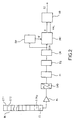
- Figure 1 shows an example of a system recording / playback to which the invention applies.
- the recording is done with a matrix head and reading with a magneto-optical system.
- the invention relates to other systems recording / playback.
- the support on which the information is recorded may not be a magnetic medium but can be an optical medium. It can be in the form of a disc and not of a band.
- Reading can be carried out by any known means other than a light beam, for example by a multitrack head with magneto-resistive elements.
- the system described in Figure 1 includes a support recording tape such as BD tape.
- a head MT1 matrix recording system has a head matrix elementary MT2 controlled by line selection conductors MT3 and MT4 data selection conductors. This head allows to record on the BD tape different information tracks p1, p2, ... pX.
- This TL head comprises a TL1 magneto-optical transducer, by example with Kerr effect, arranged parallel to the plane of the magnetic strip and the great length of which is transverse to the length of the strip.
- a light source TL2 illuminates with a beam of polarized light and through a TL3 focusing system, the TL1 transducer in such a way that the light beam is focused substantially along a line on a face of the TL1 transducer near the BD magnetic strip.
- the beam reflected by the TL1 transducer has its polarization changed to function of the magnetic field on the tape.
- the reflected beam is transmitted by a TL4 focusing system and a tracking system TL5 to a TL6 optoelectronic detector.
- the TL6 detector is a device charge transfer photosensitive consisting of a photosensitive zone and a non-photosensitive area.
- the photosensitive area is then preferably consisting of a linear array of Np pixels and the area non-photosensitive of a reading register consisting of transfer stages.
- the charges generated in a pixel of the photosensitive area are collected in a transfer stage of the reading register.
- the detector TL6 has at least as many pixels as there are tracks on the tape.
- the TL1 transducer reflects a beam towards the TL6 detector actually made up of a set of track reading beams, each having had its polarization influenced by a track of the magnetic strip. All of these reading beams are received by the TL6 detector which thus makes it possible to detect the information read on each track of the strip BD.
- the information read may have been saved at the same time. It can also be information recorded in a time-shifted manner. Preferably, the information read is sampled at a frequency F e greater than the frequency Fbit with which it was written on the tape BD.
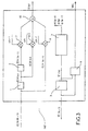
- FIG. 2 represents a block diagram of the principle of device of the invention.
- the reading register RL of the detector TL6 has been shown in FIG. 2.
- the reading register RL consists of a succession of N p transfer stages ET1, ET2, ...., ETNp .
- the output circuit CS of the read register consists of a charge-voltage converter comprising a read diode and a first read amplifier not shown in the figure.
- the signal from the CS output circuit consists of a train serial information.
- the signal from the CS output passes successively through a second amplifier AL reading, an analog-digital CAD converter, a high-pass IF filter, an EQ equalizer and a CR corrector.
- the CR corrector is a circuit correcting the crosstalk existing between a pixel and the two neighboring pixels surrounding this pixel.
- the CR corrector can be, for example, such as that described in the patent application filed in France on behalf of Plaintiffs on December 22, 1992 and registered under number 92 15474.
- the information read simultaneously by the TL1 transducer are the same information rank k contained on the X parallel tracks.
- Digital operators such that the high-pass filter FI, the equalizer EQ and the corrector CR, have then as many delay circuits as necessary so that the successive samples they process represent the information successive of the same track.
- the signal read is a series of samples whose phases are discretized. We therefore do not necessarily have samples whose phase is equal to ⁇ .
- the device of the invention consists in calculating by interpolation, for each sample, a new sample whose phase is equal to ⁇ using neighboring samples of the same track.
- the device according to the invention makes it possible to minimize the error probabilities of reading because, during decoding, the amplitude of the detected signal is calculated at its optimal phase. It follows that the invention is particularly advantageous for signals carried in high density or high speed channels having weak signal-to-noise ratios.
- the rate of writing of the binary information, commonly called bits, contained on the same track defines the frequency Fbit.
- the samples are taken at the sampling frequency F e greater than Fbit and the ratio of F e to Fbit defines the oversampling factor.
- each ECH sample from the CR corrector is sent simultaneously to a DP phase monitoring circuit and to a INT interpolator.
- phase monitoring circuit DP The function of the phase monitoring circuit DP is to estimate the phase ⁇ of the ECH sample. Estimated phase information ⁇ is sent to the INT interpolator.
- the INT interpolator therefore receives the amplitude and the estimated phase of each ECH sample.
- the function of the INT interpolator is to calculate by interpolation the value I at assign to the sample of rank k from the value of the sample ECH (k) of rank k and of sample values which surround the sample ECH (k) on the same track.
- the INT interpolator also allows the calculation of a validation signal VAL associated with the interpolated sample I and making it possible to validate or invalidate the sample I.
- VAL a validation signal associated with the interpolated sample I
- the interpolated sample I as well as the validation signal VAL which associated with it are then sent to a sorting operator TR which has for function of sorting the samples I so as to keep only those which are validated.
- the signal SI obtained at the output of the operator TR is then either consisting of the succession of validated bits, or consisting of succession of words grouping the bits validated by packets as is described in figure 4.
- FIG. 3 represents a block diagram of the principle of the interpolator shown in Figure 2.
- the calculation of interpolation of the sample I (k) of rank k is carried out using the three sampled values ECH (k-1), ECH (k) and ECH (k + 1). More general the invention however relates to the embodiments for which the calculation of the interpolated sample I (k) is carried out using i + j + 1 samples ECH (k-i), ECH (k- (i-1)), ..., ECH (k), ..., ECH (k + j) where i and j are whole numbers can be equal or not.
- the interpolator in Figure 3 includes three delay operators 1,2,3.
- the delay operator 1 contains X samples and allows return at its output the sample ECH (k - 1) of rank k when it receives at its input sample ECH (k + 1) of rank k + 1.
- the delay operator 2 whose input is connected to the output of delay operator 1, contains X samples and allows return the sample ECH (k-1) at its output when its input receives the ECH sample (k).
- the interpolated sample I (k) of rank k is calculated using the Lagrange interpolation law.
- Lagrange interpolation law a law of interpolation, based on different optimization criteria may also be suitable.
- I (k) a k-1 ECH (k-1) + a k ECH (k) + a k + 1 SAM (k + 1).
- the samples ECH (k-1), ECH (k) and ECH (k + 1) are sent to the respective multipliers 7, 8 and 9, which have the function of carrying out the respective multiplications of ECH (k -1) with a k-1 , of ECH (k) with a k and of ECH (k + 1) with a k + 1 .
- the results from the three multipliers 7, 8 and 9 are then sent to a summator 10 so as to calculate the interpolated sample I (k).
- the values of the coefficients a k-1 , a k and a k + 1 depend on the chosen interpolation law. Their values are selected according to the value of the phase ⁇ (k) of the sample of rank k.
- phase ⁇ (k) appears at the output of the delay operator 3 when the latter receives on its input the phase ⁇ (k + 1) of the sample of rank k + 1.
- phase ⁇ (k) is then sent to the search operator of phase segment 4.
- Phase ⁇ (k) has its value in the interval [0.2 ⁇ ].
- the interval [0.2 ⁇ ] is divided into N segments of phase of width 2 ⁇ / N.
- N is chosen equal to 8.
- the invention however concerns other values of N chosen preferentially the higher the lower the oversampling factor.
- the phase ⁇ (k) belongs to one of the N phase segments.
- Each phase segment is associated with a set of three precalculated values for the coefficients a k-1 , a k and a k + 1 .
- the phase segment search operator therefore also has the function of assigning to the interpolation calculation of the sample I (k) the values of the coefficients associated with the phase segment to which the phase ⁇ (k) belongs.
- the values of the coefficients a k-1 , a k and a k + 1 are taken from a table.
- This table can be, for example, a PROM type memory.
- the interpolation calculation of I (k) is then performed in real time.
- the samples ECH (k-1), ECH (k) and ECH (k + 1) are respectively multiplied, in real time, with the coefficients a k-1 , a k , and a k + 1 .
- the multiplications of the samples ECH (k-1), ECH (k) and ECH (k + 1) by the respective coefficients a k-1 , a k and a k + 1 are carried out beforehand. For each phase segment each of the possible sample values is then multiplied beforehand with each of the coefficients a k-1 , a k and a k + 1 . According to this embodiment, it is the values of the samples as well as the values of the phases which allow the addressing to the summator 10 of the previously calculated results.
- the sample I (k) is calculated from 3 sampled values ECH (k-1), ECH (k) and ECH (k + 1) and, preferably, the oversampling is equal to 2.
- the invention however relates to other embodiments such as, for example, that for which the interpolation is made from five successive samples with a factor of oversampling equal to 1.5.
- Ne samples for Nbits bits Oversampling produces on average Ne samples for Nbits bits.
- This information is generated by the validation operator 6.
- the validation operator 6 receives as input the phase ⁇ (k) of the sample of rank k and the phase ⁇ (k + 1) of the sample of rank k + 1.
- the average phase difference between two successive samples is equal to 2 ⁇ Fbit / Fe.
- the validation operator 6 compares the values of the phases ⁇ (k) and ⁇ (k + 1) at the upper limit of the validation window by extending the value of ⁇ (k + 1) on the segment [0.4 ⁇ ] if necessary.
- the VAL information takes a value signifying that the calculated sample I (k) must be validated.
- the VAL information takes a value signifying that the sample calculated I (k) must not be validated.
- the comparison constraint on a single terminal allows guarantee validation of a sample even in the presence of changes of information rhythm due, for example, to variations in the speed of tape scrolling.
- the information obtained from the sort operator can be consisting of the only succession of validated bits.
- the sort operator is then made up a memory operating at the rate of the validation signal.
- the information obtained from the sort operator can be also made up of a succession of words grouping the bits validated by packets as described in Figure 4.
- the sort operator TR then consists of y multiplexers MUX1, MUX2, ..., MUXy, and of shift registers.
- Each multiplexer has three poles P1, P2, P3 and one command input C. Under the action of a command applied to C, the link is established either between the poles P1 and P3, or between the poles P2 and P3.
- Each multiplexer has its P3 and P2 poles connected respectively to the entry and exit of a shift register.
- Each shift register contains X stages, X being the number of tracks read.
- the outputs of the shift registers constitute, in addition, a data bus B.
- the control inputs C of all the multiplexers are connected to each other and to the validation signal VAL.
- the validation signal is applied simultaneously to all the C commands of the multiplexers.
- the VAL signal must validate the sample I (k)
- a word of y bits is constituted by the information stored in the y output stages of the y shift registers.
- a synchronized counting device for the number of bits stored for each track guarantees the completeness of the reconstructed word. This word is then retrieved on the data bus B.
- An advantage of the invention is to work at a frequency which is not the frequency Fbits.
- the optoelectronic detector TL6 is a charge transfer device whose register reading includes only one output circuit.
- the register of reading the TL6 optoelectronic detector can have several outputs.
- FIG. 5 represents a first application of the device according to the invention for which the reading register comprises two outputs.
- the reading register is split in a manner known per se into a so-called “even” register and a so-called register “odd”.
- the even register collects the charges accumulated in the pixels of even rank of the photosensitive zone and the odd register recovers the charges accumulated in the odd rank pixels of the area photosensitive.
- a DI device rearranges Sla and Slb signals from respective sort operators TRa and TRb.
- Figure 6 shows a second application of the device according to the invention for which the read register comprises a number Q of outputs.
- the reading register RL consists of Q sub-registers (R1, R2, ..., Rj, ..., RQ) and each sub-register includes M transfer stages.
- M has been chosen, by way of example, equal to 6.
- the device according to the invention however relates to other modes where M is any integer that can be different for two different sub-registers.
- the M transfer stages of each sub-register Rj follow one another so that the transfer of charges is carried out from the stage of row 1 towards the stage of row M.
- the reading diode of the load-voltage converter of the sub-register Rj of rank j is integrated in the transfer stage of rank M of the sub-register Ri. This floor of transfer is denoted ESj in FIG. 6 and will subsequently be called the stage of intermediate outlet.
- the charge-voltage converter of each sub-register Rj is generally made up of the read diode contained in the output stage intermediate ESj and a first reading amplifier Aj which may or may not, in whole or in part, be integrated into the component to which the registry belongs reading.
- an MOS transistor preloads the capacity of the diode before the arrival of the charge conveyed in the sub-register Rj.
- the signals SI1 SI2, ..., SIj, ..., SIQ from the respective sorting operators TR1, TR2, ..., TRj, ..., TRQ are rearranged in a DI device.
- FIG. 7 represents the view according to section A-A of FIG. 6.
- a fraction of the sub-register Rj is represented. of rank j as well as a fraction of the sub-register Rj + 1 of rank j + 1.
- the represented fraction of the sub-register Rj consists of a stage of ET transfer of known type and the intermediate output stage ESj.
- the represented fraction of the sub-register Rj + 1 is a fraction of the stage of ET transfer of known type which adjoins the intermediate output stage ESj.
- the transfer mode chosen is of the two-phase type.
- the invention however relates to transfer modes the number of which phases is greater than two.
- the ET transfer stage is formed in a P-doped substrate 1.
- An N-doped layer 2 covers the substrate 1 so as to constitute a buried channel.
- the layer 2 doped N consists of a succession of alternately doped regions N - doped region and N.
- N - means a doped zone N but in less proportion than an N-doped zone.
- An electrically insulating layer 3 covers the doped layer 2. The electrodes which allow the transfer are produced above the electrically insulating layer 3.
- four electrodes E1, E2, E3, E4 participate in the transfer of charges in the stage AND.
- the 4 successive electrodes E1, E2, E3, E4 respectively cover doped zones N - , N, N - , N of the buried channel 2
- the two electrodes E1 and E2 are connected to the same phase Phi1 and the two electrodes E3 and E4 are connected to the same phase Phi2.
- the phases Phi1 and Phi2 are adjusted in a known manner in order to ensure the transfer of charges from the transfer stage AND from the sub-register Rj to the intermediate output stage ESj of the same sub-register.
- the intermediate output stage ESj is also formed in the P-doped substrate 1.
- the intermediate output stage successively comprises: two electrodes E6 and E7 connected to the same phase Phi1, an output electrode 4 to which a voltage Vg is applied, an N + doped area 5 and a P + doped area 6, the areas 5 and 6 are both formed in the substrate 1.
- the reading diode is formed by the junction between the N + doped zone and the P doped substrate 1.
- the electrodes E6 and E7 are located on the surface of the electrically insulating layer 3 and respectively cover an N-doped area - and an N-doped area of the buried channel 2.
- the electrode 4 is also located on the surface of the layer 3 and covers a N - doped area.
- the voltage Vg applied to the electrode 4 allows the transfer of the charges in the reading diode.
- Zone 6 doped P + constitutes an isolation barrier between the sub-register Rj and the sub-register Rj + 1.
- the voltage which appears at the terminals of the read diode is applied to the input of the first read amplifier Aj (not shown in the figure) via the conductive connection Kj.
- the intermediate output stage collects the charges accumulated in the pixel which adjoins it.
- the transfer of charges to the output amplifier Aj of each sub-register Ri then takes place without dead time.
- the N + doped zone 5 stretches in the direction perpendicular to the direction of propagation of the charges over the entire width of the intermediate output stage. It follows that the electric field which makes it possible to accelerate the charges towards the diode is constant. The acceleration of the charges being uniform, their transfer also takes place uniformly and, therefore, faster than in the read registers of known type.
- Figure 8 shows the sectional view A-A of Figure 6 of a second embodiment of the reading register.
- figure 8 represents a fraction of the sub-register Rj of rank j as well as a fraction of the sub-register Rj + 1 of rank j + 1.
- the transfer mode chosen is of the two-phase type, but, as has been mentioned previously, the invention also relates to modes of transfer whose number of phases is greater than two.
- the ET transfer stages represented in FIG. 8 are identical to those represented in FIG. 7. The same is true of the intermediate output stage ESj except with regard to the element making it possible to constitute the insulation barrier between the sub -register Rj and the sub-register Rj + 1.
- the insulation barrier is produced by an electrode 7 to which a potential Vi is applied.
- the electrode 7 is located on the surface of the layer 3 and covers an N - doped area.
- the use of a photosensitive device such that that described in FIG. 6 makes it possible to provide very information rates high.
- the use of an TL6 optoelectronic detector having 1024 pixels and 32 outputs and used for reading a strip of 1,000 tracks provides an information flow of the order of several hundred Mbits per second.
Description
L'invention concerne un procédé de lecture de support d'enregistrement ainsi qu'un dispositif appliquant un tel procédé.A method of reading media recording device and a device applying such a method.
L'invention s'applique notamment à la lecture d'enregistrements magnétiques ou optiques et, plus particulièrement, à la lecture d'enregistrements à haute densité. Elle trouve une application préférentielle dans les systèmes d'enregistrements tels que les périphériques informatiques et tous systèmes professionnels.The invention is particularly applicable to the reading of recordings magnetic or optical and, more particularly, reading high density recordings. It finds a preferential application in recording systems such as peripherals IT and all professional systems.
Dans un enregistreur numérique, le décodage des informations binaires passe par la régénération du signal de référence temporelle, appelé signal d'horloge, qui a servi à l'enregistrement des informations. Ce signal d'horloge est le plus souvent réalisé par un oscillateur contrôlé en tension (VCO : Voltage Controlled Oscillator) inséré dans une boucle à verrouillage de phase (PLL : Phase Locked Loop) qui se synchronise sur les transitions du signal de lecture.In a digital recorder, decoding information binary goes through the regeneration of the time reference signal, called clock signal, which was used to record information. This signal clock is most often achieved by a voltage controlled oscillator (VCO: Voltage Controlled Oscillator) inserted in a locking loop phase (PLL: Phase Locked Loop) which synchronizes on the transitions of the read signal.
Dans un enregistreur multi-pistes, il est possible d'utiliser un seul signal d'horloge reconstruit pour l'ensemble des pistes, à condition que la synchronisation entre toutes les pistes inscrites sur la bande soit conservée.In a multi-track recorder, it is possible to use only one reconstructed clock signal for all tracks, provided that the synchronization between all the tracks written on the tape is kept.
Ceci suppose que les têtes d'enregistrement et les têtes de lecture soient alignées, et que la bande ne se déforme pas. Si ces conditions ne sont pas strictement respectées, les références temporelles des diverses pistes se décalent les unes par rapport aux autres, c'est le phénomène de glissement connu de l'homme de l'art sous la dénomination "skew".This assumes that the recording heads and the recording heads the readings are aligned, and that the strip does not deform. If these conditions are not strictly observed, time references of the various tracks are offset with respect to each other, this is the slip phenomenon known to those skilled in the art under the name "Skew".
Dans le cas où les informations binaires sont contenues sur un grand nombre de pistes parallèles, par exemple dans le cas où le pas entre pistes parallèles est de l'ordre de 10 à 20 µm, il est pratiquement impossible de maintenir ce phénomène de glissement dans des limites acceptables. Il est alors connu de réaliser un circuit de régénération d'horloge indépendant pour chaque piste. Ceci présente de nombreux inconvénients dont, en particulier, celui d'avoir à réaliser un grand nombre de circuits.In the event that the binary information is contained on a large number of parallel tracks, for example in the case where the pitch parallel tracks is around 10 to 20 µm, it is practically impossible to keep this sliding phenomenon within acceptable limits. he it is then known to make an independent clock regeneration circuit for each track. This has many drawbacks, including in particular, that of having to carry out a large number of circuits.
L'invention ne présente pas ces inconvénients.The invention does not have these drawbacks.
L'invention a pour objet un procédé de lecture d'informations
binaires inscrites sur un support et
situées sur différentes pistes (p1,...,pX), lesdites
informations binaires ayant été inscrites sur le support à la fréquence Fbit,
caractérisé en ce qu'il comprend une étape de lecture desdites informations
binaires à la fréquence d'échantillonnage Fe supérieure à la fréquence Fbit et
lisant simultanément les informations binaires de même ordre k sur les
différentes pistes de façon à constituer une succession d'échantillons lus
successifs ECH (k) pour chaque piste, ECH (k) étant l'échantillon lu d'ordre k,
chaque échantillon lu d'ordre k ayant sa phase ϕ(k) comprise entre 0 et 2π,
une étape d'interpolation permettant de calculer un échantillon interpolé I(k)
de phase égale à π correspondant à l'échantillon lu ECH(k), à partir de
l'échantillon lu ECH (k) et des i + j échantillons lus (ECH(k-i), ... , ECH (k+j))
sur la même piste et qui encadrent l'échantillon lu ECH(k) de façon que :
La présente invention a aussi pour objet un système de lecture d'information binaires inscrites sur un support magnétique et situées sur différentes pistes (p1,..., pX), lesdites informations binaires ayant été inscrites sur le support à la fréquence Fbit, comprenant :
- des moyens de lecture permettant de lire lesdites informations binaires à une fréquence d'échantillonnage Fe supérieure à la fréquence Fbit et lisant simultanément les informations binaires de même rang k sur les différentes pistes de façon à obtenir une succession d'échantillons lus successifs ECH(k) pour chaque piste, k étant le rang de l'échantillon ECH(k) sur chaque piste ;
- des moyens d'interpolation permettant de calculer un échantillon
interpolé I(k) pour chaque échantillon lu ECH(k) à partir de l'échantillon
ECH(k) et des i + j échantillons lus qui encadrent l'échantillon ECH(k) sur la
même piste de façon que :
- reading means making it possible to read said binary information at a sampling frequency F e greater than the frequency Fbit and simultaneously reading binary information of the same rank k on the different tracks so as to obtain a succession of successive read samples ECH ( k) for each track, k being the rank of the ECH sample (k) on each track;
- interpolation means making it possible to calculate an interpolated sample I (k) for each sample read ECH (k) from the sample ECH (k) and from the i + j samples read which surround the sample ECH (k) on the same track so that:
Un avantage de l'invention est d'éviter la multiplication des circuits de régénération d'horloge et des circuits de décodage des informations binaires.An advantage of the invention is to avoid the multiplication of clock regeneration circuits and decoding circuits for binary information.
D'autres caractéristiques et avantages de l'invention apparaítront à la lecture d'un mode de réalisation préférentiel fait avec référence aux figures ci-annexées parmi lesquelles :
- la figure 1 représente un exemple de système d'enregistrement/lecture auquel s'applique l'invention ;
- la figure 2 représente un schéma synoptique de principe du dispositif de l'invention ;
- la figure 3 représente un schéma synoptique de l'interpolateur (INT) représenté en figure 2 ;
- la figure 4 représente un schéma synoptique de l'opérateur de tri (TR) représenté en figure 2 ;
- la figure 5 représente une première application du dispositif selon l'invention ;
- la figure 6 représente une deuxième application du dispositif selon l'invention ;
- la figure 7 représente la vue selon la coupe A-A de la figure 6 d'un premier mode de réalisation de la deuxième application ;
- la figure 8 représente la vue selon la coupe A-A de la figure 6 d'un deuxième mode de réalisation de la deuxième application.
- FIG. 1 represents an example of a recording / playback system to which the invention applies;
- FIG. 2 represents a block diagram of the device of the invention;
- FIG. 3 represents a block diagram of the interpolator (INT) represented in FIG. 2;
- FIG. 4 represents a block diagram of the sorting operator (TR) represented in FIG. 2;
- FIG. 5 represents a first application of the device according to the invention;
- FIG. 6 represents a second application of the device according to the invention;
- Figure 7 shows the view along section AA of Figure 6 of a first embodiment of the second application;
- Figure 8 shows the view along section AA of Figure 6 of a second embodiment of the second application.
Sur toutes les figures, les mêmes repères désignent les mêmes éléments.In all the figures, the same references designate the same elements.
La figure 1 représente un exemple de système d'enregistrement/lecture auquel s'applique l'invention. L'enregistrement se fait avec une tête matricielle et la lecture avec un système magnéto-optique. De façon plus générale, l'invention concerne d'autres systèmes d'enregistrement/lecture. Pour ces autres systèmes, le support sur lequel l'information est enregistrée peut ne pas être un support magnétique mais peut être un support optique. Il peut se présenter sous la forme d'un disque et non pas d'une bande. La lecture peut être réalisée par tout moyen connu autre qu'un faisceau lumineux, par exemple par une tête multipiste à éléments magnéto-résistifs.Figure 1 shows an example of a system recording / playback to which the invention applies. The recording is done with a matrix head and reading with a magneto-optical system. More generally, the invention relates to other systems recording / playback. For these other systems, the support on which the information is recorded may not be a magnetic medium but can be an optical medium. It can be in the form of a disc and not of a band. Reading can be carried out by any known means other than a light beam, for example by a multitrack head with magneto-resistive elements.
Le système décrit en figure 1 comporte un support d'enregistrement tel qu'une bande magnétique BD. Une tête d'enregistrement matricielle MT1 comporte une matrice de têtes élémentaires MT2 commandée par des conducteurs de sélection de lignes MT3 et des conducteurs de sélection de données MT4. Cette tête permet d'enregistrer sur la bande BD différentes pistes d'informations p1, p2, ... pX.The system described in Figure 1 includes a support recording tape such as BD tape. A head MT1 matrix recording system has a head matrix elementary MT2 controlled by line selection conductors MT3 and MT4 data selection conductors. This head allows to record on the BD tape different information tracks p1, p2, ... pX.
Sur la partie droite de la figure, on a représenté une tête de lecture magnéto-optique TL telle que celle décrite dans la demande de brevet français n° 89 17313 déposée le 28 novembre 1989 au nom de THOMSON CONSUMER ELECTRONICS.On the right side of the figure, a head of TL magneto-optical reading such as that described in the request for French patent n ° 89 17313 filed on November 28, 1989 in the name of THOMSON CONSUMER ELECTRONICS.
Cette tête TL comporte un transducteur magnéto-optique TL1, par exemple à effet Kerr, disposé parallèlement au plan de la bande magnétique et dont la grande longueur est transverse à la longueur de la bande. Une source lumineuse TL2 éclaire, par un faisceau de lumière polarisée et à travers un système de focalisation TL3, le transducteur TL1 de telle façon que le faisceau lumineux soit focalisé sensiblement selon une ligne sur une face du transducteur TL1 à proximité de la bande magnétique BD. Le faisceau réfléchi par le transducteur TL1 voit sa polarisation modifiée en fonction du champ magnétique sur la bande. Le faisceau réfléchi est transmis par un système de focalisation TL4 et un système de suivi de piste TL5 à un détecteur optoélectronique TL6.This TL head comprises a TL1 magneto-optical transducer, by example with Kerr effect, arranged parallel to the plane of the magnetic strip and the great length of which is transverse to the length of the strip. A light source TL2 illuminates with a beam of polarized light and through a TL3 focusing system, the TL1 transducer in such a way that the light beam is focused substantially along a line on a face of the TL1 transducer near the BD magnetic strip. The beam reflected by the TL1 transducer has its polarization changed to function of the magnetic field on the tape. The reflected beam is transmitted by a TL4 focusing system and a tracking system TL5 to a TL6 optoelectronic detector.
De façon préférentielle, le détecteur TL6 est un dispositif photosensible à transfert de charges constitué d'une zone photosensible et d'une zone non photosensible. La zone photosensible est alors préférentiellement constituée d'une barrette linéaire de Np pixels et la zone non photosensible d'un registre de lecture constitué d'étages de transfert. Les charges générées dans un pixel de la zone photosensible sont recueillies dans un étage de transfert du registre de lecture. Le détecteur TL6 comprend au moins autant de pixels qu'il y a de pistes sur la bande.Preferably, the TL6 detector is a device charge transfer photosensitive consisting of a photosensitive zone and a non-photosensitive area. The photosensitive area is then preferably consisting of a linear array of Np pixels and the area non-photosensitive of a reading register consisting of transfer stages. The charges generated in a pixel of the photosensitive area are collected in a transfer stage of the reading register. The detector TL6 has at least as many pixels as there are tracks on the tape.
Le transducteur TL1 réfléchit vers le détecteur TL6 un faisceau constitué en réalité d'un ensemble de faisceaux de lecture de pistes, chacun ayant eu sa polarisation influencée par une piste de la bande magnétique. L'ensemble de ces faisceaux de lecture est reçu par le détecteur TL6 qui permet ainsi de détecter les informations lues sur chaque piste de la bande BD.The TL1 transducer reflects a beam towards the TL6 detector actually made up of a set of track reading beams, each having had its polarization influenced by a track of the magnetic strip. All of these reading beams are received by the TL6 detector which thus makes it possible to detect the information read on each track of the strip BD.
Lorsque la bande défile dans le sens indiqué par la flèche FL, le transducteur magnéto-optique TL1 lit simultanément les informations binaires de même rang R (R = 1, 2, ... , k-1, k, k+1, ...) situées sur les X pistes parallèles p1, p2, ... , pX.When the strip runs in the direction indicated by the arrow FL, the TL1 magneto-optical transducer reads information simultaneously binaries of the same rank R (R = 1, 2, ..., k-1, k, k + 1, ...) located on the X parallel tracks p1, p2, ..., pX.
Les informations lues peuvent avoir été enregistrées au même instant. Il peut aussi s'agir d'informations enregistrées de façon décalée dans le temps. Préférentiellement, les informations lues sont échantillonnées à une fréquence Fe supérieure à la fréquence Fbit avec laquelle elles ont été inscrites sur la bande BD.The information read may have been saved at the same time. It can also be information recorded in a time-shifted manner. Preferably, the information read is sampled at a frequency F e greater than the frequency Fbit with which it was written on the tape BD.
La figure 2 représente un schéma synoptique de principe du dispositif de l'invention.FIG. 2 represents a block diagram of the principle of device of the invention.
Pour des raisons de commodité, seul le registre de lecture RL du détecteur TL6 a été représenté sur la figure 2. Le registre de lecture RL est constitué d'une succession de Np étages de transfert ET1, ET2, .... ,ETNp. Le circuit de sortie CS du registre de lecture est constitué d'un convertisseur charges-tension comprenant une diode de lecture et un premier amplificateur de lecture non représentés sur la figure.For reasons of convenience, only the reading register RL of the detector TL6 has been shown in FIG. 2. The reading register RL consists of a succession of N p transfer stages ET1, ET2, ...., ETNp . The output circuit CS of the read register consists of a charge-voltage converter comprising a read diode and a first read amplifier not shown in the figure.
Le signal issu du circuit de sortie CS est constitué d'un train d'informations en série. De façon connue en soi, le signal issu du circuit de sortie CS passe successivement à travers un deuxième amplificateur de lecture AL, un convertisseur analogique-digital CAD, un filtre passe-haut FI, un égaliseur EQ et un correcteur CR. Le correcteur CR est un circuit corrigeant la diaphonie existant entre un pixel et les deux pixels voisins entourant ce pixel. Le correcteur CR peut être, par exemple, tel que celui décrit dans la demande de brevet déposée en France au nom des Demanderesses le 22 décembre 1992 et enregistrée sous le numéro 92 15474. The signal from the CS output circuit consists of a train serial information. In a manner known per se, the signal from the CS output passes successively through a second amplifier AL reading, an analog-digital CAD converter, a high-pass IF filter, an EQ equalizer and a CR corrector. The CR corrector is a circuit correcting the crosstalk existing between a pixel and the two neighboring pixels surrounding this pixel. The CR corrector can be, for example, such as that described in the patent application filed in France on behalf of Plaintiffs on December 22, 1992 and registered under number 92 15474.
Comme cela a été mentionné précédemment, les informations lues simultanément par le transducteur TL1 sont les informations de même rang k contenues sur les X pistes parallèles. Les opérateurs numériques tels que le filtre passe-haut FI, l'égaliseur EQ et le correcteur CR, possèdent alors autant de circuits de retard qu'il est nécessaire de façon que les échantillons successifs qu'ils traitent représentent les informations successives d'une même piste.As mentioned earlier, the information read simultaneously by the TL1 transducer are the same information rank k contained on the X parallel tracks. Digital operators such that the high-pass filter FI, the equalizer EQ and the corrector CR, have then as many delay circuits as necessary so that the successive samples they process represent the information successive of the same track.
Dans un canal de transmission analogique, on associe au signal analogique lu x(t) une phase variant continûment de 0 à 2 π. La démodulation s'effectue généralement en observant le signe du signal x(t) à l'instant ou la phase est égale à π.In an analog transmission channel, we associate with the signal analog lu x (t) a phase varying continuously from 0 to 2 π. The demodulation is generally carried out by observing the sign of the signal x (t) at the instant when the phase is equal to π.
Dans un canal de transmission numérique, tel que celui de l'invention, le signal lu est une suite d'échantillons dont les phases sont discrétisées. On ne dispose pas alors nécessairement d'échantillons dont la phase est égale à π. Le dispositif de l'invention consiste à calculer par interpolation, pour chaque échantillon, un nouvel échantillon dont la phase est égale à π en s'aidant des échantillons voisins d'une même piste. Le dispositif selon l'invention permet de minimiser les probabilités d'erreur de lecture car, lors du décodage, l'amplitude du signal détecté est calculé à sa phase optimale. Il s'en suit que l'invention est particulièrement avantageuse pour des signaux véhiculés dans des canaux à haute densité ou à haut débit possédant des rapports signaux sur bruit faibles.In a digital transmission channel, such as that of the invention, the signal read is a series of samples whose phases are discretized. We therefore do not necessarily have samples whose phase is equal to π. The device of the invention consists in calculating by interpolation, for each sample, a new sample whose phase is equal to π using neighboring samples of the same track. The device according to the invention makes it possible to minimize the error probabilities of reading because, during decoding, the amplitude of the detected signal is calculated at its optimal phase. It follows that the invention is particularly advantageous for signals carried in high density or high speed channels having weak signal-to-noise ratios.
La cadence d'écriture des informations binaires, communément appelées bits, contenues sur une même piste définit la fréquence Fbit. Les échantillons sont prélevés à la fréquence d'échantillonnage Fe supérieure à Fbit et le rapport de Fe sur Fbit définit le facteur de suréchantillonnage.The rate of writing of the binary information, commonly called bits, contained on the same track defines the frequency Fbit. The samples are taken at the sampling frequency F e greater than Fbit and the ratio of F e to Fbit defines the oversampling factor.
Selon l'invention, chaque échantillon ECH issu du correcteur CR est envoyé simultanément dans un circuit de suivi de phase DP et dans un interpolateur INT.According to the invention, each ECH sample from the CR corrector is sent simultaneously to a DP phase monitoring circuit and to a INT interpolator.
Le circuit de suivi de phase DP a pour fonction d'estimer la phase ϕ de l'échantillon ECH. L'information de phase ϕ estimée est envoyée dans l'interpolateur INT.The function of the phase monitoring circuit DP is to estimate the phase ϕ of the ECH sample. Estimated phase information ϕ is sent to the INT interpolator.
L'interpolateur INT reçoit donc l'amplitude et la phase estimée de chaque échantillon ECH. Comme cela sera précisé en figure 3, l'interpolateur INT a pour fonction de calculer par interpolation la valeur I à affecter à l'échantillon de rang k à partir de la valeur de l'échantillon ECH(k) de rang k et de valeurs d'échantillons qui encadrent l'échantillon ECH(k) sur une même piste.The INT interpolator therefore receives the amplitude and the estimated phase of each ECH sample. As will be specified in Figure 3, the function of the INT interpolator is to calculate by interpolation the value I at assign to the sample of rank k from the value of the sample ECH (k) of rank k and of sample values which surround the sample ECH (k) on the same track.
Selon l'invention, l'interpolateur INT permet aussi le calcul d'un signal de validation VAL associé à l'échantillon interpolé I et permettant de valider ou d'invalider l'échantillon I. Le principe de cette validation est décrit en détail à la figure 3.According to the invention, the INT interpolator also allows the calculation of a validation signal VAL associated with the interpolated sample I and making it possible to validate or invalidate the sample I. The principle of this validation is described in detail in Figure 3.
L'échantillon interpolé I ainsi que le signal de validation VAL qui lui est associé sont alors envoyés dans un opérateur de tri TR qui a pour fonction de faire le tri des échantillons I de façon à ne conserver que ceux qui sont validés. Le signal SI obtenu en sortie de l'opérateur TR est alors soit constitué de la succession des bits validés, soit constitué de la succession de mots regroupant les bits validés par paquets comme cela est décrit en figure 4.The interpolated sample I as well as the validation signal VAL which associated with it are then sent to a sorting operator TR which has for function of sorting the samples I so as to keep only those which are validated. The signal SI obtained at the output of the operator TR is then either consisting of the succession of validated bits, or consisting of succession of words grouping the bits validated by packets as is described in figure 4.
La figure 3 représente un schéma synoptique de principe de l'interpolateur représenté en figure 2.FIG. 3 represents a block diagram of the principle of the interpolator shown in Figure 2.
Selon le mode de réalisation représenté en figure 3, le calcul d'interpolation de l'échantillon I(k) de rang k est effectué à l'aide des trois valeurs échantillonnées ECH(k-1), ECH(k) et ECH(k+1). De façon plus générale l'invention concerne cependant les modes de réalisation pour lesquels le calcul de l'échantillon interpolé I(k) est effectué à l'aide des i + j + 1 échantillons ECH(k-i), ECH(k-(i-1)), ... , ECH(k), ... , ECH(k+j) où i et j sont des nombres entiers pouvant être égaux ou non.According to the embodiment shown in Figure 3, the calculation of interpolation of the sample I (k) of rank k is carried out using the three sampled values ECH (k-1), ECH (k) and ECH (k + 1). More general the invention however relates to the embodiments for which the calculation of the interpolated sample I (k) is carried out using i + j + 1 samples ECH (k-i), ECH (k- (i-1)), ..., ECH (k), ..., ECH (k + j) where i and j are whole numbers can be equal or not.
L'interpolateur de la figure 3 comprend trois opérateurs de retard
1,2,3.The interpolator in Figure 3 includes three
L'opérateur de retard 1 contient X échantillons et permet de
restituer à sa sortie l'échantillon ECH(k - 1) de rang k lorsqu'il reçoit à son
entrée l'échantillon ECH (k + 1) de rang k+1.The
De même, l'opérateur de retard 2 dont l'entrée est reliée à la
sortie de l'opérateur de retard 1, contient X échantillons et permet de
restituer à sa sortie l'échantillon ECH(k-1) lorsque son entrée reçoit
l'échantillon ECH(k).Likewise, the
Selon le mode de réalisation préférentiel, l'échantillon interpolé I(k) de rang k est calculé à l'aide de la loi d'interpolation de Lagrange. De façon plus générale, cependant, d'autres lois d'interpolation, basées sur des critères d'optimisation différents peuvent également convenir.According to the preferred embodiment, the interpolated sample I (k) of rank k is calculated using the Lagrange interpolation law. Of more generally, however, other laws of interpolation, based on different optimization criteria may also be suitable.
Selon le mode de réalisation décrit en figure 3, l'échantillon
interpolé I(k) calculé s'écrit :
A cette fin, les échantillons ECH(k-1), ECH(k) et ECH(k+1) sont
envoyés sur les multiplicateurs respectifs 7, 8 et 9, lesquels ont pour
fonction d'effectuer les multiplications respectives de ECH(k-1) avec ak-1,
de ECH(k) avec ak et de ECH(k+1) avec ak+1. Les résultats issus des trois
multiplicateurs 7, 8 et 9 sont alors envoyés dans un sommateur 10 de façon
à calculer l'échantillon interpolé I(k).To this end, the samples ECH (k-1), ECH (k) and ECH (k + 1) are sent to the
Selon l'invention, les valeurs des coefficient ak-1, ak et ak+1 dépendent de la loi d'interpolation choisie. Leurs valeurs sont sélectionnées en fonction de la valeur de la phase ϕ (k) de l'échantillon de rang k.According to the invention, the values of the coefficients a k-1 , a k and a k + 1 depend on the chosen interpolation law. Their values are selected according to the value of the phase ϕ (k) of the sample of rank k.
Au sein de l'interpolateur, la phase ϕ(k) apparaít en sortie de
l'opérateur de retard 3 lorsque ce dernier reçoit sur son entrée la phase ϕ
(k+1) de l'échantillon de rang k+1.Within the interpolator, phase ϕ (k) appears at the output of
the
La phase ϕ(k) est alors envoyée dans l'opérateur de recherche de
segment de phase 4. La phase ϕ(k) a sa valeur comprise dans l'intervalle
[0,2 π]. Selon l'invention, l'intervalle [0,2 π] est divisé en N segments de
phase de largeur 2π / N. A titre d'exemple, N est choisi égal à 8. L'invention
concerne cependant d'autres valeurs de N choisies préférentiellement
d'autant plus élevées que le facteur de suréchantillonnage est faible.The phase ϕ (k) is then sent to the search operator of
La phase ϕ(k) appartient à l'un des N segments de phase. A chaque segment de phase, est associé un ensemble de trois valeurs précalculées pour les coefficients ak-1, ak et ak+1. L'opérateur de recherche de segment de phase a donc aussi pour fonction d'affecter au calcul d'interpolation de l'échantillon I(k) les valeurs des coefficients associées au segment de phase auquel appartient la phase ϕ(k).The phase ϕ (k) belongs to one of the N phase segments. Each phase segment is associated with a set of three precalculated values for the coefficients a k-1 , a k and a k + 1 . The phase segment search operator therefore also has the function of assigning to the interpolation calculation of the sample I (k) the values of the coefficients associated with the phase segment to which the phase ϕ (k) belongs.
Les valeurs des coefficients ak-1, ak et ak+1 sont prélevées dans une table. Cette table peut être, par exemple, une mémoire de type PROM. Le calcul d'interpolation de I(k) est alors effectué en temps réel. Les échantillons ECH(k-1), ECH(k) et ECH(k+1) sont respectivement multipliés, en temps réel, aux coefficients ak-1, ak, et ak+1. The values of the coefficients a k-1 , a k and a k + 1 are taken from a table. This table can be, for example, a PROM type memory. The interpolation calculation of I (k) is then performed in real time. The samples ECH (k-1), ECH (k) and ECH (k + 1) are respectively multiplied, in real time, with the coefficients a k-1 , a k , and a k + 1 .
Selon un autre mode de réalisation, les multiplications des
échantillons ECH(k-1), ECH(k) et ECH(k+1) par les coefficients respectifs
ak-1, ak et ak+1 sont effectuées au préalable. Pour chaque segment de
phase chacune des valeurs possibles d'échantillon est alors préalablement
multipliée avec chacun des coefficients ak-1, ak et ak+1. Selon ce mode de
réalisation, ce sont les valeurs des échantillons ainsi que les valeurs des
phases qui permettent l'adressage au sommateur 10 des résultats
préalablement calculés.According to another embodiment, the multiplications of the samples ECH (k-1), ECH (k) and ECH (k + 1) by the respective coefficients a k-1 , a k and a k + 1 are carried out beforehand. For each phase segment each of the possible sample values is then multiplied beforehand with each of the coefficients a k-1 , a k and a k + 1 . According to this embodiment, it is the values of the samples as well as the values of the phases which allow the addressing to the
Selon les modes de réalisation qui viennent d'être décrits, l'échantillon I(k) est calculé à partir de 3 valeurs échantillonnées ECH(k-1), ECH(k) et ECH(k+1) et, de façon préférentielle, le facteur de suréchantillonnage est égal à 2. L'invention concerne cependant d'autres modes de réalisation tel que, par exemple, celui pour lequel l'interpolation est effectuée à partir de cinq échantillons successifs avec un facteur de suréchantillonnnage égal à 1,5.According to the embodiments which have just been described, the sample I (k) is calculated from 3 sampled values ECH (k-1), ECH (k) and ECH (k + 1) and, preferably, the oversampling is equal to 2. The invention however relates to other embodiments such as, for example, that for which the interpolation is made from five successive samples with a factor of oversampling equal to 1.5.
Le suréchantillonnage produit en moyenne Ne échantillons pour Nbits bits. Le calcul d'interpolation conduit au calcul de Ne échantillons I(k). Parmi les échantillons I(k) seuls doivent être retenus les Nbits à affecter aux bits. Il est alors nécessaire que chaque échantillon I(k) s'accompagne d'une information permettant de le valider ou de l'invalider.Oversampling produces on average Ne samples for Nbits bits. The interpolation calculation leads to the calculation of Ne samples I (k). Among the samples I (k) only must be retained the Nbits to be assigned to bits. It is then necessary that each sample I (k) is accompanied by a information to validate or invalidate it.
Cette information, notée VAL sur la figure 4, est générée par
l'opérateur de validation 6.This information, denoted VAL in FIG. 4, is generated by
the
L'opérateur de validation 6 reçoit en entrée la phase ϕ(k) de
l'échantillon de rang k et la phase ϕ(k+1) de l'échantillon de rang k+1. La
différence de phase moyenne entre deux échantillons successifs est égale à
2π Fbit / Fe.The
II est alors possible de définir, autour de la phase π désirée, une fenêtre de validation allant de π - π Fbit / Fe à π + π Fbit / Fe.It is then possible to define, around the desired phase π, a validation window ranging from π - π Fbit / Fe to π + π Fbit / Fe.
L'opérateur de validation 6 compare les valeurs des phases ϕ(k)
et ϕ(k+1) à la borne supérieure de la fenêtre de validation en prolongeant la
valeur de ϕ(k+1) sur le segment [0,4 π] si nécessaire. The
Si la borne supérieure π + π Fbit / Fe appartient à l'intervalle [ϕ(k), ϕ(k + 1)[, l'information VAL prend une valeur signifiant que l'échantillon calculé I(k) doit être validé.If the upper bound π + π Fbit / Fe belongs to the interval [ϕ (k), ϕ (k + 1) [, the VAL information takes a value signifying that the calculated sample I (k) must be validated.
Si la borne supérieure π + π Fbit / Fe n'appartient pas à l'intervalle {ϕ (k), ϕ(k + 1)[, l'information VAL prend une valeur signifiant que l'échantillon calculé I(k) ne doit pas être validé.If the upper bound π + π Fbit / Fe does not belong to the interval {ϕ (k), ϕ (k + 1) [, the VAL information takes a value signifying that the sample calculated I (k) must not be validated.
La contrainte de comparaison sur une seule borne permet de garantir une validation d'un échantillon même en présence de changements de rythme d'information dus, par exemple, à des variations de vitesse de défilement de bande.The comparison constraint on a single terminal allows guarantee validation of a sample even in the presence of changes of information rhythm due, for example, to variations in the speed of tape scrolling.
L'information obtenue en sortie de l'opérateur de tri peut être constituée de la seule succession des bits validés. Dans le cas, par exemple, de la lecture d'une seule piste, l'opérateur de tri est alors constitué d'une mémoire opérant au rythme du signal de validation.The information obtained from the sort operator can be consisting of the only succession of validated bits. In the case, by example, from reading a single track, the sort operator is then made up a memory operating at the rate of the validation signal.
L'information obtenue en sortie de l'opérateur de tri peut être aussi constituée d'une succession de mots regroupant les bits validés par paquets comme cela est décrit en figure 4.The information obtained from the sort operator can be also made up of a succession of words grouping the bits validated by packets as described in Figure 4.
Pour former un mot de y bits, y étant un nombre entier par exemple égal à 10, l'opérateur de tri TR est alors constitué de y multiplexeurs MUX1, MUX2, ..., MUXy, et de y registres à décalage.To form a word of y bits, y being an integer by example equal to 10, the sort operator TR then consists of y multiplexers MUX1, MUX2, ..., MUXy, and of shift registers.
Chaque multiplexeur comprend trois pôles P1, P2, P3 et une entrée de commande C. Sous l'action d'une commande appliquée à C, la liaison s'établit soit entre les pôles P1 et P3, soit entre les pôles P2 et P3.Each multiplexer has three poles P1, P2, P3 and one command input C. Under the action of a command applied to C, the link is established either between the poles P1 and P3, or between the poles P2 and P3.
Chaque multiplexeur a ses pôles P3 et P2 reliés respectivement à
l'entrée et à la sortie d'un registre à décalage. Chaque registre à décalage
contient X étages, X étant le nombre de pistes lues. Le pôle P1 du
multiplexeur de rang 1, MUX1, reçoit le signal interpolé I(k) et le pôle P1 du
multiplexeur de rang x supérieur à 1 (x = 2, ..., y) est relié au pôle P2 du
multiplexeur de rang x-1. Les sorties des y registres à décalage constituent,
par ailleurs, un bus de données B. Les entrées de commande C de tous les
multiplexeurs sont reliées entre elles et au signal de validation VAL.Each multiplexer has its P3 and P2 poles connected respectively to
the entry and exit of a shift register. Each shift register
contains X stages, X being the number of tracks read. The P1 pole of
A chaque coup d'horloge, c'est-à-dire au rythme de la fréquence
d'échantillonnage Fe, le signal de validation est appliqué simultanément à
toutes les commandes C des multiplexeurs. Quand le signal VAL doit valider
l'échantillon I(k), la liaison s'établit entre les pilles P1 et P3 de chaque
multiplexeur. Il s'en suit que l'échantillon I(k) validé accède au registre à
décalage de rang 1, alors que chaque registre à décalage de rang x
supérieur à 1 (x = 2, ... , y) reçoit, en moyenne, sur son entrée l'information
issue du registre à décalage de rang x-1. Au bout d'un nombre de coups
d'horloge égal à y fois le facteur de suréchantillonnage, un mot de y bits est
constitué par l'information stockée dans les y étages de sortie des y
registres à décalage. Un dispositif de comptage synchronisé du nombre de
bits stockés pour chaque piste garantit l'intégralité du mot reconstitué. Ce
mot est alors récupéré sur le bus de données B.At each clock stroke, that is to say at the rate of the frequency
sampling signal Fe, the validation signal is applied simultaneously to
all the C commands of the multiplexers. When the VAL signal must validate
the sample I (k), the connection is established between the cells P1 and P3 of each
multiplexer. It follows that the validated sample I (k) accesses the register at
Un avantage de l'invention est de travailler à une fréquence qui n'est pas la fréquence Fbits.An advantage of the invention is to work at a frequency which is not the frequency Fbits.
Selon le mode de réalisation décrit en figure 2, le détecteur optoélectronique TL6 est un dispositif à transfert de charges dont le registre de lecture ne comprend qu'un seul circuit de sortie.According to the embodiment described in FIG. 2, the optoelectronic detector TL6 is a charge transfer device whose register reading includes only one output circuit.
Selon d'autres modes de réalisation, cependant, le registre de lecture du détecteur optoélectronique TL6 peut avoir plusieurs sorties. Avantageusement, il est alors possible d'évacuer les charges contenues dans le registre de lecture à haut débit.According to other embodiments, however, the register of reading the TL6 optoelectronic detector can have several outputs. Advantageously, it is then possible to remove the charges contained in the high speed read register.
La figure 5 représente une première application du dispositif selon l'invention pour laquelle le registre de lecture comprend deux sorties.FIG. 5 represents a first application of the device according to the invention for which the reading register comprises two outputs.
Selon cette première application, le registre de lecture est dédoublé de façon connue en soi en un registre dit "pair" et un registre dit "impair". Le registre pair récupère les charges accumulées dans les pixels de rang pair de la zone photosensible et le registre impair récupère les charges accumulées dans les pixels de rang impair de la zone photosensible.According to this first application, the reading register is split in a manner known per se into a so-called "even" register and a so-called register "odd". The even register collects the charges accumulated in the pixels of even rank of the photosensitive zone and the odd register recovers the charges accumulated in the odd rank pixels of the area photosensitive.
De façon symbolique cette division du registre de lecture en registres pair et impair a été représentée sur la figure 6 par la présence des deux sorties distinctes Sa et Sb.Symbolically this division of the reading register into even and odd registers has been represented in FIG. 6 by the presence of two separate outputs Sa and Sb.
Chacun des signaux issus des sorties respectives Sa et Sb est alors transféré dans une chaíne de lecture du type de celle décrite en figure 3. Each of the signals from the respective outputs Sa and Sb is then transferred to a reading chain of the type described in figure 3.
Afin de reconstituer dans sa continuité l'information désirée, un dispositif DI permet de réarranger les signaux Sla et Slb issus des opérateurs de tri respectifs TRa et TRb.In order to reconstitute the desired information in its continuity, a DI device rearranges Sla and Slb signals from respective sort operators TRa and TRb.
La figure 6 représente une deuxième application du dispositif selon l'invention pour laquelle le registre de lecture comprend un nombre Q de sorties.Figure 6 shows a second application of the device according to the invention for which the read register comprises a number Q of outputs.
Le registre de lecture RL est constitué de Q sous-registres (R1,
R2, ... , Rj, ... , RQ) et chaque sous-registre comprend M étages de transfert.
Pour des raisons de commodité le nombre M a été choisi, à titre d'exemple,
égal à 6. Le dispositif selon l'invention concerne cependant d'autres modes
de réalisation où M est un nombre entier quelconque pouvant être différent
pour deux sous-registres différents. Les M étages de transfert de chaque
sous-registre Rj se succèdent de façon que le transfert des charges
s'effectue de l'étage de rang 1 vers l'étage de rang M. La diode de lecture du
convertisseur charges-tension du sous-registre Rj de rang j est intégrée
dans l'étage de transfert de rang M du sous-registre Ri. Cet étage de
transfert est noté ESj sur la figure 6 et sera par la suite appelé étage de
sortie intermédiaire.The reading register RL consists of Q sub-registers (R1,
R2, ..., Rj, ..., RQ) and each sub-register includes M transfer stages.
For reasons of convenience, the number M has been chosen, by way of example,
equal to 6. The device according to the invention however relates to other modes
where M is any integer that can be different
for two different sub-registers. The M transfer stages of each
sub-register Rj follow one another so that the transfer of charges
is carried out from the stage of
Avantageusement, le registre de lecture RL est tel que les étages
de transfert des sous-registres Rj (j = 1, 2, ... , Q) se succèdent de façon que
l'étage de sortie intermédiaire ESj du sous-registre Rj jouxte l'étage de rang
1 du sous-registre Rj + 1.Advantageously, the reading register RL is such that the stages
of transfer of the sub-registers Rj (j = 1, 2, ..., Q) follow one another so that
the intermediate output stage ESj of the sub-register Rj adjoins the
Le convertisseur charges-tension de chaque sous-registre Rj est globalement constitué de la diode de lecture contenue dans l'étage de sortie intermédiaire ESj et d'un premier amplificateur de lecture Aj pouvant ou non, en tout ou partie, être intégré au composant auquel appartient le registre de lecture.The charge-voltage converter of each sub-register Rj is generally made up of the read diode contained in the output stage intermediate ESj and a first reading amplifier Aj which may or may not, in whole or in part, be integrated into the component to which the registry belongs reading.
Comme cela est connu de l'homme de l'art, un transistor MOS (non représenté sur la figure) effectue une précharge de la capacité de la diode avant l'arrivée de la charge véhiculée dans le sous-registre Rj.As is known to those skilled in the art, an MOS transistor (not shown in the figure) preloads the capacity of the diode before the arrival of the charge conveyed in the sub-register Rj.
Chacun des signaux issus des amplificateurs Aj (j = 1, 2, ... , Q) est alors transféré dans une chaíne de lecture du type de celle décrite en figure 2. Afin de reconstituer dans sa continuité l'information désirée Id, les signaux SI1 SI2, ... , SIj, ... , SIQ issus des opérateurs de tri respectifs TR1, TR2, ... , TRj, ... , TRQ sont réarrangés dans un dispositif DI. Each of the signals from the amplifiers Aj (j = 1, 2, ..., Q) is then transferred to a reading chain of the type described in figure 2. In order to reconstitute in its continuity the desired information Id, the signals SI1 SI2, ..., SIj, ..., SIQ from the respective sorting operators TR1, TR2, ..., TRj, ..., TRQ are rearranged in a DI device.
La figure 7 représente la vue selon la coupe A-A de la figure 6.FIG. 7 represents the view according to section A-A of FIG. 6.
Sur la figure 7, sont représentées une fraction du sous-registre Rj
de rang j ainsi qu'une fraction du sous-registre Rj + 1 de rang j + 1. La
fraction représentée du sous-registre Rj est constituée d'un étage de
transfert ET de type connu et de l'étage de sortie intermédiaire ESj. La
fraction représentée du sous-registre Rj + 1 est une fraction de l'étage de
transfert ET de type connu qui jouxte l'étage de sortie intermédiaire ESj.In FIG. 7, a fraction of the sub-register Rj is represented.
of rank j as well as a fraction of the sub-register Rj + 1 of
A titre d'exemple, le mode de transfert choisi est du type biphasé. L'invention concerne cependant des modes de transfert dont le nombre de phases est supérieur à deux.For example, the transfer mode chosen is of the two-phase type. The invention however relates to transfer modes the number of which phases is greater than two.
L'étage de transfert ET est formé dans un substrat 1 dopé P. Une
couche 2 dopée N recouvre le substrat 1 de façon à constituer un canal
enterré. Comme cela est connu de l'homme de l'art, en mode biphasé, la
couche 2 dopée N est constituée d'une succession de zones alternativement
dopées N- et N. Par zone dopée N- il faut entendre une zone dopée N mais
en moins forte proportion qu'une zone dopée N. Une couche électriquement
isolante 3 recouvre la couche dopée 2. Les électrodes qui permettent le
transfert sont réalisées au-dessus de la couche électriquement isolante 3.The ET transfer stage is formed in a P-doped
Selon le mode de transfert biphasé choisi comme exemple, quatre électrodes E1, E2, E3, E4 participent au transfert des charges dans l'étage ET.Depending on the two-phase transfer mode chosen as an example, four electrodes E1, E2, E3, E4 participate in the transfer of charges in the stage AND.
Dans le sens F défini comme allant du sous-registre Rj vers le
sous-registre Rj + 1, les 4 électrodes successives E1, E2, E3, E4 recouvrent
respectivement des zones dopées N-, N, N-, N du canal enterré 2. Les deux
électrodes E1 et E2 sont reliées à la même phase Phi1 et les deux
électrodes E3 et E4 sont reliées à la même phase Phi2.In the direction F defined as going from the sub-register Rj to the sub-register Rj + 1, the 4 successive electrodes E1, E2, E3, E4 respectively cover doped zones N - , N, N - , N of the buried
Les phases Phi1 et Phi2 sont ajustées de façon connue afin d'assurer le transfert des charges de l'étage de transfert ET du sous-registre Rj vers l'étage de sortie intermédiaire ESj du même sous-registre.The phases Phi1 and Phi2 are adjusted in a known manner in order to ensure the transfer of charges from the transfer stage AND from the sub-register Rj to the intermediate output stage ESj of the same sub-register.
L'étage de sortie intermédiaire ESj est aussi formé dans le
substrat 1 dopé P. Dans le sens de transfert des charges, l'étage de sortie
intermédiaire comprend successivement : deux électrodes E6 et E7 reliées à
la même phase Phi1, une électrode de sortie 4 sur laquelle est appliquée
une tension Vg, une zone 5 dopée N+ et une zone 6 dopée P+, les zones 5
et 6 étant formées toutes deux dans le substrat 1. The intermediate output stage ESj is also formed in the P-doped
La diode de lecture est formée par la jonction entre la zone dopée
N+ et le substrat 1 dopé P.The reading diode is formed by the junction between the N + doped zone and the P doped
Les électrodes E6 et E7 sont situées en surface de la couche
électriquement isolante 3 et recouvrent respectivement une zone dopée N-
et une zone dopée N du canal enterré 2. L'électrode 4 est elle aussi située
en surface de la couche 3 et recouvre une zone dopée N-. La tension Vg
appliquée sur l'électrode 4 permet le transfert des charges dans la diode de
lecture. La zone 6 dopée P+ constitue une barrière d'isolation entre le sous-registre
Rj et le sous-registre Rj + 1. La tension qui apparaít aux bornes de
la diode de lecture est appliquée à l'entrée du premier amplificateur de
lecture Aj (non représenté sur la figure) par l'intermédiaire de la connexion
conductrice Kj.The electrodes E6 and E7 are located on the surface of the electrically insulating
Lors du transfert des charges de la zone photosensible vers le registre de lecture, l'étage de sortie intermédiaire récupère les charges accumulées dans le pixel qui le jouxte. Avantageusement, le transfert des charges vers l'amplificateur de sortie Aj de chaque sous-registre Ri s'effectue alors sans temps mort.When transferring charges from the photosensitive area to the read register, the intermediate output stage collects the charges accumulated in the pixel which adjoins it. Advantageously, the transfer of charges to the output amplifier Aj of each sub-register Ri then takes place without dead time.
La zone 5 dopée N+ s'étire dans la direction perpendiculaire à la
direction de propagation des charges sur toute la largeur de l'étage
intermédiaire de sortie. Il s'en suit que le champ électrique qui permet
d'accélérer les charges vers la diode est constant. L'accélération des
charges étant uniforme, leur transfert s'effectue lui aussi uniformément et,
partant, plus rapidement que dans les registres de lecture de type connu.The N + doped
La figure 8 représente la vue la coupe A-A de la figure 6 d'un deuxième mode de réalisation du registre de lecture.Figure 8 shows the sectional view A-A of Figure 6 of a second embodiment of the reading register.
Comme la figure 7, la figure 8 représente une fraction du sous-registre
Rj de rang j ainsi qu'une fraction du sous-registre Rj + 1 de rang j +
1. Le mode de transfert choisi est du type biphasé, mais, comme cela a été
mentionné précédemment, l'invention concerne également des modes de
transfert dont le nombre de phases est supérieur à deux.Like figure 7, figure 8 represents a fraction of the sub-register
Rj of rank j as well as a fraction of the sub-register Rj + 1 of
Les étages de transfert ET représentés en figure 8 sont
identiques à ceux représentés en figure 7. Il en est de même de l'étage de
sortie intermédiaire ESj sauf en ce qui concerne l'élément permettant de
constituer la barrière d'isolation entre le sous-registre Rj et le sous-registre
Rj + 1. La barrière d'isolation est réalisée par une électrode 7 sur laquelle
est appliqué un potentiel Vi. L'électrode 7 est située en surface de la couche
3 et recouvre une zone dopé N-.The ET transfer stages represented in FIG. 8 are identical to those represented in FIG. 7. The same is true of the intermediate output stage ESj except with regard to the element making it possible to constitute the insulation barrier between the sub -register Rj and the sub-register Rj + 1. The insulation barrier is produced by an
Avantageusement, l'utilisation d'un dispositif photosensible tel que celui décrit en figure 6 permet de fournir des débits d'information très élevés. A titre d'exemple, l'utilisation d'un détecteur optoéelectronique TL6 possédant 1024 pixels et 32 sorties et utilisé pour la lecture d'une bande de 1 000 pistes fournit un débit d'informations de l'ordre de plusieurs centaines de Mbits par seconde.Advantageously, the use of a photosensitive device such that that described in FIG. 6 makes it possible to provide very information rates high. For example, the use of an TL6 optoelectronic detector having 1024 pixels and 32 outputs and used for reading a strip of 1,000 tracks provides an information flow of the order of several hundred Mbits per second.
Claims (15)
- Process for reading binary information written on a carrier and situated on various tracks (p1,... ,pX), the said binary information having been written on the carrier at the frequency Fbit, characterized in that it comprises
a step of reading the said binary information at the sampling frequency Fe greater than the frequency Fbit and simultaneously reading the binary information of like order k on the various tracks so as to construct a succession of successive samples read SAM(k) for each track, SAM(k) being the sample read of order k, each sample read of order k having its phase ϕ(k) lying between 0 and 2π,
a step of interpolation making it possible to calculate an interpolated sample I(k) of phase equal to π corresponding to the sample read SAM(k), on the basis of the sample read SAM(k) and of the i+j samples read (SAM(k-i), ..., SAM(k+j)) on the same track and which flank the sample read SAM(k) in such a way that:
the said interpolation step incorporating delay phases in such a way that the successive samples processed represent the successive information items of one and the same track. - Reading process according to Claim 1, characterized in that the validation step consists in comparing the quantity π + π with the interval [ϕ(k), ϕ(k+1) [ in such a way that the said information item (VAL) makes it possible to validate the interpolated sample I(k) if π + π belongs to the said interval or not to validate the interpolated sample I(k) if π + π does not belong to the said interval.
- Reading process according to either of Claims 1 and 2, characterized in that the values of the coefficients ak-i, ..., ak, ..., ak+j are included in tables and are selected as a function of the value of the phase ϕ(k) of the sample SAM(k).
- Reading process according to Claim 3, characterized in that the values of the said coefficients are precalculated for N phase segments which divide the interval [0, 2π] and in that the values chosen for the said coefficients are those corresponding to the phase interval to which the phase ϕ(k) of the sample SAM(k) belongs.
- Reading process according to either of Claims 1 and 2, characterized in that the values which the quantities ak-iSAM(k-i), ..., akSAM(k), ..., ak+jSAM(k+j) can take are precalculated for N phase segments which divide the interval [0, 2π], the values of the samples SAM(k-i), ..., SAM(k), ..., SAM(k+j) being taken from among all the values which can be taken by the said samples, and in that the values chosen for the said quantities are those corresponding to the value of the sample SAM(k) and to the phase interval to which the phase ϕ(k) of the sample SAM(k) belongs.
- Reading process according to any one of the preceding claims, characterized in that it comprises a step of sorting the interpolated samples according to whether the said interpolated samples are to be validated or not validated.
- Reading process according to Claim 6, characterized in that the sorting step makes it possible to group the validated interpolated samples into packets in such a way as to construct a succession of words.
- Reading process according to Claim 6, characterized in that it relates to the reading of a single track and in that the sorting step consists in storing the interpolated samples in tempo with the information item (VAL) intended to validate the interpolated samples.
- System for reading binary information written on a magnetic carrier and situated on various tracks (p1, ...,pX), the said binary information having been written on the carrier at the frequency Fbit, comprising:reading means making it possible to read the said binary information at a sampling frequency Fe greater than the frequency Fbit and simultaneously reading the binary information of like rank k on the various tracks so as to obtain a succession of successive samples read SAM(k) for each track, k being the rank of the sample SAM(k) on each track, each sample read of rank k having its phase ϕ(k) lying between 0 and 2π;means of interpolation making it possible to calculate an interpolated sample I(k) of phase equal to π for each sample read SAM(k) on the basis of the sample SAM(k) and of the i+j samples read which flank the sample SAM(k) on the same track in such a way that:means of validation making it possible to generate an information item (VAL) intended to validate or to invalidate the interpolated sample I(k),
the said interpolation means providing delay means in such a way that the successive samples processed represent successive information items of one and the same track. - Information reading system according to Claim 9, characterized in that it comprises:a magneto-optical reading head making it possible to transform into luminous information the binary information read simultaneously on at least one track at the sampling frequency Fe,a charge transfer photosensitive device gathering the said luminous information and making it possible to transform the said luminous information into a succession of voltage samples, the said photosensitive device comprising at least one output delivering the said voltage samples,delay means (1, 2) linked to the said output and making it possible to rearrange the voltage samples gathered on the said output in such a way as to obtain a succession of successive samples read SAM(k) of one and the same track, k being the rank of the sample SAM(k) on the track, interpolation means making it possible to calculate an interpolated sample I(k) for each sample read SAM(k) on the basis of the sample SAM(k) and of the i+j samples read which flank the sample SAM(k) in such a way that:
- System for reading binary information according to either of Claims 9 and 10, characterized in that the interpolation means consist of i+j+1 multipliers (7, 8, 9), each multiplier having a first input and a second input, and of a summator (10), the i+j+1 successive samples SAM(k-i), ..., SAM(k), ..., SAM(k+j) being respectively applied to the first input of the i+j+1 multipliers (7, 8, 9), the second inputs of the said multipliers receiving the respective coefficients ak-i, ..., ak, ..., ak+j, the result emanating from each multiplier being sent to the summator (10) so as to obtain the interpolated sample I(k), and in that the validation means consist of a validation operator (6) to which are sent the phase ϕ(k) of the sample read SAM(k) and the phase ϕ(k+1) of the sample read SAM(k+1) in such a way that, if the quantity π + π belongs to the interval [ϕ(k), ϕ(k+1) [, the said validation operator generates a signal (VAL) making it possible to validate the interpolated sample and, if the quantity π + π does not belong to the said interval, the said validation operator generates a signal making it possible not to validate the interpolated sample.
- Reading system according to any one of Claims 9, 10 or 11, characterized in that it comprises a sorting operator (SORT) making it possible to keep only the validated interpolated samples.
- Reading system according to any one of Claims 10 to 12, characterized in that the charge transfer photosensitive device consists of a photosensitive zone consisting of a linear array of pixels and of a nonphotosensitive zone consisting of a reading register (RL) consisting of transfer stages, the charges generated in a pixel being gathered in a transfer stage of the reading register, the reading register (RL) consisting of Q subregisters (R1, R2, ... Rj, ..., RQ), each subregister Rj comprising M transfer stages, M being any integer number which can be different for two different subregisters, the M transfer stages of each subregister following one another in such a way that the charges are transferred from the stage of rank 1 to the stage of rank M, the transfer stage of rank M of each subregister comprising a reading diode making it possible to convert the charge variations which it detects into voltage variations, each reading diode of each subregister constituting an output of the reading register (RL).
- Reading system according to either of Claims 9 and 10, characterized in that the magnetic carrier comprises several nonsynchronously readable information tracks.
- Reading process according to Claim 1, characterized in that the magnetic carrier comprises several nonsynchronously readable information tracks.
Applications Claiming Priority (3)
| Application Number | Priority Date | Filing Date | Title |
|---|---|---|---|
| FR9504820A FR2733346B1 (en) | 1995-04-21 | 1995-04-21 | METHOD FOR READING INFORMATION |
| FR9504820 | 1995-04-21 | ||
| PCT/FR1996/000601 WO1996033490A1 (en) | 1995-04-21 | 1996-04-19 | Data-reading process |
Publications (2)
| Publication Number | Publication Date |
|---|---|
| EP0766863A1 EP0766863A1 (en) | 1997-04-09 |
| EP0766863B1 true EP0766863B1 (en) | 2002-09-25 |
Family
ID=9478352
Family Applications (1)
| Application Number | Title | Priority Date | Filing Date |
|---|---|---|---|
| EP96915061A Expired - Lifetime EP0766863B1 (en) | 1995-04-21 | 1996-04-19 | Method for reading information |
Country Status (8)
| Country | Link |
|---|---|
| US (1) | US5963525A (en) |
| EP (1) | EP0766863B1 (en) |
| JP (1) | JPH10505936A (en) |
| CN (1) | CN1114915C (en) |
| DE (1) | DE69623898T2 (en) |
| DK (1) | DK0766863T3 (en) |
| FR (1) | FR2733346B1 (en) |
| WO (1) | WO1996033490A1 (en) |
Families Citing this family (7)
| Publication number | Priority date | Publication date | Assignee | Title |
|---|---|---|---|---|
| US6977875B1 (en) | 1999-07-09 | 2005-12-20 | Thales | Tracking system for recording/reading a data medium and recording medium |
| FR2797514B3 (en) * | 1999-08-10 | 2001-10-12 | Thomson Csf | MAGNETO-OPTICAL READING DEVICE FOR MULTI-TRACK MAGNETIC STRIPS |
| US6418101B1 (en) * | 1999-09-03 | 2002-07-09 | Zen Research (Ireland), Ltd. | Digital read channel for optical disk reader |
| JP3486145B2 (en) * | 2000-01-17 | 2004-01-13 | 松下電器産業株式会社 | Digital recording data playback device |
| US6693872B1 (en) * | 2000-08-29 | 2004-02-17 | Eastman Kodak Company | Multi-track optical data recording and readout |
| DE10141597B4 (en) * | 2001-08-24 | 2017-11-09 | Lantiq Deutschland Gmbh | Method for reconstructing data transmitted over a transmission link in a receiver and corresponding device |
| JP2004079015A (en) * | 2002-08-09 | 2004-03-11 | Fujitsu Ltd | Data reproducing device |
Family Cites Families (14)
| Publication number | Priority date | Publication date | Assignee | Title |
|---|---|---|---|---|
| US4707841A (en) * | 1984-08-21 | 1987-11-17 | University Of Toronto, Innovations Foundation | Digital data receiver for preamble free data transmission |
| US4780892A (en) * | 1984-10-05 | 1988-10-25 | Willi Studer Ag | Scanning frequency synchronization method and apparatus |
| NL8600931A (en) * | 1986-04-14 | 1987-11-02 | Philips Nv | METHOD AND APPARATUS FOR RESTORING INVALID SAMPLES OF AN EQUIDISTANT SAMPLED SIGNAL |
| EP0263656A3 (en) * | 1986-10-06 | 1989-11-15 | Thorn Emi Plc | Tape recording |
| GB2224911A (en) * | 1988-11-09 | 1990-05-16 | Philips Nv | Method of and apparatus for assigning binary values to sample values |
| DE69026726T2 (en) * | 1989-10-23 | 1996-11-28 | Matsushita Electric Ind Co Ltd | DIGITAL SIGNAL PLAYER WITH VARIABLE SPEED |
| JP3194752B2 (en) * | 1991-01-31 | 2001-08-06 | パイオニア株式会社 | PCM digital audio signal playback device |
| JPH0562495A (en) * | 1991-09-02 | 1993-03-12 | Pioneer Electron Corp | Sampling frequency converter |
| US5586100A (en) * | 1992-10-13 | 1996-12-17 | Literal Corporation | Transversal filter and method for cancelling intersymbol interference |
| FR2699724B1 (en) * | 1992-12-22 | 1995-01-20 | Thomson Csf | Method for reading a recording medium and system applying this method. |
| BE1007872A3 (en) * | 1993-12-15 | 1995-11-07 | Philips Electronics Nv | OPTICAL SENSING DEVICE, AND a recording and / or read EQUIPPED such a scanning device. |
| JPH07220409A (en) * | 1994-02-04 | 1995-08-18 | Pioneer Electron Corp | Digital signal reproducing device |
| JP2922113B2 (en) * | 1994-04-06 | 1999-07-19 | 松下電送システム株式会社 | Image recording device |
| US5602811A (en) * | 1994-08-11 | 1997-02-11 | Yamaha Corporation | Musical information recording and reproducing technique for use with a recording medium having a UTOC area |
-
1995
- 1995-04-21 FR FR9504820A patent/FR2733346B1/en not_active Expired - Fee Related
-
1996
- 1996-04-19 EP EP96915061A patent/EP0766863B1/en not_active Expired - Lifetime
- 1996-04-19 DK DK96915061T patent/DK0766863T3/en active
- 1996-04-19 JP JP8530789A patent/JPH10505936A/en active Pending
- 1996-04-19 US US08/750,798 patent/US5963525A/en not_active Expired - Lifetime
- 1996-04-19 DE DE69623898T patent/DE69623898T2/en not_active Expired - Lifetime
- 1996-04-19 CN CN96190371A patent/CN1114915C/en not_active Expired - Fee Related
- 1996-04-19 WO PCT/FR1996/000601 patent/WO1996033490A1/en active IP Right Grant
Also Published As
| Publication number | Publication date |
|---|---|
| CN1150857A (en) | 1997-05-28 |
| FR2733346B1 (en) | 1997-05-23 |
| EP0766863A1 (en) | 1997-04-09 |
| US5963525A (en) | 1999-10-05 |
| DE69623898T2 (en) | 2003-05-15 |
| CN1114915C (en) | 2003-07-16 |
| DK0766863T3 (en) | 2003-01-27 |
| FR2733346A1 (en) | 1996-10-25 |
| DE69623898D1 (en) | 2002-10-31 |
| WO1996033490A1 (en) | 1996-10-24 |
| JPH10505936A (en) | 1998-06-09 |
Similar Documents
| Publication | Publication Date | Title |
|---|---|---|
| FR2471109A1 (en) | DIGITAL MAGNETOSCOPE | |
| EP0627114B1 (en) | Method of reading a recording medium and system using said method | |
| FR2475828A1 (en) | METHOD AND APPARATUS FOR EXTRACTING A DIGITAL SIGNAL FROM TIME INFORMATION | |
| FR2611299A1 (en) | CUSTOM ALBUMS RECORDING SYSTEM | |
| EP0125722A1 (en) | Circuit for joint adaptive equalisation and demodulation | |
| EP0501857B1 (en) | Method and apparatus for seismic transmission at very low error rate | |
| EP0766863B1 (en) | Method for reading information | |
| EP0627113B1 (en) | Data recording medium, recorder, reader and recording method | |
| FR2685518A1 (en) | CLOCK CIRCUIT FOR SEQUENTIAL INFORMATION READING SYSTEM. | |
| EP0714091B1 (en) | Reading device and system | |
| EP0434547B1 (en) | Multitrack magnetic read head | |
| EP0295979B1 (en) | Method for writing information on a magnetic recording medium | |
| EP0094852A1 (en) | Opto-electronic method for reading information from a magnetic disc, and circuit therefor | |
| EP0718826B1 (en) | Read device and system | |
| FR2613560A1 (en) | AUTOMATIC EQUALIZER FOR DIGITAL TRANSMISSION | |
| FR2511171A1 (en) | APPARATUS AND METHOD FOR DETERMINING THE POSITION OF A READING HEAD | |
| EP0677844B1 (en) | Read system for a multitrack recording medium | |
| EP0295164B1 (en) | Method of writing synchronization information on a magnetic record carrier | |
| EP1196914B1 (en) | Tracking system for recording/reading a data medium and recording medium | |
| EP1511200A1 (en) | Device for regenerating an optical signal and corresponding method | |
| NO318778B1 (en) | Method and apparatus for reading information on a carrier, especially binary information | |
| KR100553107B1 (en) | Binary Information Reading System and Method | |
| FR2464531A1 (en) | APPARATUS AND METHOD FOR REPRODUCING DIGITAL INFORMATION RECORDED ON A MAGNETIC MEDIUM | |
| FR2779863A1 (en) | Longitudinal track following system for multitrack tape, especially for magnetic and optical recordings | |
| FR2855901A1 (en) | MULTI-TRACK OPTICAL DISC PLAYER / RECORDER |
Legal Events
| Date | Code | Title | Description |
|---|---|---|---|
| PUAI | Public reference made under article 153(3) epc to a published international application that has entered the european phase |
Free format text: ORIGINAL CODE: 0009012 |
|
| 17P | Request for examination filed |
Effective date: 19960916 |
|
| AK | Designated contracting states |
Kind code of ref document: A1 Designated state(s): DE DK FR GB IT NL SE Kind code of ref document: A1 Designated state(s): DE ES FR GB IT NL SE |
|
| RAP1 | Party data changed (applicant data changed or rights of an application transferred) |
Owner name: THOMSON MULTIMEDIA Owner name: THOMSON-CSF |
|
| 17Q | First examination report despatched |
Effective date: 19991217 |
|
| RAP1 | Party data changed (applicant data changed or rights of an application transferred) |
Owner name: THOMSON MULTIMEDIA Owner name: THALES |
|
| GRAG | Despatch of communication of intention to grant |
Free format text: ORIGINAL CODE: EPIDOS AGRA |
|
| GRAG | Despatch of communication of intention to grant |
Free format text: ORIGINAL CODE: EPIDOS AGRA |
|
| GRAH | Despatch of communication of intention to grant a patent |
Free format text: ORIGINAL CODE: EPIDOS IGRA |
|
| GRAH | Despatch of communication of intention to grant a patent |
Free format text: ORIGINAL CODE: EPIDOS IGRA |
|
| GRAA | (expected) grant |
Free format text: ORIGINAL CODE: 0009210 |
|
| RBV | Designated contracting states (corrected) |
Designated state(s): DE DK FR GB IT NL SE |
|
| AK | Designated contracting states |
Kind code of ref document: B1 Designated state(s): DE DK FR GB IT NL SE |
|
| REG | Reference to a national code |
Ref country code: GB Ref legal event code: FG4D Free format text: NOT ENGLISH |
|
| REF | Corresponds to: |
Ref document number: 69623898 Country of ref document: DE Date of ref document: 20021031 |
|
| GBT | Gb: translation of ep patent filed (gb section 77(6)(a)/1977) |
Effective date: 20021130 |
|
| REG | Reference to a national code |
Ref country code: DK Ref legal event code: T3 |
|
| PLBE | No opposition filed within time limit |
Free format text: ORIGINAL CODE: 0009261 |
|
| STAA | Information on the status of an ep patent application or granted ep patent |
Free format text: STATUS: NO OPPOSITION FILED WITHIN TIME LIMIT |
|
| 26N | No opposition filed |
Effective date: 20030626 |
|
| PGFP | Annual fee paid to national office [announced via postgrant information from national office to epo] |
Ref country code: GB Payment date: 20130424 Year of fee payment: 18 Ref country code: DE Payment date: 20130419 Year of fee payment: 18 Ref country code: DK Payment date: 20130410 Year of fee payment: 18 Ref country code: SE Payment date: 20130412 Year of fee payment: 18 |
|
| PGFP | Annual fee paid to national office [announced via postgrant information from national office to epo] |
Ref country code: NL Payment date: 20130410 Year of fee payment: 18 Ref country code: FR Payment date: 20130521 Year of fee payment: 18 Ref country code: IT Payment date: 20130422 Year of fee payment: 18 |
|
| REG | Reference to a national code |
Ref country code: DE Ref legal event code: R119 Ref document number: 69623898 Country of ref document: DE |
|
| REG | Reference to a national code |
Ref country code: DK Ref legal event code: EBP Effective date: 20140430 |
|
| REG | Reference to a national code |
Ref country code: NL Ref legal event code: V1 Effective date: 20141101 |
|
| REG | Reference to a national code |
Ref country code: SE Ref legal event code: EUG |
|
| GBPC | Gb: european patent ceased through non-payment of renewal fee |
Effective date: 20140419 |
|
| REG | Reference to a national code |
Ref country code: DE Ref legal event code: R119 Ref document number: 69623898 Country of ref document: DE Effective date: 20141101 |
|
| REG | Reference to a national code |
Ref country code: FR Ref legal event code: ST Effective date: 20141231 |
|
| PG25 | Lapsed in a contracting state [announced via postgrant information from national office to epo] |
Ref country code: DE Free format text: LAPSE BECAUSE OF NON-PAYMENT OF DUE FEES Effective date: 20141101 Ref country code: GB Free format text: LAPSE BECAUSE OF NON-PAYMENT OF DUE FEES Effective date: 20140419 Ref country code: SE Free format text: LAPSE BECAUSE OF NON-PAYMENT OF DUE FEES Effective date: 20140420 |
|
| PG25 | Lapsed in a contracting state [announced via postgrant information from national office to epo] |
Ref country code: FR Free format text: LAPSE BECAUSE OF NON-PAYMENT OF DUE FEES Effective date: 20140430 Ref country code: NL Free format text: LAPSE BECAUSE OF NON-PAYMENT OF DUE FEES Effective date: 20141101 |
|
| PG25 | Lapsed in a contracting state [announced via postgrant information from national office to epo] |
Ref country code: IT Free format text: LAPSE BECAUSE OF NON-PAYMENT OF DUE FEES Effective date: 20140419 |
|
| PG25 | Lapsed in a contracting state [announced via postgrant information from national office to epo] |
Ref country code: DK Free format text: LAPSE BECAUSE OF NON-PAYMENT OF DUE FEES Effective date: 20140430 |