EP0762285B1 - Système électronique testable - Google Patents
Système électronique testable Download PDFInfo
- Publication number
- EP0762285B1 EP0762285B1 EP96410088A EP96410088A EP0762285B1 EP 0762285 B1 EP0762285 B1 EP 0762285B1 EP 96410088 A EP96410088 A EP 96410088A EP 96410088 A EP96410088 A EP 96410088A EP 0762285 B1 EP0762285 B1 EP 0762285B1
- Authority
- EP
- European Patent Office
- Prior art keywords
- test
- board
- sub
- component
- identifier
- Prior art date
- Legal status (The legal status is an assumption and is not a legal conclusion. Google has not performed a legal analysis and makes no representation as to the accuracy of the status listed.)
- Expired - Lifetime
Links
- 238000012360 testing method Methods 0.000 claims description 87
- 239000013598 vector Substances 0.000 claims description 21
- 230000008520 organization Effects 0.000 claims description 15
- 238000000034 method Methods 0.000 claims description 8
- 230000002093 peripheral effect Effects 0.000 description 9
- 230000006399 behavior Effects 0.000 description 4
- 238000000429 assembly Methods 0.000 description 1
- 230000015572 biosynthetic process Effects 0.000 description 1
- 230000008859 change Effects 0.000 description 1
- 230000002950 deficient Effects 0.000 description 1
- 230000006870 function Effects 0.000 description 1
- 230000008569 process Effects 0.000 description 1
- 230000004044 response Effects 0.000 description 1
- 238000010998 test method Methods 0.000 description 1
Images

Classifications
-
- G—PHYSICS
- G01—MEASURING; TESTING
- G01R—MEASURING ELECTRIC VARIABLES; MEASURING MAGNETIC VARIABLES
- G01R31/00—Arrangements for testing electric properties; Arrangements for locating electric faults; Arrangements for electrical testing characterised by what is being tested not provided for elsewhere
- G01R31/28—Testing of electronic circuits, e.g. by signal tracer
- G01R31/317—Testing of digital circuits
- G01R31/3181—Functional testing
- G01R31/3185—Reconfiguring for testing, e.g. LSSD, partitioning
- G01R31/318533—Reconfiguring for testing, e.g. LSSD, partitioning using scanning techniques, e.g. LSSD, Boundary Scan, JTAG
- G01R31/318555—Control logic
-
- G—PHYSICS
- G01—MEASURING; TESTING
- G01R—MEASURING ELECTRIC VARIABLES; MEASURING MAGNETIC VARIABLES
- G01R31/00—Arrangements for testing electric properties; Arrangements for locating electric faults; Arrangements for electrical testing characterised by what is being tested not provided for elsewhere
- G01R31/28—Testing of electronic circuits, e.g. by signal tracer
- G01R31/2801—Testing of printed circuits, backplanes, motherboards, hybrid circuits or carriers for multichip packages [MCP]
- G01R31/281—Specific types of tests or tests for a specific type of fault, e.g. thermal mapping, shorts testing
- G01R31/2815—Functional tests, e.g. boundary scans, using the normal I/O contacts
-
- G—PHYSICS
- G01—MEASURING; TESTING
- G01R—MEASURING ELECTRIC VARIABLES; MEASURING MAGNETIC VARIABLES
- G01R31/00—Arrangements for testing electric properties; Arrangements for locating electric faults; Arrangements for electrical testing characterised by what is being tested not provided for elsewhere
- G01R31/28—Testing of electronic circuits, e.g. by signal tracer
- G01R31/317—Testing of digital circuits
- G01R31/3181—Functional testing
- G01R31/3185—Reconfiguring for testing, e.g. LSSD, partitioning
- G01R31/318533—Reconfiguring for testing, e.g. LSSD, partitioning using scanning techniques, e.g. LSSD, Boundary Scan, JTAG
- G01R31/318536—Scan chain arrangements, e.g. connections, test bus, analog signals
-
- G—PHYSICS
- G01—MEASURING; TESTING
- G01R—MEASURING ELECTRIC VARIABLES; MEASURING MAGNETIC VARIABLES
- G01R31/00—Arrangements for testing electric properties; Arrangements for locating electric faults; Arrangements for electrical testing characterised by what is being tested not provided for elsewhere
- G01R31/28—Testing of electronic circuits, e.g. by signal tracer
- G01R31/317—Testing of digital circuits
- G01R31/3181—Functional testing
- G01R31/3185—Reconfiguring for testing, e.g. LSSD, partitioning
- G01R31/318533—Reconfiguring for testing, e.g. LSSD, partitioning using scanning techniques, e.g. LSSD, Boundary Scan, JTAG
- G01R31/318558—Addressing or selecting of subparts of the device under test
- G01R31/318561—Identification of the subpart
Definitions
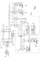
- FIG. 1 is intended to illustrate an application from the peripheral test architecture to components 10, usually logic circuits.
- Each pin 13 of components 10 is connected to the internal logic of the components via a test cell 15. Apart from the test phases, the cells 15 are transparent, that is to say that they have no influence on the signals passing through between pins 13 and the internal logic.
- all 15 cells of each component are connected to each other according to a chain which is behaves like a shift register, each cell 15 constituting a flip-flop of this shift register.
- the signal TDI corresponds to the input of the shift register and the signal TDO at the output of the shift register. So each component conforms to the standard has two pins reserved for signals TDI and TDO, but also has three additional pins reserved for the three other TMS, TCK and TRST signals.
- the peripheral test architecture also allows to test the connections between components on a printed circuit.
- the peripheral test of a component is insufficient to detect all the faults of a component. Indeed, a component can have multiple logical levels which, by successive errors, invert a data an even number of times, so that the result corresponds well to the one that is expected, while the component is defective. So by extension of the peripheral test, it is common to perform the flip-flops of a component so that they can be chained during a test phase like cells 15 for y introduce test vectors and read results.
- test vectors and expected results are conventionally obtained by exploiting in an automated manner IT plans that enabled the realization of cards or components.
Landscapes
- Engineering & Computer Science (AREA)
- General Engineering & Computer Science (AREA)
- Physics & Mathematics (AREA)
- General Physics & Mathematics (AREA)
- Computer Hardware Design (AREA)
- Microelectronics & Electronic Packaging (AREA)
- Tests Of Electronic Circuits (AREA)
Description
- chercher un composant prédéterminé en lisant les identificateurs des composants des sous-chaínes de la carte prédéterminée ; et
- tester le composant prédéterminé par l'utilisation de vecteurs de test associés, dans la base de données, à l'identificateur du composant.
Claims (8)
- Système électronique testable comprenant des éléments testables munis d'interfaces de test normalisées selon la norme IEEE 1149.1 permettant d'organiser les éléments en chaínes qui se comportent comme des registres à décalage pour assurer l'échange d'informations de test, chaque élément étant, soit un composant (10) possédant un identificateur caractéristique du comportement de test du composant et accessible par l'interface de test du composant, soit un aiguillage permettant d'organiser une chaíne en sous-chaínes individuellement sélectionnables par des canaux de l'aiguillage, caractérisé en ce qu'il comprend des aiguillages maítres (24) qui définissent des sous-ensembles (20) respectifs d'éléments, un canal spécifique de chaque aiguillage maítre, toujours le même pour un système donné, étant réservé pour accéder à un identificateur (22) caractéristique de l'organisation de test du sous-ensemble associé.
- Système électronique testable selon la revendication 1, caractérisé en ce que les canaux de chaque aiguillage maítre (24), autres que celui par lequel est accessible l'identificateur du sous-ensemble associé, sont reliés à des sous-chaínes pouvant contenir, selon une organisation quelconque, un ou plusieurs éléments ou aiguillages maítres.
- Système électronique testable selon la revendication 1, caractérisé en ce que chaque sous-ensemble correspond à une carte de circuit imprimé (20) possédant un connecteur (26) qui relie son aiguillage maítre (24) à un canal d'un aiguillage maítre d'une autre carte, toutes les cartes étant reliées, par interposition d'aiguillages maítres, à un canal d'un aiguillage maítre d'une unique carte d'interface (28) par l'intermédiaire de laquelle on effectue le test du système.
- Système électronique testable selon la revendication 3, caractérisé en ce qu'il comprend une base de données associant :à chaque identificateur distinct de composant (10), un ensemble de vecteurs de test et de résultats attendus correspondants ; età chaque identificateur (22) distinct de sous-ensemble ou de carte (20), des informations indicatives de l'organisation des sous-chaínes de la carte, un ensemble de vecteurs de test associé à chaque sous-chaíne de la carte, et des résultats attendus correspondants.
- Procédé d'exploitation d'un système électronique testable selon la revendication 4, caractérisé en ce qu'il comprend, pour tester une carte prédéterminée, l'étape consistant à parcourir le graphe constitué par les liaisons entre cartes (20) jusqu'au moment où on trouve un chemin vers la carte prédéterminée, ce parcours étant effectué en parcourant chaque carte que l'on trouve reliée à une carte précédente grâce aux informations associées, dans la base de données, à l'identificateur (22) de la carte précédente.
- Procédé d'exploitation selon la revendication 5, caractérisé en ce que le graphe est parcouru selon un chemin eulérien permettant de relier toutes les cartes (20), l'algorithme d'établissement du chemin eulérien étant modifié de manière que le chemin puisse passer plus d'une fois par un même canal.
- Procédé d'exploitation selon la revendication 5, caractérisé en ce qu'il comprend l'étape consistant à tester la carte prédéterminée par l'utilisation de vecteurs de test associés, dans la base de données, à l'identificateur (22) de la carte prédéterminée, ces vecteurs étant fournis, et les résultats correspondants lus, par le chemin trouvé.
- Procédé d'exploitation selon la revendication 5, caractérisé en ce qu'il comprend les étapes suivantes :chercher un composant prédéterminé (10) en lisant les identificateurs des composants des sous-chaínes de la carte prédéterminée ; ettester le composant prédéterminé par l'utilisation de vecteurs de test associés, dans la base de données, à l'identificateur du composant.
Applications Claiming Priority (2)
| Application Number | Priority Date | Filing Date | Title |
|---|---|---|---|
| FR9509894A FR2737782B1 (fr) | 1995-08-11 | 1995-08-11 | Systeme electronique testable |
| FR9509894 | 1995-08-11 |
Publications (2)
| Publication Number | Publication Date |
|---|---|
| EP0762285A1 EP0762285A1 (fr) | 1997-03-12 |
| EP0762285B1 true EP0762285B1 (fr) | 2001-10-31 |
Family
ID=9481976
Family Applications (1)
| Application Number | Title | Priority Date | Filing Date |
|---|---|---|---|
| EP96410088A Expired - Lifetime EP0762285B1 (fr) | 1995-08-11 | 1996-08-06 | Système électronique testable |
Country Status (4)
| Country | Link |
|---|---|
| US (1) | US5751736A (fr) |
| EP (1) | EP0762285B1 (fr) |
| DE (1) | DE69616464T2 (fr) |
| FR (1) | FR2737782B1 (fr) |
Families Citing this family (10)
| Publication number | Priority date | Publication date | Assignee | Title |
|---|---|---|---|---|
| JP3791859B2 (ja) * | 1996-10-30 | 2006-06-28 | 富士通株式会社 | ネットワークのスキャンパスを階層的に構成するスキャン装置および方法 |
| US6539510B1 (en) * | 1997-08-12 | 2003-03-25 | Xilinx, Inc. | Interface board for receiving modular interface cards |
| US6425101B1 (en) * | 1998-10-30 | 2002-07-23 | Infineon Technologies North America Corp. | Programmable JTAG network architecture to support proprietary debug protocol |
| TW484016B (en) * | 1999-07-28 | 2002-04-21 | Hitachi Ltd | Semiconductor integrated circuit and recording medium |
| US7340659B2 (en) * | 2002-05-15 | 2008-03-04 | Infineon Technologies, A.G. | Method of testing multiple modules on an integrated circuit |
| US7827510B1 (en) | 2002-06-07 | 2010-11-02 | Synopsys, Inc. | Enhanced hardware debugging with embedded FPGAS in a hardware description language |
| GB0712373D0 (en) * | 2007-06-26 | 2007-08-01 | Astrium Ltd | Embedded test system and method |
| US9940486B2 (en) * | 2015-02-23 | 2018-04-10 | Cisco Technology, Inc. | Detection of hardware tampering |
| US10572675B2 (en) | 2016-11-02 | 2020-02-25 | Cisco Technology, Inc. | Protecting and monitoring internal bus transactions |
| EP4679110A1 (fr) * | 2024-07-10 | 2026-01-14 | Mitsubishi Electric R&D Centre Europe B.V. | Procédé d'identification de défaut de carte électronique, dispositif, système et programme d'ordinateur correspondants |
Family Cites Families (3)
| Publication number | Priority date | Publication date | Assignee | Title |
|---|---|---|---|---|
| US5212785A (en) * | 1990-04-06 | 1993-05-18 | Micro Technology, Inc. | Apparatus and method for controlling data flow between a computer and memory devices |
| DE69321663T2 (de) * | 1992-06-17 | 1999-05-06 | Texas Instruments Inc., Dallas, Tex. | Hierarchisches Verbindungsverfahren, -gerät und -protokoll |
| US5333139A (en) * | 1992-12-30 | 1994-07-26 | Intel Corporation | Method of determining the number of individual integrated circuit computer chips or the like in a boundary scan test chain and the length of the chain |
-
1995
- 1995-08-11 FR FR9509894A patent/FR2737782B1/fr not_active Expired - Fee Related
-
1996
- 1996-08-06 EP EP96410088A patent/EP0762285B1/fr not_active Expired - Lifetime
- 1996-08-06 DE DE69616464T patent/DE69616464T2/de not_active Expired - Lifetime
- 1996-08-09 US US08/694,595 patent/US5751736A/en not_active Expired - Lifetime
Also Published As
| Publication number | Publication date |
|---|---|
| DE69616464T2 (de) | 2002-07-11 |
| US5751736A (en) | 1998-05-12 |
| DE69616464D1 (de) | 2001-12-06 |
| FR2737782A1 (fr) | 1997-02-14 |
| EP0762285A1 (fr) | 1997-03-12 |
| FR2737782B1 (fr) | 1997-10-31 |
Similar Documents
| Publication | Publication Date | Title |
|---|---|---|
| EP0104293B1 (fr) | Dispositif pour le chargement et la lecture de différentes chaînes de bascules dans un système de traitement de données | |
| EP0626760B1 (fr) | Système électronique organisé en réseau matriciel de cellules | |
| EP0151653B1 (fr) | Dispositif de sérialisation/désérialisation de configuration de bits de longueur variable | |
| EP0490738B1 (fr) | Circuit intégré avec contrÔleur de test périphérique | |
| EP0146661B1 (fr) | Procédé de diagnostic électrique pour identifier une cellule défectueuse dans une chaîne de cellules formant un registre à décalage | |
| EP0642683A1 (fr) | Procede et plate-formes de test pour le developpement d'un circuit integre | |
| FR2839156A1 (fr) | Circuit et procede utilisant de multiples chaines d'acces serie pour le test de cirucuits integres | |
| FR2568698A1 (fr) | Simulateur logique ayant une capacite de memoire aussi reduite que possible | |
| EP0578540B1 (fr) | Procédé pour tester le fonctionnement d'un circuit intégré spécialisé, et circuit intégré spécialisé s'y rapportant | |
| EP0762285A1 (fr) | Système électronique testable | |
| FR3066606A1 (fr) | Appareil de test et procede de test d'un circuit integre | |
| Pomeranz | Storage and counter based logic built-in self-test | |
| EP3025161B1 (fr) | Procede automatise d'analyse d'une carte portant plusieurs composants de type fpga | |
| FR2532771A1 (fr) | Procede et dispositif pour tester statiquement l'ensemble des connexions et des circuits integres peripheriques d'un microprocesseur | |
| EP1716425B1 (fr) | Procede d elaboration de fichiers de description hdl de systemes digitaux et systemes obtenus | |
| FR2846494A1 (fr) | Verification de proximite inter-signaux dans un circuit integre | |
| EP0469507A1 (fr) | Circuit intégré comprenant une cellule standard, une cellule d'application et une cellule de test | |
| EP0818686A1 (fr) | Dispositif de commutation notamment de système sous test | |
| EP1688753B1 (fr) | Sécurisation du mode de test d'un circuit intégré | |
| FR2800169A1 (fr) | Procede et dispositif d'analyse de defauts dans des circuits logiques numeriques | |
| EP0828163A1 (fr) | Circuit comprenant des moyens de test structurel sans plot de test dédié au test | |
| EP0823088B1 (fr) | Procede et equipement de test automatique en parallele de composants electroniques | |
| FR2771510A1 (fr) | Cellule de test pour circuit integre et circuit integre l'incorporant | |
| EP0803982B1 (fr) | Système électronique organisé en un réseau matriciel de cellules fonctionnelles | |
| FR2666902A1 (fr) | Circuit integre avec registre de test peripherique. |
Legal Events
| Date | Code | Title | Description |
|---|---|---|---|
| PUAI | Public reference made under article 153(3) epc to a published international application that has entered the european phase |
Free format text: ORIGINAL CODE: 0009012 |
|
| AK | Designated contracting states |
Kind code of ref document: A1 Designated state(s): DE FR GB IT |
|
| RTI1 | Title (correction) | ||
| 17P | Request for examination filed |
Effective date: 19970901 |
|
| 17Q | First examination report despatched |
Effective date: 20000529 |
|
| GRAG | Despatch of communication of intention to grant |
Free format text: ORIGINAL CODE: EPIDOS AGRA |
|
| GRAG | Despatch of communication of intention to grant |
Free format text: ORIGINAL CODE: EPIDOS AGRA |
|
| GRAH | Despatch of communication of intention to grant a patent |
Free format text: ORIGINAL CODE: EPIDOS IGRA |
|
| GRAH | Despatch of communication of intention to grant a patent |
Free format text: ORIGINAL CODE: EPIDOS IGRA |
|
| GRAA | (expected) grant |
Free format text: ORIGINAL CODE: 0009210 |
|
| AK | Designated contracting states |
Kind code of ref document: B1 Designated state(s): DE FR GB IT |
|
| REF | Corresponds to: |
Ref document number: 69616464 Country of ref document: DE Date of ref document: 20011206 |
|
| REG | Reference to a national code |
Ref country code: GB Ref legal event code: IF02 |
|
| GBT | Gb: translation of ep patent filed (gb section 77(6)(a)/1977) |
Effective date: 20020114 |
|
| PLBE | No opposition filed within time limit |
Free format text: ORIGINAL CODE: 0009261 |
|
| STAA | Information on the status of an ep patent application or granted ep patent |
Free format text: STATUS: NO OPPOSITION FILED WITHIN TIME LIMIT |
|
| 26N | No opposition filed | ||
| PGFP | Annual fee paid to national office [announced via postgrant information from national office to epo] |
Ref country code: GB Payment date: 20030804 Year of fee payment: 8 |
|
| PG25 | Lapsed in a contracting state [announced via postgrant information from national office to epo] |
Ref country code: GB Free format text: LAPSE BECAUSE OF NON-PAYMENT OF DUE FEES Effective date: 20040806 |
|
| GBPC | Gb: european patent ceased through non-payment of renewal fee |
Effective date: 20040806 |
|
| PG25 | Lapsed in a contracting state [announced via postgrant information from national office to epo] |
Ref country code: IT Free format text: LAPSE BECAUSE OF NON-PAYMENT OF DUE FEES Effective date: 20050806 |
|
| REG | Reference to a national code |
Ref country code: FR Ref legal event code: CJ Ref country code: FR Ref legal event code: CA |
|
| REG | Reference to a national code |
Ref country code: FR Ref legal event code: TP |
|
| REG | Reference to a national code |
Ref country code: FR Ref legal event code: PLFP Year of fee payment: 20 |
|
| PGFP | Annual fee paid to national office [announced via postgrant information from national office to epo] |
Ref country code: FR Payment date: 20150624 Year of fee payment: 20 |
|
| PGFP | Annual fee paid to national office [announced via postgrant information from national office to epo] |
Ref country code: DE Payment date: 20150831 Year of fee payment: 20 |
|
| REG | Reference to a national code |
Ref country code: DE Ref legal event code: R071 Ref document number: 69616464 Country of ref document: DE |