EP0760490A2 - Image display apparatus - Google Patents
Image display apparatus Download PDFInfo
- Publication number
- EP0760490A2 EP0760490A2 EP96113535A EP96113535A EP0760490A2 EP 0760490 A2 EP0760490 A2 EP 0760490A2 EP 96113535 A EP96113535 A EP 96113535A EP 96113535 A EP96113535 A EP 96113535A EP 0760490 A2 EP0760490 A2 EP 0760490A2
- Authority
- EP
- European Patent Office
- Prior art keywords
- image display
- diffraction grating
- display apparatus
- display device
- lattice
- Prior art date
- Legal status (The legal status is an assumption and is not a legal conclusion. Google has not performed a legal analysis and makes no representation as to the accuracy of the status listed.)
- Granted
Links
Images


Classifications
-
- G—PHYSICS
- G02—OPTICS
- G02F—OPTICAL DEVICES OR ARRANGEMENTS FOR THE CONTROL OF LIGHT BY MODIFICATION OF THE OPTICAL PROPERTIES OF THE MEDIA OF THE ELEMENTS INVOLVED THEREIN; NON-LINEAR OPTICS; FREQUENCY-CHANGING OF LIGHT; OPTICAL LOGIC ELEMENTS; OPTICAL ANALOGUE/DIGITAL CONVERTERS
- G02F1/00—Devices or arrangements for the control of the intensity, colour, phase, polarisation or direction of light arriving from an independent light source, e.g. switching, gating or modulating; Non-linear optics
- G02F1/01—Devices or arrangements for the control of the intensity, colour, phase, polarisation or direction of light arriving from an independent light source, e.g. switching, gating or modulating; Non-linear optics for the control of the intensity, phase, polarisation or colour
- G02F1/13—Devices or arrangements for the control of the intensity, colour, phase, polarisation or direction of light arriving from an independent light source, e.g. switching, gating or modulating; Non-linear optics for the control of the intensity, phase, polarisation or colour based on liquid crystals, e.g. single liquid crystal display cells
- G02F1/133—Constructional arrangements; Operation of liquid crystal cells; Circuit arrangements
- G02F1/1333—Constructional arrangements; Manufacturing methods
- G02F1/1335—Structural association of cells with optical devices, e.g. polarisers or reflectors
-
- G—PHYSICS
- G02—OPTICS
- G02F—OPTICAL DEVICES OR ARRANGEMENTS FOR THE CONTROL OF LIGHT BY MODIFICATION OF THE OPTICAL PROPERTIES OF THE MEDIA OF THE ELEMENTS INVOLVED THEREIN; NON-LINEAR OPTICS; FREQUENCY-CHANGING OF LIGHT; OPTICAL LOGIC ELEMENTS; OPTICAL ANALOGUE/DIGITAL CONVERTERS
- G02F1/00—Devices or arrangements for the control of the intensity, colour, phase, polarisation or direction of light arriving from an independent light source, e.g. switching, gating or modulating; Non-linear optics
- G02F1/01—Devices or arrangements for the control of the intensity, colour, phase, polarisation or direction of light arriving from an independent light source, e.g. switching, gating or modulating; Non-linear optics for the control of the intensity, phase, polarisation or colour
- G02F1/13—Devices or arrangements for the control of the intensity, colour, phase, polarisation or direction of light arriving from an independent light source, e.g. switching, gating or modulating; Non-linear optics for the control of the intensity, phase, polarisation or colour based on liquid crystals, e.g. single liquid crystal display cells
- G02F1/133—Constructional arrangements; Operation of liquid crystal cells; Circuit arrangements
- G02F1/1333—Constructional arrangements; Manufacturing methods
- G02F1/1335—Structural association of cells with optical devices, e.g. polarisers or reflectors
- G02F1/133504—Diffusing, scattering, diffracting elements
Definitions
- the present invention relates to an image display apparatus using an image display device represented by liquid crystal panels.
- TFT thin film transistor
- the contrast of an image displayed on the image display apparatus is significantly changed by the magnitude of an angle made by a direction for viewing the image display apparatus and a direction orthogonal to a display face of the image display apparatus (that is, an angle whereby a direction in which a viewer is disposed, in view from the display face of the image display apparatus, is deviated from a direction orthogonal to a frontal face of the image display apparatus) and fair image quality can be provided only when the viewer views the image display apparatus right in front thereof or substantially right in front thereof. That is, a viewing angle providing fair image quality is narrow in such an image display apparatus. Accordingly, it is difficult for a number of persons to view one display face of the image display apparatus at the same time. Further, when a large screen of the image display apparatus is viewed in close proximity, there is recognized the difference of contrast between the central portion and the peripheral portion of the display face whereby the image quality is deteriorated.
- the above-mentioned problem is particularly significant in an image display apparatus using a liquid crystal panel as an image display device.
- a liquid crystal display apparatus (refer to Japanese Unexamined Patent Publication No. 65175/1981) in which a polyhedron lens is arranged on the viewer's side of a liquid crystal panel
- a display apparatus (refer to Japanese Unexamined Patent Publication No. 25399/1978) in which a concave lens array is arranged, and the like have been developed.
- sufficient image quality has not been achieved in these conventional image display devices although the viewing angles can be enlarged.
- an object of the present invention to provide an image display apparatus capable of enlarging the viewing angle without deteriorating the image quality.
- an image display apparatus includes an image display device in which pixels are arranged in a dot-like form and a diffraction grating having a lattice face, wherein the diffraction grating is arranged on a display optical path of the image display device such that the lattice face of the diffraction grating faces toward a side of a viewer and the viewing angle of the image display device is enlarged by the diffraction grating.
- an image display apparatus includes an image display device having a display face on which a diffraction grating having a lattice face is provided such that the lattice face thereof faces toward a side of a viewer, wherein the viewing angle of the image display device is enlarged by the diffraction grating.
- the lattice portion of the diffraction grating is referred to as a portion from apexes of the projected portions of the lattice to the bottoms of the recessed portions thereof and the base portion of the diffraction grating is referred to as a portion from the bottoms of the recessed portions of the lattice to a side of a plane face (the face on the side where the lattice is not formed) of the diffraction grating.
- the number of layers of from the faces of the pixels of the image display device on the viewer's side to the base portion of the diffraction grating in the case of, for example, an image display apparatus in which a liquid crystal panel as an image display device is provided with the structure where pixels are interposed between glass protective plates and a polarizing plate in which a polyvinyl alcohol (vinilon) film is sandwiched by triacetyl cellulose (TAC) films, is combined with the above-mentioned liquid crystal panel, it designates a number of layers having different indexes of refraction such as the protective plate on the viewer's side, the TAC film, the polyvinyl alcohol film, an adhesive layer having the TAC film adhere to the poly(vinyl alcohol) film, an air layer etc.
- a polyvinyl alcohol (vinilon) film is sandwiched by triacetyl cellulose (TAC) films
- light emitted from the pixels of the image display device is diffracted, bent and diffused by the diffraction grating provided on the display optical path of the image display device or at the display face of the image display device and therefore, the extent of emitting light is expanded. In this way the viewing angle of the image display apparatus is enlarged.
- CRT light emitting diode
- liquid crystal panel etc.
- systems of a liquid crystal panel there are the simple matrix drive system, the active matrix drive system etc. and as modes of liquid crystal, there are twist nematic type, super twist nematic type etc. as representative ones.
- the diffraction grating according to the present invention is manufactured by, for example, the following process.
- a transparent film or a transparent plate made of polycarbonate, acrylic resin, TAC etc. is mounted at a mold (or stamper) on which a recess and projection pattern corresponding to the lattice of the diffraction grating is provided, the transparent film etc. is thermally deformed in the mold (or on the stamper), the thermally deformed transparent film etc. is cooled and thereafter, the mold or the stamper is removed.
- the diffraction grating according to the present invention is manufactured also by the following process.
- An ultraviolet ray setting transparent resin is coated on a transparent film or a transparent plate and an ultraviolet ray is irradiated on the transparent film or the transparent plate while a mold (or a stamper) on which a recess and projection pattern corresponding to the lattice of the diffraction grating is provided, is being mounted on a face thereof coated with the ultraviolet ray setting transparent resin whereby the transparent resin is cured.
- a thermosetting transparent resin may be coated thereon in place of the ultraviolet ray setting transparent resin and the transparent resin may be thermally cured.
- the diffraction grating according to the present invention can also be manufactured by coating an ultraviolet ray setting transparent resin on a transparent film or a transparent plate, irradiating an ultraviolet ray on the transparent resin through a photomask on which a recess and projection pattern corresponding to the lattice of the diffraction grating is printed and thereafter, developing the ultraviolet ray setting transparent resin.
- the diffraction grating according to the present invention can be manufactured by performing an injection molding by using a thermoplastic transparent resin made of polycarbonate, acrylic resin etc.
- the side of a plane face (face on the side where the lattice is not formed) of the diffraction grating in the present invention is disposed on the side of the pixels of the image display device and this face can be pasted together with a protective plate of the image display device.
- the diffraction grating when the diffraction grating is installed in front of the image display device (the display optical path of the image display device or the display face of the image display device), the brightness of the image display apparatus may be lowered due to an increase in a number of faces reflecting light from the image display device such as the interface between the diffraction grating and air. This problem can be resolved by pasting together the diffraction grating and the protective plate etc.
- an anti-reflection film may be coated on the viewer's side (face having the lattice) of the diffraction grating.
- it is preferable for obtaining the high brightness that the light ray transmittance of the diffraction grating is 97% or more in a wavelength range of 450 through 650 nm.
- a diffraction grating having a sectional shape in a continuous curve it is more preferable for obtaining the high contrast to use a diffraction grating having a sectional shape in a continuous curve than in the case where a diffraction grating having a discontinuous sectional shape (for example, rectangular shape) is used.
- the period of the diffraction grating is smaller than the period of the pixels of the image display device since the pattern of lattice in the diffraction grating is not observed.
- the depth of lattice (a stepwise difference between a recessed portion and a projected portion) of the diffraction grating is 1 ⁇ m or more since the diffraction efficiency of the diffraction grating is improved.
- Image quality of a small-sized television receiver etc. is deteriorated during its use due to contamination of a screen.
- This problem can be solved by coating a contamination preventive coating on the lattice face of the diffraction grating by using a fluorine group resin etc.
- An excellent contamination preventive function can be provided by rendering the angle of contact of water at the surface of the diffraction grating 70° or more by performing the contamination preventive coating.
- the image quality is deteriorated also by making a flaw on the screen while using thereof. It is preferable that a hard coating agent is coated on the lattice face (viewer's side) of the diffraction grating and the pencil hardness of this face is enhanced to H or higher.
- Fig. 1 illustrates the outline structure of a first embodiment of an image display apparatus according to the present invention.
- the image display apparatus is provided with an image display device 2 in which pixels 1 are arranged in a dot-like form and a diffraction grating 4 having a lattice face.
- the diffraction grating 4 is arranged on a display optical path of the image display device 2 such that the lattice face of the diffraction grating 4 faces toward a viewer's side 3.
- the pixels 1 of the image display device control light emitted by the pixels per se, light incident on the pixels from a light source provided on the side opposed to the viewer's side or light incident on the pixels from a light source provided on the viewer's side and the image display device 2 displays an image by controlling the pixels.
- the diffraction grating in the image display apparatus as illustrated in Fig. 1, is provided with a sectional shape in a continuous curve and the sectional shape is substantially in a form of sine wave as shown by Fig. 1.
- the diffraction grating By arranging the diffraction grating on the display optical path of the image display device as in the above-mentioned image display apparatus, light emitted from the pixels of the image display device is diffracted, bent and diffused by the diffraction grating provided on the display optical path of the image display device or on the display face of the image display device and the viewing angle of the image display apparatus is enlarged.
- deterioration of image quality due to whitening of image may be caused.
- the degree of the deterioration of image quality is varied depending on the position for installing the diffraction grating, the period of the diffraction grating, the depth of lattice of the diffraction grating etc.
- the diffraction grating is arranged on the viewer's side of a liquid crystal panel, as an example.
- a portion of the apparatus from the pixels of the liquid crystal panel to the diffraction grating is in a multi-layered structure of a glass substrate protecting the pixels of the liquid crystal panel, a TAC film of a polarizing plate, a poly(vinyl alcohol) film of the polarizing plate, an adhesive layer adhering the TAC film to the poly(vinyl alcohol) film, an air layer etc. and thicknesses and the indexes of refraction of these respective layers pose a significant influence on the image quality.
- the image was evaluated by using samples of various diffraction gratings prepared by varying the depth of lattice and the period of the diffraction grating.
- a liquid crystal panel 7 of a TFT (thin film transistor) type in which polarizing plates 6 each sandwiching the poly(vinyl alcohol) film by the TAC films, are arranged on the top and the bottom faces thereof, where a control is performed to allow light to transmit through or block light by the pixels of the liquid crystal panel 7 whereby the image is displayed.
- a diffraction grating 4 is arranged on the viewer's side 3 which is opposed to the side of the light source 5 and light transmitted through the pixels is diffracted and the viewing angle is enlarged by the diffraction grating as shown by Fig. 2.
- the TAC film In this image display apparatus five layers of a glass substrate (which is one of constituent elements of the liquid crystal panel, not illustrated), the TAC film, the poly(vinyl alcohol) film, the TAC film and the air layer, are arranged from the faces of the pixels of the image display device on the viewer's side to the base portion of the diffraction grating.
- the diffraction gratings were prepared by varying the period of lattice of the diffraction grating to 50 ⁇ m or 100 ⁇ m.
- the diffraction gratings were prepared by varying the stepwise difference between the recessed portion and the projected portion (namely, the thickness of the lattice portion of the diffraction grating) in the recess and projection of the diffraction grating in a range of 1.4 through 294 ⁇ m. Further, the index of refraction at the portion of the diffraction grating was determined to be 1.53. The result of evaluation of image quality is shown by Table 1. Incidentally, the thickness of each of the adhesive layers respectively adhering the TAC film to the poly(vinyl alcohol) film was extremely small and therefore, it was neglected in calculation.
- o indicates no deterioration of image quality
- ⁇ indicates inconsiderable deterioration of image quality
- x indicates considerable deterioration of image quality, respectively.
- o indicates significant viewing angle enlarging feature
- ⁇ indicates insignificant viewing angle enlarging feature
- x indicates no viewing angle enlarging feature, respectively.
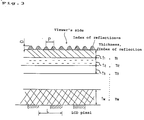
- Equations (1) and (2) as shown in Fig. 3, the period of lattice of the diffraction grating is represented by P, the period of the pixels of the image display device is represented by L, the stepwise difference between the recessed portion and the projected portion in the lattice portion of the diffraction grating is represented by D, the index of the refraction of the lattice portion of the diffraction grating is represented by n, a number of layers of from faces of the pixels of the image display device on the viewer's side to the base portion of the diffraction grating is represented by M, the index of refraction of each of the layers of from the faces of the pixels of the image display device on the viewer's side to the base portion of the diffraction grating is represented by ni and a thickness of each of the layers is represented by ti, respectively. Further, the index of refraction of air is determined to be 1.
- Equation (3) L/10 ⁇ T ⁇ D ⁇ (n-1)/P ⁇ 3 ⁇ L
- Fig. 4 shows the outline structure of a second embodiment of an image display apparatus according to the present invention.
- a liquid crystal panel 7 of a TFT type is used as an image display device and a lattice portion 4 of a diffraction grating is provided directly on a polarizing plate 6 that is disposed on the side opposed the side of a light source 5.
- the poly(vinyl alcohol) film is sandwiched by the TAC films in the polarizing plate 6. That is, the TAC film on the viewer's side of the polarizing plate corresponds to the base portion of the diffraction grating.
- a hard coating layer 8 and an antireflection film 9 are installed from the side of the lattice portion 4 of the diffraction grating, on the viewer's side of the diffraction grating. According to this embodiment of the image display apparatus an apparatus in which the brightness of displayed image is high and the displayed image is difficult to be flawed, is provided.
- this image display apparatus there are arranged four layers of a glass substrate, (which is one of constituent elements of the liquid crystal panel, not illustrated), the TAC film, the poly(vinyl alcohol) film and the TAC film (the base portion of the diffraction grating) from the faces of the pixels of the image display device on the viewer's side to the base portion of the diffraction grating if the adhesive layers adhering the TAC films to the poly(vinyl alcohol) film, are neglected in calculation.
- the viewing angle is enlarged and excellent image with insignificant deterioration of image quality is obtained.
Landscapes
- Physics & Mathematics (AREA)
- Nonlinear Science (AREA)
- Mathematical Physics (AREA)
- Chemical & Material Sciences (AREA)
- Crystallography & Structural Chemistry (AREA)
- General Physics & Mathematics (AREA)
- Optics & Photonics (AREA)
- Liquid Crystal (AREA)
- Diffracting Gratings Or Hologram Optical Elements (AREA)
Abstract
Description
- The present invention relates to an image display apparatus using an image display device represented by liquid crystal panels.
- An image display apparatus using an image display device in which pixels are arranged in a dot-like form and which is represented by a light emitting diode array, a liquid crystal panel of a TFT (thin film transistor) active matrix type etc., has been developed. According to such an image display apparatus the contrast of an image displayed on the image display apparatus is significantly changed by the magnitude of an angle made by a direction for viewing the image display apparatus and a direction orthogonal to a display face of the image display apparatus (that is, an angle whereby a direction in which a viewer is disposed, in view from the display face of the image display apparatus, is deviated from a direction orthogonal to a frontal face of the image display apparatus) and fair image quality can be provided only when the viewer views the image display apparatus right in front thereof or substantially right in front thereof. That is, a viewing angle providing fair image quality is narrow in such an image display apparatus. Accordingly, it is difficult for a number of persons to view one display face of the image display apparatus at the same time. Further, when a large screen of the image display apparatus is viewed in close proximity, there is recognized the difference of contrast between the central portion and the peripheral portion of the display face whereby the image quality is deteriorated.
- The above-mentioned problem is particularly significant in an image display apparatus using a liquid crystal panel as an image display device. In order to resolve such a problem a liquid crystal display apparatus (refer to Japanese Unexamined Patent Publication No. 65175/1981) in which a polyhedron lens is arranged on the viewer's side of a liquid crystal panel, a display apparatus (refer to Japanese Unexamined Patent Publication No. 25399/1978) in which a concave lens array is arranged, and the like have been developed. However, sufficient image quality has not been achieved in these conventional image display devices although the viewing angles can be enlarged.
- To resolve the above-mentioned problem, it is an object of the present invention to provide an image display apparatus capable of enlarging the viewing angle without deteriorating the image quality.
- According to a first aspect of the present invention resolving the above-mentioned problem, an image display apparatus includes an image display device in which pixels are arranged in a dot-like form and a diffraction grating having a lattice face, wherein the diffraction grating is arranged on a display optical path of the image display device such that the lattice face of the diffraction grating faces toward a side of a viewer and the viewing angle of the image display device is enlarged by the diffraction grating. Further, according to a second aspect of the present invention resolving the above-mentioned problem, an image display apparatus includes an image display device having a display face on which a diffraction grating having a lattice face is provided such that the lattice face thereof faces toward a side of a viewer, wherein the viewing angle of the image display device is enlarged by the diffraction grating.
- According to the image display apparatus in accordance with the first or the second aspect of the present invention, it is preferable for obtaining higher image quality to satisfy the following equation (1)


- According to the present invention, light emitted from the pixels of the image display device is diffracted, bent and diffused by the diffraction grating provided on the display optical path of the image display device or at the display face of the image display device and therefore, the extent of emitting light is expanded. In this way the viewing angle of the image display apparatus is enlarged.
- There are CRT, light emitting diode, liquid crystal panel etc. as the image display devices that are used in the present invention. As systems of a liquid crystal panel, there are the simple matrix drive system, the active matrix drive system etc. and as modes of liquid crystal, there are twist nematic type, super twist nematic type etc. as representative ones.
- The diffraction grating according to the present invention is manufactured by, for example, the following process. A transparent film or a transparent plate made of polycarbonate, acrylic resin, TAC etc. is mounted at a mold (or stamper) on which a recess and projection pattern corresponding to the lattice of the diffraction grating is provided, the transparent film etc. is thermally deformed in the mold (or on the stamper), the thermally deformed transparent film etc. is cooled and thereafter, the mold or the stamper is removed. The diffraction grating according to the present invention is manufactured also by the following process. An ultraviolet ray setting transparent resin is coated on a transparent film or a transparent plate and an ultraviolet ray is irradiated on the transparent film or the transparent plate while a mold (or a stamper) on which a recess and projection pattern corresponding to the lattice of the diffraction grating is provided, is being mounted on a face thereof coated with the ultraviolet ray setting transparent resin whereby the transparent resin is cured. A thermosetting transparent resin may be coated thereon in place of the ultraviolet ray setting transparent resin and the transparent resin may be thermally cured. Further, the diffraction grating according to the present invention can also be manufactured by coating an ultraviolet ray setting transparent resin on a transparent film or a transparent plate, irradiating an ultraviolet ray on the transparent resin through a photomask on which a recess and projection pattern corresponding to the lattice of the diffraction grating is printed and thereafter, developing the ultraviolet ray setting transparent resin. Furthermore, the diffraction grating according to the present invention can be manufactured by performing an injection molding by using a thermoplastic transparent resin made of polycarbonate, acrylic resin etc.
- The side of a plane face (face on the side where the lattice is not formed) of the diffraction grating in the present invention is disposed on the side of the pixels of the image display device and this face can be pasted together with a protective plate of the image display device. Thereby, an air layer between the image display device and the diffraction grating is dispensed with, reflection of light caused at an interface between the image display device and air and at an interface between the diffraction grating and air can be suppressed and a ratio of light emitted from the image display device to the outside via the diffraction grating can be increased. Also, a similar effect can be provided by forming the diffraction grating directly on the protective plate of the liquid crystal panel or the polarizing plate of the liquid crystal panel.
- Although high brightness is generally required in an image display apparatus, when the diffraction grating is installed in front of the image display device (the display optical path of the image display device or the display face of the image display device), the brightness of the image display apparatus may be lowered due to an increase in a number of faces reflecting light from the image display device such as the interface between the diffraction grating and air. This problem can be resolved by pasting together the diffraction grating and the protective plate etc. When a further higher brightness is necessary, an anti-reflection film may be coated on the viewer's side (face having the lattice) of the diffraction grating. Incidentally, it is preferable for obtaining the high brightness that the light ray transmittance of the diffraction grating is 97% or more in a wavelength range of 450 through 650 nm.
- It is more preferable for obtaining the high contrast to use a diffraction grating having a sectional shape in a continuous curve than in the case where a diffraction grating having a discontinuous sectional shape (for example, rectangular shape) is used. It is preferable that the period of the diffraction grating is smaller than the period of the pixels of the image display device since the pattern of lattice in the diffraction grating is not observed. It is preferable that the depth of lattice (a stepwise difference between a recessed portion and a projected portion) of the diffraction grating is 1 µm or more since the diffraction efficiency of the diffraction grating is improved.
- Image quality of a small-sized television receiver etc. is deteriorated during its use due to contamination of a screen. This problem can be solved by coating a contamination preventive coating on the lattice face of the diffraction grating by using a fluorine group resin etc. An excellent contamination preventive function can be provided by rendering the angle of contact of water at the surface of the diffraction grating 70° or more by performing the contamination preventive coating.
- The image quality is deteriorated also by making a flaw on the screen while using thereof. It is preferable that a hard coating agent is coated on the lattice face (viewer's side) of the diffraction grating and the pencil hardness of this face is enhanced to H or higher.
- Incidentally, when a flourescent lamp etc. is reflected by the screen, the contrast is deteriorated and also the recognizability is deteriorated since the reflected image overlaps the original image in the screen. This problem can be resolved by subjecting the recess and projection face of the diffraction grating to a nonglaring treatment without deteriorating the image.
- Fig. 1 is an outline structural view showing a first embodiment of an image display apparatus according to the present invention;
- Fig. 2 is an outline structural view showing an image display apparatus used for evaluation;
- Fig. 3 is a view schematically showing a section of a first embodiment of the image display apparatus according to the present invention; and
- Fig. 4 is an outline structural view showing a second embodiment of an image display apparatus according to the present invention.
- Fig. 1 illustrates the outline structure of a first embodiment of an image display apparatus according to the present invention. The image display apparatus is provided with an
image display device 2 in whichpixels 1 are arranged in a dot-like form and a diffraction grating 4 having a lattice face. The diffraction grating 4 is arranged on a display optical path of theimage display device 2 such that the lattice face of the diffraction grating 4 faces toward a viewer'sside 3. Thepixels 1 of the image display device control light emitted by the pixels per se, light incident on the pixels from a light source provided on the side opposed to the viewer's side or light incident on the pixels from a light source provided on the viewer's side and theimage display device 2 displays an image by controlling the pixels. The diffraction grating in the image display apparatus as illustrated in Fig. 1, is provided with a sectional shape in a continuous curve and the sectional shape is substantially in a form of sine wave as shown by Fig. 1. - By arranging the diffraction grating on the display optical path of the image display device as in the above-mentioned image display apparatus, light emitted from the pixels of the image display device is diffracted, bent and diffused by the diffraction grating provided on the display optical path of the image display device or on the display face of the image display device and the viewing angle of the image display apparatus is enlarged. However, on the other hand deterioration of image quality due to whitening of image may be caused. The degree of the deterioration of image quality is varied depending on the position for installing the diffraction grating, the period of the diffraction grating, the depth of lattice of the diffraction grating etc. Now, assume the case where the diffraction grating is arranged on the viewer's side of a liquid crystal panel, as an example. A portion of the apparatus from the pixels of the liquid crystal panel to the diffraction grating is in a multi-layered structure of a glass substrate protecting the pixels of the liquid crystal panel, a TAC film of a polarizing plate, a poly(vinyl alcohol) film of the polarizing plate, an adhesive layer adhering the TAC film to the poly(vinyl alcohol) film, an air layer etc. and thicknesses and the indexes of refraction of these respective layers pose a significant influence on the image quality. Hence, the image was evaluated by using samples of various diffraction gratings prepared by varying the depth of lattice and the period of the diffraction grating.
- Now, the outline structure of the image display apparatus that was used for the evaluation is shown in Fig. 2. In this image display apparatus light emitted from a
light source 5 is incident on aliquid crystal panel 7 of a TFT (thin film transistor) type in which polarizingplates 6 each sandwiching the poly(vinyl alcohol) film by the TAC films, are arranged on the top and the bottom faces thereof, where a control is performed to allow light to transmit through or block light by the pixels of theliquid crystal panel 7 whereby the image is displayed. Adiffraction grating 4 is arranged on the viewer'sside 3 which is opposed to the side of thelight source 5 and light transmitted through the pixels is diffracted and the viewing angle is enlarged by the diffraction grating as shown by Fig. 2. In this image display apparatus five layers of a glass substrate (which is one of constituent elements of the liquid crystal panel, not illustrated), the TAC film, the poly(vinyl alcohol) film, the TAC film and the air layer, are arranged from the faces of the pixels of the image display device on the viewer's side to the base portion of the diffraction grating. The diffraction gratings were prepared by varying the period of lattice of the diffraction grating to 50µm or 100µm. The diffraction gratings were prepared by varying the stepwise difference between the recessed portion and the projected portion (namely, the thickness of the lattice portion of the diffraction grating) in the recess and projection of the diffraction grating in a range of 1.4 through 294 µm. Further, the index of refraction at the portion of the diffraction grating was determined to be 1.53. The result of evaluation of image quality is shown by Table 1. Incidentally, the thickness of each of the adhesive layers respectively adhering the TAC film to the poly(vinyl alcohol) film was extremely small and therefore, it was neglected in calculation.Table 1 Value of α Result of evaluation of image quality Result of evaluation of viewing angle enlargement 0.05 o x 0.1 o △ 0.2 o △ 0.5 o o 1.0 o o 2.0 o o 2.5 △ o 3.0 △ o 3.5 △ o 4.0 △ o 4.5 x o - α in Table is a value given by the following equation.

- With regard to the result of evaluation of image quality, o indicates no deterioration of image quality, △ indicates inconsiderable deterioration of image quality and x indicates considerable deterioration of image quality, respectively. With regard to the result of evaluation of viewing angle enlargement, o indicates significant viewing angle enlarging feature, △ indicates insignificant viewing angle enlarging feature and x indicates no viewing angle enlarging feature, respectively.
- It was found from these results that the viewing angle was enlarged while high image quality was being maintained when the following Equation (1) was satisfied.


- In Equations (1) and (2), as shown in Fig. 3, the period of lattice of the diffraction grating is represented by P, the period of the pixels of the image display device is represented by L, the stepwise difference between the recessed portion and the projected portion in the lattice portion of the diffraction grating is represented by D, the index of the refraction of the lattice portion of the diffraction grating is represented by n, a number of layers of from faces of the pixels of the image display device on the viewer's side to the base portion of the diffraction grating is represented by M, the index of refraction of each of the layers of from the faces of the pixels of the image display device on the viewer's side to the base portion of the diffraction grating is represented by ni and a thickness of each of the layers is represented by ti, respectively. Further, the index of refraction of air is determined to be 1.
- According to the present invention, it is preferable in view of providing higher image quality to satisfy the following Equation (3) in place of Equation (1).

- Further higher image quality can be provided by using a diffraction grating satisfying the following Equation (4).

- Fig. 4 shows the outline structure of a second embodiment of an image display apparatus according to the present invention. According to the image display apparatus a
liquid crystal panel 7 of a TFT type is used as an image display device and alattice portion 4 of a diffraction grating is provided directly on apolarizing plate 6 that is disposed on the side opposed the side of alight source 5. The poly(vinyl alcohol) film is sandwiched by the TAC films in thepolarizing plate 6. That is, the TAC film on the viewer's side of the polarizing plate corresponds to the base portion of the diffraction grating. A hard coating layer 8 and anantireflection film 9 are installed from the side of thelattice portion 4 of the diffraction grating, on the viewer's side of the diffraction grating. According to this embodiment of the image display apparatus an apparatus in which the brightness of displayed image is high and the displayed image is difficult to be flawed, is provided. In this image display apparatus there are arranged four layers of a glass substrate, (which is one of constituent elements of the liquid crystal panel, not illustrated), the TAC film, the poly(vinyl alcohol) film and the TAC film (the base portion of the diffraction grating) from the faces of the pixels of the image display device on the viewer's side to the base portion of the diffraction grating if the adhesive layers adhering the TAC films to the poly(vinyl alcohol) film, are neglected in calculation. - According to the image display device of the present invention the viewing angle is enlarged and excellent image with insignificant deterioration of image quality is obtained.
Claims (12)
- An image display apparatus comprising:an image display device in which pixels are arranged in a dot-like form;a diffraction grating having a lattice face; andwherein the diffraction grating is arranged on a display optical path of the image display device such that the lattice face of the diffraction grating faces toward a side of a viewer and a viewing angle of the image display device is enlarged by the diffraction grating.
- An image display apparatus including an image display device having a display face on which a diffraction grating having a lattice face is provided such that the lattice face of the diffraction grating faces toward a side of a viewer, wherein a viewing angle of the image display device is enlarged by the diffraction grating.
- The image display apparatus according to any one of claim 1 through claim 2, wherein the image display device is a liquid crystal panel.
- The image display apparatus according to claim 3, wherein the liquid crystal panel includes a protective plate and the diffraction grating is formed on the protective plate.
- The image display apparatus according to claim 3, wherein the liquid crystal panel includes a polarizing plate and the diffraction grating is formed on the polarizing plate.
- The image display apparatus according to any one of claim 1 through claim 5 which satisfies the following Equation (1):


- The image display apparatus according to any one of claim 1 through claim 6, wherein a light ray transmittance of the diffraction grating in a range of a wavelength of 450 through 650 nm is 97% or more.
- The image display apparatus according to any one of claim 1 through claim 7, wherein the diffraction grating is provided with a sectional shape in a continuous curve.
- The image display apparatus according to any one of claim 1 through claim 8,wherein the period of the lattice of the diffraction grating is smaller than the period of the pixels of the image display device.
- The image display apparatus according to any one of claim 1 through claim 9, wherein the stepwise difference between the recessed portion and the projected portion of the lattice in the diffraction grating is 1 µm or more.
- The image display apparatus according to any one of claim 1 through claim 10, wherein the angle of contact of water at the lattice face in the diffraction grating is 70° or more.
- The image display apparatus according to any one of claim 1 through claim 11, wherein the pencil hardness of the lattice face in the diffraction grating is H or higher.
Applications Claiming Priority (3)
| Application Number | Priority Date | Filing Date | Title |
|---|---|---|---|
| JP216992/95 | 1995-08-25 | ||
| JP21699295 | 1995-08-25 | ||
| JP21699295 | 1995-08-25 |
Publications (3)
| Publication Number | Publication Date |
|---|---|
| EP0760490A2 true EP0760490A2 (en) | 1997-03-05 |
| EP0760490A3 EP0760490A3 (en) | 1997-11-12 |
| EP0760490B1 EP0760490B1 (en) | 2001-05-16 |
Family
ID=16697120
Family Applications (1)
| Application Number | Title | Priority Date | Filing Date |
|---|---|---|---|
| EP96113535A Expired - Lifetime EP0760490B1 (en) | 1995-08-25 | 1996-08-23 | Image display apparatus |
Country Status (5)
| Country | Link |
|---|---|
| US (1) | US6067137A (en) |
| EP (1) | EP0760490B1 (en) |
| KR (1) | KR100210992B1 (en) |
| DE (1) | DE69612800D1 (en) |
| TW (1) | TW469359B (en) |
Cited By (10)
| Publication number | Priority date | Publication date | Assignee | Title |
|---|---|---|---|---|
| US7114820B1 (en) | 1998-12-30 | 2006-10-03 | Nokia Mobile Phones, Ltd. | Backlighting light pipe for illuminating a flat-panel display |
| EP2746894A3 (en) * | 2012-12-19 | 2017-05-17 | Nokia Technologies Oy | Flexible apparatus structure |
| CN109031502A (en) * | 2018-09-30 | 2018-12-18 | 惠科股份有限公司 | polarizing structure and display device |
| CN109100825A (en) * | 2018-09-30 | 2018-12-28 | 惠科股份有限公司 | Polarizer and display device |
| CN109143676A (en) * | 2018-09-30 | 2019-01-04 | 惠科股份有限公司 | polarizing structure and display device |
| CN109143674A (en) * | 2018-09-30 | 2019-01-04 | 惠科股份有限公司 | polarizing structure and display device |
| CN109188591A (en) * | 2018-09-30 | 2019-01-11 | 惠科股份有限公司 | Polarizer and display device |
| CN109188592A (en) * | 2018-09-30 | 2019-01-11 | 惠科股份有限公司 | polarizing structure and display device |
| USRE47725E1 (en) | 2011-03-31 | 2019-11-12 | Cheng Mei Materials Technology Corporation | Display apparatus and liquid crystal display device |
| EP2506068B1 (en) * | 2011-03-31 | 2019-11-27 | Cheng Mei Materials Technology Corporation | Liquid crystal display apparatus with a diffractive optical element |
Families Citing this family (25)
| Publication number | Priority date | Publication date | Assignee | Title |
|---|---|---|---|---|
| JPH09281508A (en) * | 1996-04-12 | 1997-10-31 | Semiconductor Energy Lab Co Ltd | Liquid crystal display device and its manufacture |
| JP3938253B2 (en) | 1997-12-26 | 2007-06-27 | 日本板硝子株式会社 | Resin erecting equal-magnification lens array and manufacturing method thereof |
| JP3710368B2 (en) * | 2000-09-25 | 2005-10-26 | シャープ株式会社 | Manufacturing method of laminated film |
| AU2002224242B2 (en) * | 2000-11-17 | 2007-05-17 | Pure Depth Limited | Altering surface of display screen from matt to optically smooth |
| NZ511255A (en) * | 2001-04-20 | 2003-12-19 | Deep Video Imaging Ltd | Multi-focal plane display having an optical retarder and a diffuser interposed between its screens |
| US20030035231A1 (en) * | 2001-08-03 | 2003-02-20 | Epstein Kenneth A. | Optical film having microreplicated structures; and methods |
| NZ514119A (en) * | 2001-09-11 | 2004-06-25 | Deep Video Imaging Ltd | Improvement to instrumentation |
| NZ514500A (en) * | 2001-10-11 | 2004-06-25 | Deep Video Imaging Ltd | A multiplane visual display unit with a transparent emissive layer disposed between two display planes |
| US6831786B2 (en) * | 2002-03-11 | 2004-12-14 | Eastman Kodak Company | Surface formed complex multi-layered polymer lenses for light diffusion |
| US7742239B2 (en) * | 2002-03-17 | 2010-06-22 | Puredepth Limited | Method to control point spread function of an image |
| CN100394252C (en) * | 2002-07-15 | 2008-06-11 | 普尔·代普斯有限公司 | Improved multi-layer display |
| NZ521505A (en) * | 2002-09-20 | 2005-05-27 | Deep Video Imaging Ltd | Multi-view display |
| NZ526028A (en) * | 2003-05-21 | 2006-02-24 | Pure Depth Ltd | Backlighting system for display screen utilised to control the distribution of power to at least one light source |
| US20060152817A1 (en) * | 2005-01-12 | 2006-07-13 | Goro Noto | Optical device |
| CN101897196A (en) * | 2007-08-22 | 2010-11-24 | 普尔·代普斯有限公司 | Determining the position of an interstitial diffuser for a multi-component display |
| TWI509330B (en) * | 2010-08-05 | 2015-11-21 | Chi Mei Materials Technology Corp | Display device |
| CN105629563B (en) * | 2011-01-21 | 2019-01-18 | 群创光电股份有限公司 | Backlight module and liquid crystal display device |
| JP6251472B2 (en) * | 2011-08-11 | 2017-12-20 | チ メイ マテリアルズ テクノロジー コーポレーション | Display device and polarizer for multi-domain vertical alignment liquid crystal display device |
| US8733958B2 (en) * | 2011-11-18 | 2014-05-27 | Shenzhen China Star Optoelectronics Technology Co., Ltd. | Flat panel display device and stereoscopic display device |
| KR102260184B1 (en) * | 2014-02-26 | 2021-06-04 | 삼성디스플레이 주식회사 | Cover window and display device having the same |
| US10564322B2 (en) * | 2017-04-27 | 2020-02-18 | Pure Depth Limited | Diffractive antiglare in a multi-layered display |
| TWI649586B (en) * | 2017-07-20 | 2019-02-01 | Benq Materials Corporation | Light weight guiding film and manufacturing method thereof |
| TWI633378B (en) * | 2017-12-14 | 2018-08-21 | 明基材料股份有限公司 | Optical film |
| CN109958380B (en) * | 2017-12-26 | 2021-04-02 | 清华大学 | Hydrophobic windows and houses and cars using the same |
| CN111564119B (en) * | 2020-05-12 | 2023-03-28 | Oppo广东移动通信有限公司 | Display screen assembly, manufacturing method thereof and electronic device |
Family Cites Families (12)
| Publication number | Priority date | Publication date | Assignee | Title |
|---|---|---|---|---|
| US3809457A (en) * | 1972-10-13 | 1974-05-07 | Eastman Kodak Co | Radiation-redistributive devices |
| US4184746A (en) * | 1972-11-06 | 1980-01-22 | Coale Edgar B | Transmissive diffractive phase-grating |
| US4984872A (en) * | 1989-06-16 | 1991-01-15 | Rockwell International Corporation | Wide viewing angle avionics liquid crystal display |
| EP0479490A3 (en) * | 1990-10-02 | 1992-08-12 | Physical Optics Corporation | Volume holographic diffuser |
| JPH05134252A (en) * | 1991-11-12 | 1993-05-28 | Nitto Denko Corp | Liquid crystal display device, planar point light source and planar parallel light source |
| JPH05232460A (en) * | 1992-02-20 | 1993-09-10 | Kuraray Co Ltd | Transmission type liquid crystal display element |
| US5528720A (en) * | 1992-03-23 | 1996-06-18 | Minnesota Mining And Manufacturing Co. | Tapered multilayer luminaire devices |
| KR0120397B1 (en) * | 1992-04-28 | 1997-10-22 | 나카무라 히사오 | Image display apparatus |
| JP3204471B2 (en) * | 1992-11-06 | 2001-09-04 | 株式会社クラレ | Optical low-pass filter and imaging device |
| JPH07114015A (en) * | 1993-10-19 | 1995-05-02 | Olympus Optical Co Ltd | Liquid crystal display device |
| JPH07218901A (en) * | 1994-01-28 | 1995-08-18 | Kuraray Co Ltd | Liquid crystal display |
| US5629784A (en) * | 1994-04-12 | 1997-05-13 | Ois Optical Imaging Systems, Inc. | Liquid crystal display with holographic diffuser and prism sheet on viewer side |
-
1996
- 1996-08-14 US US08/696,793 patent/US6067137A/en not_active Expired - Fee Related
- 1996-08-23 DE DE69612800T patent/DE69612800D1/en not_active Expired - Lifetime
- 1996-08-23 EP EP96113535A patent/EP0760490B1/en not_active Expired - Lifetime
- 1996-08-23 KR KR1019960034954A patent/KR100210992B1/en not_active Expired - Fee Related
- 1996-08-24 TW TW085110337A patent/TW469359B/en not_active IP Right Cessation
Cited By (14)
| Publication number | Priority date | Publication date | Assignee | Title |
|---|---|---|---|---|
| US7114820B1 (en) | 1998-12-30 | 2006-10-03 | Nokia Mobile Phones, Ltd. | Backlighting light pipe for illuminating a flat-panel display |
| US7192175B2 (en) | 1998-12-30 | 2007-03-20 | Nokia Mobile Phones, Ltd. | Backlighting light pipe for illuminating a flat-panel display |
| US7712942B2 (en) | 1998-12-30 | 2010-05-11 | Nokia Corporation | Backlighting light pipe for illuminating a flat-panel display |
| EP2506068B1 (en) * | 2011-03-31 | 2019-11-27 | Cheng Mei Materials Technology Corporation | Liquid crystal display apparatus with a diffractive optical element |
| USRE47725E1 (en) | 2011-03-31 | 2019-11-12 | Cheng Mei Materials Technology Corporation | Display apparatus and liquid crystal display device |
| EP2746894A3 (en) * | 2012-12-19 | 2017-05-17 | Nokia Technologies Oy | Flexible apparatus structure |
| CN109143676A (en) * | 2018-09-30 | 2019-01-04 | 惠科股份有限公司 | polarizing structure and display device |
| CN109143674A (en) * | 2018-09-30 | 2019-01-04 | 惠科股份有限公司 | polarizing structure and display device |
| CN109188591A (en) * | 2018-09-30 | 2019-01-11 | 惠科股份有限公司 | Polarizer and display device |
| CN109188592A (en) * | 2018-09-30 | 2019-01-11 | 惠科股份有限公司 | polarizing structure and display device |
| CN109100825A (en) * | 2018-09-30 | 2018-12-28 | 惠科股份有限公司 | Polarizer and display device |
| CN109031502A (en) * | 2018-09-30 | 2018-12-18 | 惠科股份有限公司 | polarizing structure and display device |
| WO2020062563A1 (en) * | 2018-09-30 | 2020-04-02 | 惠科股份有限公司 | Polarizer structure and display device |
| WO2020062560A1 (en) * | 2018-09-30 | 2020-04-02 | 惠科股份有限公司 | Polarizing structure and display device |
Also Published As
| Publication number | Publication date |
|---|---|
| EP0760490B1 (en) | 2001-05-16 |
| US6067137A (en) | 2000-05-23 |
| EP0760490A3 (en) | 1997-11-12 |
| KR100210992B1 (en) | 1999-07-15 |
| DE69612800D1 (en) | 2001-06-21 |
| TW469359B (en) | 2001-12-21 |
| KR970011952A (en) | 1997-03-29 |
Similar Documents
| Publication | Publication Date | Title |
|---|---|---|
| US6067137A (en) | Image display apparatus with hydrophobic diffraction grating for an enlarged viewing angle | |
| US7821717B2 (en) | Lenticular lens array element | |
| US6822707B2 (en) | Optical sheet and display device having the optical sheet | |
| US20170343826A1 (en) | Optical arrangement and an autostereoscopic display device incorporating the same | |
| EP0729597B1 (en) | Backlight assembly for an electro-optical display | |
| KR100993232B1 (en) | Method for manufacturing optical element, optical element, illumination optical device, display device and electronic device | |
| US5555476A (en) | Microlens array sheet for a liquid crystal display, method for attaching the same and liquid crystal display equipped with the same | |
| US6942959B2 (en) | Display screen and method of manufacture therefor | |
| US5661531A (en) | Tiled, flat-panel display having invisible seams | |
| EP0840183B1 (en) | Holography device | |
| EP0750209A1 (en) | Light guiding sheet and manufacturing method thereof | |
| EP1484639A1 (en) | Projection screen and manufacturing method thereof | |
| CA2458380A1 (en) | Prismatic optical display | |
| JPH09127309A (en) | Microlens array sheet and liquid crystal display using the same | |
| EP1998573A2 (en) | Stereoscopic display and phase different plate | |
| JPH07120743A (en) | How to attach the microlens array sheet | |
| JPH0949925A (en) | Field-of-view film and liquid crystal display using the same | |
| US7421180B2 (en) | Light guide apparatus for use in rear projection display environments | |
| KR100932606B1 (en) | Optical film and backlight unit including same | |
| CN100541322C (en) | Rear projection type screen and rear projection type image display apparatus | |
| JPH07104271A (en) | Liquid crystal display | |
| JPH0743501A (en) | Microlens array sheet and liquid crystal display using the same | |
| JPH09127878A (en) | Image display device | |
| JPH07218901A (en) | Liquid crystal display | |
| JP2022035209A (en) | Screen and video display device |
Legal Events
| Date | Code | Title | Description |
|---|---|---|---|
| PUAI | Public reference made under article 153(3) epc to a published international application that has entered the european phase |
Free format text: ORIGINAL CODE: 0009012 |
|
| AK | Designated contracting states |
Kind code of ref document: A2 Designated state(s): DE FR GB NL |
|
| PUAL | Search report despatched |
Free format text: ORIGINAL CODE: 0009013 |
|
| AK | Designated contracting states |
Kind code of ref document: A3 Designated state(s): DE FR GB NL |
|
| 17P | Request for examination filed |
Effective date: 19980213 |
|
| 17Q | First examination report despatched |
Effective date: 19990222 |
|
| GRAG | Despatch of communication of intention to grant |
Free format text: ORIGINAL CODE: EPIDOS AGRA |
|
| 17Q | First examination report despatched |
Effective date: 19990222 |
|
| GRAG | Despatch of communication of intention to grant |
Free format text: ORIGINAL CODE: EPIDOS AGRA |
|
| GRAG | Despatch of communication of intention to grant |
Free format text: ORIGINAL CODE: EPIDOS AGRA |
|
| GRAH | Despatch of communication of intention to grant a patent |
Free format text: ORIGINAL CODE: EPIDOS IGRA |
|
| GRAH | Despatch of communication of intention to grant a patent |
Free format text: ORIGINAL CODE: EPIDOS IGRA |
|
| GRAA | (expected) grant |
Free format text: ORIGINAL CODE: 0009210 |
|
| AK | Designated contracting states |
Kind code of ref document: B1 Designated state(s): DE FR GB NL |
|
| REF | Corresponds to: |
Ref document number: 69612800 Country of ref document: DE Date of ref document: 20010621 |
|
| PG25 | Lapsed in a contracting state [announced via postgrant information from national office to epo] |
Ref country code: DE Free format text: LAPSE BECAUSE OF FAILURE TO SUBMIT A TRANSLATION OF THE DESCRIPTION OR TO PAY THE FEE WITHIN THE PRESCRIBED TIME-LIMIT Effective date: 20010817 |
|
| PG25 | Lapsed in a contracting state [announced via postgrant information from national office to epo] |
Ref country code: GB Free format text: LAPSE BECAUSE OF NON-PAYMENT OF DUE FEES Effective date: 20010823 |
|
| ET | Fr: translation filed | ||
| PLBE | No opposition filed within time limit |
Free format text: ORIGINAL CODE: 0009261 |
|
| STAA | Information on the status of an ep patent application or granted ep patent |
Free format text: STATUS: NO OPPOSITION FILED WITHIN TIME LIMIT |
|
| GBPC | Gb: european patent ceased through non-payment of renewal fee |
Effective date: 20010823 |
|
| 26N | No opposition filed | ||
| PGFP | Annual fee paid to national office [announced via postgrant information from national office to epo] |
Ref country code: FR Payment date: 20090814 Year of fee payment: 14 |
|
| PGFP | Annual fee paid to national office [announced via postgrant information from national office to epo] |
Ref country code: NL Payment date: 20090803 Year of fee payment: 14 |
|
| REG | Reference to a national code |
Ref country code: NL Ref legal event code: V1 Effective date: 20110301 |
|
| REG | Reference to a national code |
Ref country code: FR Ref legal event code: ST Effective date: 20110502 |
|
| PG25 | Lapsed in a contracting state [announced via postgrant information from national office to epo] |
Ref country code: NL Free format text: LAPSE BECAUSE OF NON-PAYMENT OF DUE FEES Effective date: 20110301 |
|
| PG25 | Lapsed in a contracting state [announced via postgrant information from national office to epo] |
Ref country code: FR Free format text: LAPSE BECAUSE OF NON-PAYMENT OF DUE FEES Effective date: 20100831 |