EP0755149B1 - Method and system for digitizing ccd data - Google Patents
Method and system for digitizing ccd data Download PDFInfo
- Publication number
- EP0755149B1 EP0755149B1 EP95201987A EP95201987A EP0755149B1 EP 0755149 B1 EP0755149 B1 EP 0755149B1 EP 95201987 A EP95201987 A EP 95201987A EP 95201987 A EP95201987 A EP 95201987A EP 0755149 B1 EP0755149 B1 EP 0755149B1
- Authority
- EP
- European Patent Office
- Prior art keywords
- ccd
- clock signal
- analog
- data
- converter
- Prior art date
- Legal status (The legal status is an assumption and is not a legal conclusion. Google has not performed a legal analysis and makes no representation as to the accuracy of the status listed.)
- Expired - Lifetime
Links
- 238000000034 method Methods 0.000 title claims description 8
- 238000001208 nuclear magnetic resonance pulse sequence Methods 0.000 claims description 4
- 238000010586 diagram Methods 0.000 description 6
- 230000003750 conditioning effect Effects 0.000 description 5
- 239000000872 buffer Substances 0.000 description 4
- 230000003111 delayed effect Effects 0.000 description 4
- 239000003990 capacitor Substances 0.000 description 2
- 238000010276 construction Methods 0.000 description 2
- 230000001419 dependent effect Effects 0.000 description 2
- 230000001360 synchronised effect Effects 0.000 description 2
- 238000006243 chemical reaction Methods 0.000 description 1
- 239000000470 constituent Substances 0.000 description 1
- 230000001934 delay Effects 0.000 description 1
- 238000002347 injection Methods 0.000 description 1
- 239000007924 injection Substances 0.000 description 1
- 230000010354 integration Effects 0.000 description 1
- 238000012986 modification Methods 0.000 description 1
- 230000004048 modification Effects 0.000 description 1
- 238000007493 shaping process Methods 0.000 description 1
- 230000007704 transition Effects 0.000 description 1
Images



Classifications
-
- H—ELECTRICITY
- H04—ELECTRIC COMMUNICATION TECHNIQUE
- H04N—PICTORIAL COMMUNICATION, e.g. TELEVISION
- H04N5/00—Details of television systems
- H04N5/14—Picture signal circuitry for video frequency region
Definitions
- the invention relates to a method and a system for digitizing analog data. More particularly, the invention relates to a method and system for digitizing data that have been generated by an image sensor including a charge coupled device (ccd), a MOS-imager which is also known as a "charge injection device", and the like.
- a charge coupled device ccd
- MOS-imager which is also known as a "charge injection device”, and the like.
- Charge coupled devices usually comprise a large number of light sensitive cells which generate and hold electric charges in response to light incident thereupon. The charges accumulated in each cell during a certain integration time are then transferred to one or more outputs of the ccd and are converted into electric voltages under the control of and in synchronism with a clock signal.
- the analog data obtained in this way at the output of the ccd are supplied to an A/D-converter (ADC) via a conditioning circuit in which the offset and the gain factor are adapted to the input characteristics of the ADC.
- ADC A/D-converter
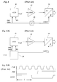
- a block diagram of a conventional ccd system of this type is illustrated in Fig. 3A.
- a ccd-array 10 supplies CCD-data V ccd to the conditioning circuit 12 the output of which is connected to the data input of ADC 14.
- the ccd-array is of a type which is controlled by a clock signal PHI, the inverted clock signal PHIn and a reset signal RS.
- the waveforms of the signals V ccd , PHI and RS are shown in Fig. 3B.
- the signals PHI and PHIn serve as transport clock pulses by which the charges accumulated in the ccd cells are shifted through analog shift registers to the output port of the ccd-array which operates as a charge/voltage converter.
- the signal RS provides reset pulses for this charge/voltage converter. When the converter has been reset in the "low" period of the signal RS, the output port assumes a voltage V os which corresponds to a ccd cell which has not been exposed to light.
- the next charge quantity is transferred to the output port and converted into a voltage V out which represents the amount of light that has been received by the corresponding ccd cell.
- This voltage V out has to be converted into digital data by the ADC 14.
- the ADC has to be controlled by an appropriate converter clock signal CONV in such a manner that the voltage of the signal V ccd is sampled and converted at a time t 0 within the period in which this signal is valid, i.e. has the value V out .
- the converter clock signal CONV is a pulse signal which is obtained by delaying the clock signal PHI by a predetermined delay time T.
- the voltage values are digitized at the H/L-transitions of the signal CONV.
- the converter clock signal CONV with the appropriate delay can be obtained in various ways, two of which are illustrated in Figs. 4 and 5.
- the signal CONV is derived from the clock signal PHI by means of a delay circuit 16.
- the delay circuit 16 may be formed for example by a series connection of a certain number of buffers each of which has a certain delay time, so that the total delay time is determined by the number of buffers.
- this implementation has the drawback that the delay times of commercially available buffers are known only within certain tolerances and the tolerances of the individual buffers in the series connection are accumulated, so that the total tolerance may become too large.
- a delay circuit may be used which is specifically designed for delaying a logic signal with a well defined delay time.
- delay circuits are comparatively expensive and may not be commercially available for the specific delay time which is needed in a given application. In such cases, a user specified device would have to be developed which would increase the costs even more.
- all the signals PHI, PHIn, RS and CONV are derived from a common basic clock signal CLK by means of a circuit 18 which is made up of a number of digital counters and may be considered as a state machine.
- the durations of the H and L periods of all signals output by the circuit 18 can only be integral multiples of the period of the basic clock signal CLK. Accordingly, in order to achieve a sufficient time resolution, the basic clock signal must have a comparatively high frequency which may be difficult to generate and may be unfavorable because it leads to the generation of electromagnetic noise and to problems of electromagnetic compatibility (EMC).
- EMC electromagnetic compatibility
- EP-A-0 755 194 which belongs to the prior art pursuant to Article 54(3) EPC discloses a method and system for digitizing analog data that have been generated as a pulse sequence in accordance with a clock signal and are supplied to an A/D-converter such that they will be sampled and digitised at appropriate timings, wherein the analog data are supplied to the A/D-converter via a correlator circuit for removing noise from the analog signal. Since the correlator circuit includes a low pass filter, it will also cause a certain delay in the analog signal. It is not disclosed in this document how the clock signal for the A/D-converter is obtained and how it is related to the clock signal for generating the analog data.
- the analog output signal of the data generating means is delayed in an analog delay circuit.
- An analog delay circuit that is suitable for this purpose can be made up of rather inexpensive components and permits to set the delay time with high accuracy and low tolerances, so that an efficient mass production of the ccd systems becomes possible.
- the analog delay circuit is rather insensitive to tolerances in the parameters of its constituents, such as inductance elements, capacitance elements and the like. It is admissible that the analog delay circuit distorts the waveform of the analog signal to some extent, as long as the portion of the output signal V ccd which represents the valid data V out remains unaffected for a time interval long enough for the ADC to sample the voltage value.
- the construction of the analog delay circuit may be simpler than that of a dedicated delay circuit for logic signals which is normally equipped with a pulse-shaping output stage.
- the delay time may be set as desired (steplessly) without any need for a high frequency basic clock signal.
- the highest clock frequency occurring in the system will be that of the clock signal PHI supplied to the ccd-array.
- a high frequency may be selected for the clock signal PHI in order to obtain a fast image sensor without causing EMC problems.
- the clock signal PHI (or the inverted clock signal PHIn or else the signal RS) can be used directly for controlling the ADC, thereby achieving a high robustness of the system as a whole, since the digital output signal obtained from the ADC will intrinsicly be synchronized with the system clock.
- the analog delay circuit may simply be formed by an all-pass filter or a low-pass filter, such as an LC-filter. Since the delay time of such a filter is dependent on its order (i.e., the number of complex impedance elements involved) and on its cut-off frequency (in case of a low-pass filter), the delay time can easily be adjusted by appropriately selecting the order and the cut-off frequency, respectively. In order to avoid a significant distortion of the analog signal, the filter should provide the same delay time for all frequency components passing therethrough.
- a low-pass filter has the additional advantage that undesirable high-frequency noise is filtered-out.
- the cut-off frequency should be significantly higher than the frequency of the clock signal PHI in order to make sure that the waveform of the output signal of the ccd-array is not distorted too much. It has been found that a Bessel filter, for example a fifth order Bessel filter, is particularly useful.
- the clock inputs of the ccd-array 10 and the ADC 14 are directly connected with each other and, accordingly, the converter clock signal CONV is identical with one of the clock signals (PHIn) supplied to the ccd-array.
- a low-pass filter 20 (LPF) has been inserted between the output of the conditioning circuit 12 and the ADC 14.
- the LPF 20 serves as an analog delay circuit which delays the output signal of the conditioning circuit 12 by a predetermined delay time T'.
- the LPF 20 is a fifth order Bessel filter which has the construction shown in Fig. 2.
- a resistor 22 and two inductance elements 24, 26 are connected in series between the output of the conditioning circuit 12 and the data input of ADC 14.
- Capacitors 28, 30 and 32 are connected between ground and the junction point of resistor 22 and inductance element 24, the junction point between the inductance elements 24 and 26 and the junction point between the inductance element 26 and the ADC 14, respectively.
- Another resistor 34 is connected in parallel with the capacitor 32.
- the resistance, capacitance and inductance values are so selected that the cut-off frequency of the LPF 20 is approximately four times the frequency of the clock signal PHI. Under these conditions, the LPF will preserve the voltage level V out of the CCD signal V ccd with sufficient accuracy, so that the analog-to-digital conversion will not be affected by the presence of the LPF.
- Fig. 1(B) the original (undelayed) signal V ccd is shown in faint lines whereas the delayed signal is shown in bold lines.
- the invention is not limited to this embodiment but encompasses all possible modifications that will occur to a person skilled in the art and are covered by the appended claims.
- the signal RS should be considered as a "clock signal" in the meaning of the claims.
- the invention is also applicable to a system in which the analog data source (ccd or equivalent) operates with only one clock signal and/or the ADC is active at the L/H-transitions of the control signal CONV applied thereto.
Landscapes
- Engineering & Computer Science (AREA)
- Multimedia (AREA)
- Signal Processing (AREA)
- Transforming Light Signals Into Electric Signals (AREA)
- Analogue/Digital Conversion (AREA)
Description
Claims (6)
- Method for digitizing analog data (Vccd) that have been generated as a pulse sequence in accordance with a clock signal (PHI, PHIn, RS), wherein an A/D-converter (14) receives a clock signal (CONV) which is identical with said clock signal for generating the pulse sequence of the analog data, and the analog data (Vccd) are supplied to the A/D-converter (12) via an analog delay circuit (20) such that they will be sampled and digitized at appropriate timings.
- System for digitizing analog data, comprising analog data generating means (10) for generating said analog data as a pulse sequence in accordance with a clock signal (PHI, PHIn, RS), an A/D-converter (14) for digitizing the analog data (Vccd) output from the data generating means, clock means supplying an identical clock signal (PHI, PHIn, RS; CONV) to the data generating means and the A/D-converter, and an analog delay circuit (20) provided between the output of the data generating means (10) and the data input of the A/D-converter (14).
- System as claimed in claim 2, wherein the analog delay circuit is formed by a low-pass filter (20).
- System as claimed in claim 3, wherein said low-pass filter is a Bessel filter.
- System as claimed in any of the claims 2 to 4, wherein said data generating means is a ccd-array.
- System as claimed in any of the claims 2 to 4, wherein said data generating means is a MOS-imager.
Priority Applications (4)
| Application Number | Priority Date | Filing Date | Title |
|---|---|---|---|
| EP95201987A EP0755149B1 (en) | 1995-07-19 | 1995-07-19 | Method and system for digitizing ccd data |
| DE69519088T DE69519088T2 (en) | 1995-07-19 | 1995-07-19 | Method and system for digitizing CCD data |
| JP8205346A JP2764808B2 (en) | 1995-07-19 | 1996-07-16 | Method and apparatus for digitizing ccd data |
| US08/683,418 US5909243A (en) | 1995-07-19 | 1996-07-18 | Method and system for digitizing sensor data in synchronism with sensor data readout |
Applications Claiming Priority (1)
| Application Number | Priority Date | Filing Date | Title |
|---|---|---|---|
| EP95201987A EP0755149B1 (en) | 1995-07-19 | 1995-07-19 | Method and system for digitizing ccd data |
Publications (2)
| Publication Number | Publication Date |
|---|---|
| EP0755149A1 EP0755149A1 (en) | 1997-01-22 |
| EP0755149B1 true EP0755149B1 (en) | 2000-10-11 |
Family
ID=8220509
Family Applications (1)
| Application Number | Title | Priority Date | Filing Date |
|---|---|---|---|
| EP95201987A Expired - Lifetime EP0755149B1 (en) | 1995-07-19 | 1995-07-19 | Method and system for digitizing ccd data |
Country Status (4)
| Country | Link |
|---|---|
| US (1) | US5909243A (en) |
| EP (1) | EP0755149B1 (en) |
| JP (1) | JP2764808B2 (en) |
| DE (1) | DE69519088T2 (en) |
Families Citing this family (2)
| Publication number | Priority date | Publication date | Assignee | Title |
|---|---|---|---|---|
| US7062244B2 (en) * | 2001-12-28 | 2006-06-13 | Texas Instruments Incorporated | Speed-up mode implementation for direct conversion receiver |
| US7667746B2 (en) * | 2006-07-11 | 2010-02-23 | Aptina Imaging Corporation | Method and apparatus for programmably setting a sampling delay in an image sensor device |
Citations (1)
| Publication number | Priority date | Publication date | Assignee | Title |
|---|---|---|---|---|
| EP0719038A1 (en) * | 1994-12-23 | 1996-06-26 | Eastman Kodak Company | Noise removing circuit using a low pass filter |
Family Cites Families (10)
| Publication number | Priority date | Publication date | Assignee | Title |
|---|---|---|---|---|
| GB1381338A (en) * | 1972-05-12 | 1975-01-22 | Post Office | Signal receivers |
| US4439788A (en) * | 1982-01-27 | 1984-03-27 | Ball Corporation | Video imaging apparatus having a pliant clock |
| JPS6027870A (en) * | 1983-07-26 | 1985-02-12 | Nec Corp | Data processor for star sensor |
| JP2517544B2 (en) * | 1985-07-08 | 1996-07-24 | キヤノン株式会社 | Imaging device |
| DE3624252A1 (en) | 1986-07-18 | 1988-01-21 | Krupp Gmbh | Circuit arrangement for generating control signals |
| US5282041A (en) * | 1988-12-15 | 1994-01-25 | Asahi Kogaku Kogyo Kabushiki Kaisha | Apparatus for driving image pick-up device |
| JPH03181282A (en) * | 1989-12-11 | 1991-08-07 | Fuji Photo Film Co Ltd | solid state imaging device |
| JP2544671B2 (en) * | 1990-01-19 | 1996-10-16 | シャープ株式会社 | Image information processing device |
| EP0467683A3 (en) * | 1990-07-19 | 1992-09-02 | Canon Kabushiki Kaisha | Image processing apparatus |
| DE69517375T2 (en) * | 1994-08-31 | 2001-03-01 | Matsushita Electric Industrial Co., Ltd. | Imaging device with a wide dynamic range |
-
1995
- 1995-07-19 EP EP95201987A patent/EP0755149B1/en not_active Expired - Lifetime
- 1995-07-19 DE DE69519088T patent/DE69519088T2/en not_active Expired - Lifetime
-
1996
- 1996-07-16 JP JP8205346A patent/JP2764808B2/en not_active Expired - Fee Related
- 1996-07-18 US US08/683,418 patent/US5909243A/en not_active Expired - Lifetime
Patent Citations (1)
| Publication number | Priority date | Publication date | Assignee | Title |
|---|---|---|---|---|
| EP0719038A1 (en) * | 1994-12-23 | 1996-06-26 | Eastman Kodak Company | Noise removing circuit using a low pass filter |
Also Published As
| Publication number | Publication date |
|---|---|
| EP0755149A1 (en) | 1997-01-22 |
| JPH09153803A (en) | 1997-06-10 |
| US5909243A (en) | 1999-06-01 |
| DE69519088T2 (en) | 2001-05-10 |
| JP2764808B2 (en) | 1998-06-11 |
| DE69519088D1 (en) | 2000-11-16 |
Similar Documents
| Publication | Publication Date | Title |
|---|---|---|
| US5084704A (en) | Focal plane analog-to-digital converter | |
| US8159590B2 (en) | Solid-state image sensing device | |
| US4962380A (en) | Method and apparatus for calibrating an interleaved digitizer | |
| JPS6027870A (en) | Data processor for star sensor | |
| US6151071A (en) | Circuit for generating control signals | |
| US4583120A (en) | Ghost canceller | |
| US8513989B1 (en) | Integrated circuit, micro-controller unit, and method including a synchronous sampling controller | |
| US5909243A (en) | Method and system for digitizing sensor data in synchronism with sensor data readout | |
| US5625414A (en) | Imaging device using asymmetrical timing for pixel summing | |
| US5418533A (en) | Method and circuit for conditioning a signal for use in systems having analog-to-digital converter circuits | |
| EP0719038B1 (en) | Noise removing circuit using a low pass filter | |
| US5467130A (en) | Ground driven delay line correlator | |
| JPS617779A (en) | Output signal processing circuit of solid-state image pickup element | |
| JP2003530781A (en) | Front end device for CCD with hybrid sampler | |
| JPS6149561A (en) | A/D converter device | |
| US5731833A (en) | Solid-state image pick-up device with reference level clamping and image pick-up apparatus using the same | |
| US5801560A (en) | System for determining time between events using a voltage ramp generator | |
| JPS63200679A (en) | CCD image sensor drive processing circuit | |
| SU1596476A1 (en) | Device for synchronizing pseudorandom signals | |
| JP3833094B2 (en) | Voltage level detection circuit and voltage level detection method | |
| JPS63153960A (en) | Clamping circuit for ccd black reference level | |
| JPH0650909B2 (en) | CCD readout method | |
| JPH0548663B2 (en) | ||
| JPH02244882A (en) | Solid-state image pickup device | |
| JPH1031467A (en) | Video digitizer |
Legal Events
| Date | Code | Title | Description |
|---|---|---|---|
| PUAI | Public reference made under article 153(3) epc to a published international application that has entered the european phase |
Free format text: ORIGINAL CODE: 0009012 |
|
| AK | Designated contracting states |
Kind code of ref document: A1 Designated state(s): DE FR GB NL |
|
| RBV | Designated contracting states (corrected) |
Designated state(s): DE FR GB NL |
|
| RAP1 | Party data changed (applicant data changed or rights of an application transferred) |
Owner name: OCE-TECHNOLOGIES B.V. |
|
| 17P | Request for examination filed |
Effective date: 19970814 |
|
| 17Q | First examination report despatched |
Effective date: 19990507 |
|
| GRAG | Despatch of communication of intention to grant |
Free format text: ORIGINAL CODE: EPIDOS AGRA |
|
| GRAG | Despatch of communication of intention to grant |
Free format text: ORIGINAL CODE: EPIDOS AGRA |
|
| GRAG | Despatch of communication of intention to grant |
Free format text: ORIGINAL CODE: EPIDOS AGRA |
|
| GRAH | Despatch of communication of intention to grant a patent |
Free format text: ORIGINAL CODE: EPIDOS IGRA |
|
| GRAH | Despatch of communication of intention to grant a patent |
Free format text: ORIGINAL CODE: EPIDOS IGRA |
|
| GRAA | (expected) grant |
Free format text: ORIGINAL CODE: 0009210 |
|
| AK | Designated contracting states |
Kind code of ref document: B1 Designated state(s): DE FR GB NL |
|
| REF | Corresponds to: |
Ref document number: 69519088 Country of ref document: DE Date of ref document: 20001116 |
|
| ET | Fr: translation filed | ||
| PLBE | No opposition filed within time limit |
Free format text: ORIGINAL CODE: 0009261 |
|
| STAA | Information on the status of an ep patent application or granted ep patent |
Free format text: STATUS: NO OPPOSITION FILED WITHIN TIME LIMIT |
|
| 26N | No opposition filed | ||
| REG | Reference to a national code |
Ref country code: GB Ref legal event code: IF02 |
|
| PGFP | Annual fee paid to national office [announced via postgrant information from national office to epo] |
Ref country code: FR Payment date: 20110729 Year of fee payment: 17 |
|
| PGFP | Annual fee paid to national office [announced via postgrant information from national office to epo] |
Ref country code: DE Payment date: 20110722 Year of fee payment: 17 Ref country code: GB Payment date: 20110721 Year of fee payment: 17 |
|
| PGFP | Annual fee paid to national office [announced via postgrant information from national office to epo] |
Ref country code: NL Payment date: 20110722 Year of fee payment: 17 |
|
| REG | Reference to a national code |
Ref country code: NL Ref legal event code: V1 Effective date: 20130201 |
|
| GBPC | Gb: european patent ceased through non-payment of renewal fee |
Effective date: 20120719 |
|
| REG | Reference to a national code |
Ref country code: FR Ref legal event code: ST Effective date: 20130329 |
|
| PG25 | Lapsed in a contracting state [announced via postgrant information from national office to epo] |
Ref country code: GB Free format text: LAPSE BECAUSE OF NON-PAYMENT OF DUE FEES Effective date: 20120719 Ref country code: DE Free format text: LAPSE BECAUSE OF NON-PAYMENT OF DUE FEES Effective date: 20130201 Ref country code: NL Free format text: LAPSE BECAUSE OF NON-PAYMENT OF DUE FEES Effective date: 20130201 Ref country code: FR Free format text: LAPSE BECAUSE OF NON-PAYMENT OF DUE FEES Effective date: 20120731 |
|
| REG | Reference to a national code |
Ref country code: DE Ref legal event code: R119 Ref document number: 69519088 Country of ref document: DE Effective date: 20130201 |