EP0755095A2 - Coaxial cable plug - Google Patents
Coaxial cable plug Download PDFInfo
- Publication number
- EP0755095A2 EP0755095A2 EP96202654A EP96202654A EP0755095A2 EP 0755095 A2 EP0755095 A2 EP 0755095A2 EP 96202654 A EP96202654 A EP 96202654A EP 96202654 A EP96202654 A EP 96202654A EP 0755095 A2 EP0755095 A2 EP 0755095A2
- Authority
- EP
- European Patent Office
- Prior art keywords
- conductor
- pin
- insert member
- tabs
- conductors
- Prior art date
- Legal status (The legal status is an assumption and is not a legal conclusion. Google has not performed a legal analysis and makes no representation as to the accuracy of the status listed.)
- Granted
Links
- 239000004020 conductor Substances 0.000 claims abstract description 207
- 125000006850 spacer group Chemical group 0.000 claims description 9
- 238000002788 crimping Methods 0.000 claims description 6
- 230000000717 retained effect Effects 0.000 claims description 2
- 230000001939 inductive effect Effects 0.000 description 13
- 239000003990 capacitor Substances 0.000 description 10
- 238000003780 insertion Methods 0.000 description 8
- 230000037431 insertion Effects 0.000 description 8
- 230000005540 biological transmission Effects 0.000 description 6
- 238000010618 wire wrap Methods 0.000 description 6
- 239000012212 insulator Substances 0.000 description 5
- 239000003989 dielectric material Substances 0.000 description 4
- 238000012544 monitoring process Methods 0.000 description 4
- HCHKCACWOHOZIP-UHFFFAOYSA-N Zinc Chemical compound [Zn] HCHKCACWOHOZIP-UHFFFAOYSA-N 0.000 description 3
- 239000011810 insulating material Substances 0.000 description 3
- 229910000679 solder Inorganic materials 0.000 description 3
- 238000001228 spectrum Methods 0.000 description 3
- 229910052725 zinc Inorganic materials 0.000 description 3
- 239000011701 zinc Substances 0.000 description 3
- 229910001229 Pot metal Inorganic materials 0.000 description 2
- 230000000712 assembly Effects 0.000 description 2
- 238000000429 assembly Methods 0.000 description 2
- 238000013461 design Methods 0.000 description 2
- 239000000463 material Substances 0.000 description 2
- 239000002184 metal Substances 0.000 description 2
- 229910052751 metal Inorganic materials 0.000 description 2
- 238000012986 modification Methods 0.000 description 2
- 230000004048 modification Effects 0.000 description 2
- 238000012546 transfer Methods 0.000 description 2
- 229910000906 Bronze Inorganic materials 0.000 description 1
- OAICVXFJPJFONN-UHFFFAOYSA-N Phosphorus Chemical compound [P] OAICVXFJPJFONN-UHFFFAOYSA-N 0.000 description 1
- 239000010974 bronze Substances 0.000 description 1
- 238000004891 communication Methods 0.000 description 1
- 238000010276 construction Methods 0.000 description 1
- KUNSUQLRTQLHQQ-UHFFFAOYSA-N copper tin Chemical compound [Cu].[Sn] KUNSUQLRTQLHQQ-UHFFFAOYSA-N 0.000 description 1
- 230000007423 decrease Effects 0.000 description 1
- 230000003247 decreasing effect Effects 0.000 description 1
- 230000001419 dependent effect Effects 0.000 description 1
- 238000005315 distribution function Methods 0.000 description 1
- 230000000694 effects Effects 0.000 description 1
- 230000005611 electricity Effects 0.000 description 1
- 238000002847 impedance measurement Methods 0.000 description 1
- 238000000034 method Methods 0.000 description 1
- 230000037361 pathway Effects 0.000 description 1
- 238000007747 plating Methods 0.000 description 1
- 239000000700 radioactive tracer Substances 0.000 description 1
- 238000000926 separation method Methods 0.000 description 1
- 230000008054 signal transmission Effects 0.000 description 1
- 238000005476 soldering Methods 0.000 description 1
Images


Classifications
-
- H—ELECTRICITY
- H01—ELECTRIC ELEMENTS
- H01R—ELECTRICALLY-CONDUCTIVE CONNECTIONS; STRUCTURAL ASSOCIATIONS OF A PLURALITY OF MUTUALLY-INSULATED ELECTRICAL CONNECTING ELEMENTS; COUPLING DEVICES; CURRENT COLLECTORS
- H01R24/00—Two-part coupling devices, or either of their cooperating parts, characterised by their overall structure
- H01R24/38—Two-part coupling devices, or either of their cooperating parts, characterised by their overall structure having concentrically or coaxially arranged contacts
- H01R24/40—Two-part coupling devices, or either of their cooperating parts, characterised by their overall structure having concentrically or coaxially arranged contacts specially adapted for high frequency
- H01R24/42—Two-part coupling devices, or either of their cooperating parts, characterised by their overall structure having concentrically or coaxially arranged contacts specially adapted for high frequency comprising impedance matching means or electrical components, e.g. filters or switches
- H01R24/46—Two-part coupling devices, or either of their cooperating parts, characterised by their overall structure having concentrically or coaxially arranged contacts specially adapted for high frequency comprising impedance matching means or electrical components, e.g. filters or switches comprising switches
-
- H—ELECTRICITY
- H01—ELECTRIC ELEMENTS
- H01R—ELECTRICALLY-CONDUCTIVE CONNECTIONS; STRUCTURAL ASSOCIATIONS OF A PLURALITY OF MUTUALLY-INSULATED ELECTRICAL CONNECTING ELEMENTS; COUPLING DEVICES; CURRENT COLLECTORS
- H01R2103/00—Two poles
-
- H—ELECTRICITY
- H04—ELECTRIC COMMUNICATION TECHNIQUE
- H04Q—SELECTING
- H04Q1/00—Details of selecting apparatus or arrangements
- H04Q1/02—Constructional details
- H04Q1/14—Distribution frames
-
- Y—GENERAL TAGGING OF NEW TECHNOLOGICAL DEVELOPMENTS; GENERAL TAGGING OF CROSS-SECTIONAL TECHNOLOGIES SPANNING OVER SEVERAL SECTIONS OF THE IPC; TECHNICAL SUBJECTS COVERED BY FORMER USPC CROSS-REFERENCE ART COLLECTIONS [XRACs] AND DIGESTS
- Y10—TECHNICAL SUBJECTS COVERED BY FORMER USPC
- Y10S—TECHNICAL SUBJECTS COVERED BY FORMER USPC CROSS-REFERENCE ART COLLECTIONS [XRACs] AND DIGESTS
- Y10S439/00—Electrical connectors
- Y10S439/944—Coaxial connector having circuit-interrupting provision effected by mating or having "dead" contact activated after mating
Definitions
- This invention pertains to the telecommunications industry. More particularly, this invention pertains to a coaxial cable plug for use in said industry.
- the industry has utilized so-called DSX-3 coax jack modules to permit interconnection, cross-connection and the like.
- An example of such a module is shown in U.S. Patent No. 4,815,104.
- the module includes internal switching assemblies (items 90 and 92 in said patent) which receive coax plugs through ports in the forward face of the module.
- the switch assemblies are connected through coaxial cables (items 82, 84, 86, 88) to coax connectors (items 74, 76, 78, 80) on the rear of the module.
- the circuit schematic of the prior art module is shown in Fig.
- U.S. Patent No. 4,815,104 has cross-connect ports on the front panel of the module as well as cross-connect locations on the rear end of the module.
- the prior art also included modules lacking cross-connect ports on the front of the module.
- the prior art modules include monitoring ports or jacks connected across a resistance drop to the module's internal transmission lines.
- a central office or other location will have a substantial number of cross-connect modules arranged in bays. Due to the large volume required to house such modules and bays, it is becoming increasingly desirable to miniaturize DSX modules. Such miniaturization should permit switching, access and monitoring functions while maintaining desired impedance levels.
- this object is achieved by providing a coax jack module having first and second coax conductors.
- a first conductive spring contact is biased into electrical contact with the first conductor and cooperates with the first conductor to generate a first capacitance.
- a second conductive spring contact is provided biased into electrical contact with the second conductor and cooperates with the second conductor to generate a second capacitance.
- An internal conductor electrically connects the first and second spring contacts.
- the internal conductor has an inductance selected to cooperate with the first and second capacitance for the jack to have the desired impedance.
- the object of the invention is further achieved by a jack module having grounded internal surfaces at least partially surrounding the module's internal conductors. The surfaces act as the grounding shield for coax conductors.
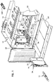
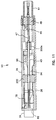
- a jack module 10 according to the present invention is shown in a position to be inserted within a chassis 12.
- a jack plug 14 is shown in a position to be inserted into the jack module 10.
- a rear interface 400 is shown inserted within chassis 12.
- a rear interface plug 520 is shown in a position to be inserted into the rear interface 400.
- the chassis 12 includes sheet metal top and bottom walls 16,18 joined by side walls (only one of which is show at 20) and having sheet metal dividing walls 22.
- a front cover 24 is provided pivotally secured to the side walls 20 to permit the front cover 24 to be pivoted to a down position (shown in Fig. 1) thereby providing access to the interior of the chassis 12.
- the front cover 24 may be pivoted to an up position to cover the interior of the chassis 12.
- Slide attachment blocks are secured within the chassis 12.
- the slide attachment blocks are dielectric and include a lower block 26 and an upper block 28.
- the blocks 26,28 include locking tabs 27 received within slots 29 in walls 16,18 to lock the blocks 26,28 to the interior opposing surfaces of wall 18,16, respectively.
- the blocks 26,28 have vertically aligned grooves 30 sized to receive rails 32 on the jack module 10.
- the rails 32 permit jack module 10 to be slidably received with the chassis 12 in a vertical disposition (as shown in Fig. 1).
- Each of blocks 28,26 cooperate to present grooves 30 sufficient to receive four jack modules 10.
- a jack module 10 is secured within the blocks 26,28 by locking tabs 34. It will be appreciated that slidably received jack modules with locking tabs 34 form no part of this invention per se. Examples of such are shown in commonly assigned U.S. Patent No. 4,840,568.
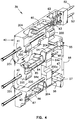
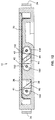
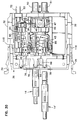
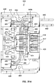
- Fig. 5 and 6 taken in combination, show an exploded perspective view of the jack module 10 which is shown assembled with cover removed in Figs. 2 and 3.
- the module 10 includes a housing 36 and a cover 38 (see Figs. 7-8).
- housing 36 and cover 38 are preferably formed of diecast zinc.
- a dielectric insert 40 is provided sized to be received within the housing 36. As will be more fully described, insert 40 supports various electrical components in a desired orientation as a subassembly 39 (Fig. 4).
- module 10 The internal components of module 10 include forward center coax conductors 41, 42 and 43 and rear coax center conductors 44 and 45.
- Inductor wires 46,47 are provided for joining coax conductors pairs 42,44 and 43,45, respectively.
- Insulators 48,49 are provided for supporting rear coax center conductors 44,45.
- Sleeves 50,51 are provided to permit attachment of the module 10 to a rear interface 400 (as will be more fully described).
- the subassembly 39 includes power source contacts or conductor pins 52,53 (shown best in Figs. 5, 28 and 29), an OUT normal spring 54, an IN normal spring 56 and an inductive cross-connect wire 58.
- the electrical components further include springs 60,61.
- Pins 52,53 are identical. Pin 52 is shown in Figs. 28-29. Pin 52 has a stop 52a and an annular ridge 52b. A pin and 52c extends from stop 52a. A cut-out 52d is provided on an opposite end. Leads 60a (Fig. 5) of spring 60 are placed and soldered within cut-out 52d. Similarly, lead 61a of spring 61 is secured to pin 53.
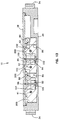
- a first resistor 62 is provided for connecting the monitor (hereinafter "MON") coax conductor 41 with the OUT coax conductor 42 as will be more fully described.
- a second resistor 64 is provided for connecting the MON coax conductor 41 to ground by attachment of the second resistor 64 to a grounding clip 66 received within a slot 68 formed in housing 36.
- a main ground spring 70 (shown best in Figs. 6 and 26) is provided having clip ends 72 sized to be received within slots 74 formed in housing 36. Reception of the clip ends 72 within slots 74 results in mechanical and electrical connection of the grounding spring 70 to the housing 36 (which is electrically grounded upon connection to a grounded rear interface 400 as will be described).
- the grounding spring 70 has spring contact ends 76, 77 and 78 disposed to be in sliding electrical contact with a plug (such as plug 14 of Fig. 1) received within the MON port 80, the OUT port 81 and the IN port 82, respectively, of housing 36.
- the electrical elements supported by the dielectric insert 40 include an OUT termination spring 84 and an IN termination spring 86.
- a third resistor 88 (Fig. 6) is provided to electrically connect the OUT termination spring 84 with the grounding spring 70.
- a fourth resistor 90 is provided to electrically connect the IN termination spring 86 with the main grounding spring 70.
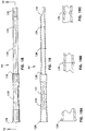
- the components of the jack module 10 include a MON cam 92, an OUT cam 94 and an IN cam 96 all of which are dielectric.
- MON cam 92 is pivotally connected to housing 36 through a first pivot pin 98.
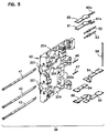
- IN cam and OUT cam 96,94 are both pivotally connected to housing 36 through a second pivot pin 100 received within a bore 102 (Fig. 9). Shown in Fig. 6, a bore 102 is shown for receiving pivot pin 100 and a bore 101 receives pin 98.
- Screws 104 (Fig. 8) are provided for securing cover 38 to housing 36 by passing the screws 104 through holes 106 in cover 38 and receiving the screws 104 in aligned bores 108 formed in housing 36.
- Plastic attachment latches 110 (Fig. 27) are provided received within grooves 112 of housing 36.
- the attachment latches 110 include rails 32 for slidably receiving the module 10 within the chassis 12.
- the latches 110 also include the locking tabs 34 for locking the module 10 in place within the chassis 12.
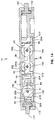
- Fig. 4 shows a subassembly 39 including the insert 40, the MON forward center conductor 41, the OUT forward center conductor 42 and the IN forward center conductor 43 illustrating how the conductors 41-43 are supported by the insert 40.
- the conductors 52,53 are shown supported as are the OUT and IN termination springs 84,86 and the OUT and IN normal springs 54,56.
- Springs 54, 56, 84, 86 are retained within slots 55, 57, 85, 87 formed in insert 40.
- Springs 60,61 are supported in slots 63 formed in insert 40.
- the springs 60,61 are electrically connected (e.g. by solder) to pins 52,53.
- the complete assembly of components is shown inserted within the housing 36 in Fig. 3. In Fig. 3, cover 38 is removed.
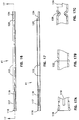
- Each of forward center conductors 41, 42 and 43 are identical. Conductor 41 is shown in greater detail in Fig. 16-17C. A description of conductor 41 will suffice as a description of conductors 42 and 43.
- the conductor 41 is a generally tubular conductive material.
- the conductor 41 is half hard phosphor bronze seamless tube having a nominal wall thickness of about .005 inches.
- the conductor 41 is plated to enhance electrical communication with a spring contact (as will be described).
- the conductor 41 has a flared end 116 extending into an inwardly tapered portion 117.
- a center conducting pin of a plug 14 is inserted through flared end 116 and received within inwardly tapered portion 117.
- the tapered portion 117 has axial slots 119 to permit portion 117 to expand and receive pin 120 (see Fig. 30A).
- the inward taper provides releasable mechanical and electrical contact between the conductor 41 and the center pin 120.
- Annular ridge 122 on conductor 41 permit positive placement of the conductor 41 in insert 40.
- the rear end of conductor 41 is provided with a cut-out 124 to permit placement of a wire (such as inductor wires 46,47) within conductor 41.
- a wire so placed may be soldered to conductor 41.
- An inwardly protruding annual dimple 126 prevents excessive solder flow from cut-out 124 into the interior of tubular conductor 41.
- rear conductor 44 is shown.
- Rear conductor 44 is identical to rear conductor 45 and a description of one will suffice as the description of the other.
- Conductor 44 is formed of materials and plating similar to that of conductor 41 as previously described.
- Rear conductor 44 includes a flared end 128 followed by an inwardly projecting tapered portion 130 having axial slots 131. Similar to tapered portion 117 of conductor 41 (see Figs. 16 and 17), tapered portion 130 receives a center conducting pin (not shown) in slidable mechanical and electrical contact.
- the conductor 44 also includes an opposite cut-out end 132 to receive a wire such as inductor wire 46,47 to be soldered in place. Inwardly projecting annular dimple 134 prevents excessive solder flow into conductor 44.
- the conductor 44 includes an annular ridge 136 and a stop surface 138. Ridge 136 and stop surface 138 cooperate to retain an insulator such as insulator 48,49 between ridge 136 and stop surface 138.
- forward IN conductor 43 is electrically connected to rear IN conductor 45 through IN inductor wire 47.
- forward OUT conductor 42 is electrically connected to rear OUT conductor 44 through OUT inductor wire 46.
- the first resistor 62 is electrically connected to the OUT conductor 42 and the OUT forward center conductor 41.
- MON cam 92 is identical to cams 94 and 96. Accordingly, a description of cam 92 will suffice as a description of cams 94,96.
- the cam 92 has a centrally extending bore 92c extending through a lever body 92e.
- the bore 92c is sized to receive pin 98 (or, in the case of cams 94,96, pin 100).
- the cam includes a cam surface 92a disposed on one side of bore 92c. Disposed on the opposite side of bore 92c is a plunger 92b.
- cam 92 is disposed for surface 92a to be engaged by a plug (such as plug 14 in Fig. 1) inserted within MON port 80.
- the plug pushes against surface 92a causing the cam 92 to pivot around pin 98 (or pin 100 in the case of cams 94,96).
- the plunger 92b urges the springs 60,61 together into electrical contact to close a circuit indicating insertion of a plug into the MON port 80.
- OUT cam 94 is provided with its cam surface 94a disposed to be engaged by a plug inserted within OUT port 81 to cause plunger 94b to urge OUT termination spring 84 against OUT normal spring 54.
- IN cam 96 is disposed for its cam surface 96a to be engaged by a plug inserted within IN bore 82 to urge cam 96 to pivot about pin 100 with plunger 96b urging IN termination spring 86 against IN normal spring 56.
- the plunger 92b is provided with a slot 92d to permit unobstructed movement of the plunger without interference with conductor 41.
- plungers 94b and 96b are provided with slots 94d and 96d to prevent interference with conductors 42 and 43, respectively.
- Springs 54 and 56 are provided with normal contact points 54a, 56a (see Fig. 4) disposed to electrically engage conductors 42,43, respectively.
- Cross-connect wire 58 (see Fig. 3) electrically connects springs 56 and 54. Accordingly, in the absence of any plug inserted within ports 81,82, conductors 42 and 43 are electrically connected.
- coaxial conductors provide for a central conductor surrounded by a grounded shield.
- the present invention utilizes the geometry of the zinc housing 36 and zinc cover 38 to provide the grounded shield. This results in minimized volume of the module 10.
- the housing is provided with concave arcuate surfaces 150.
- the cover 38 (Fig. 7) has concave arcuate surfaces 152.
- the surfaces 150,152 are disposed to at least partially surround conductors 41-45 when cover 38 is placed on housing 36. As a result, the surfaces 150,152 cooperate to define grounded shields at least partially surrounding conductors 41-45.
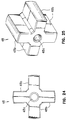
- the impedance of the system is controlled by controlling the geometry of dielectric supports 200 on insert 40.
- the supports 200 are most clearly visible in Figs. 4 and 5. As shown, the supports 200 are generally rectangularly shaped and are connected via cross-beams 201 to platforms 204 of insert 40. Support 200a joins two platforms 204. Comparing Figs. 4 and 14, the platforms 204 are sized to be received within platform pathways 210 formed in housing 36.
- the nesting of the insert 40 within housing 36 is best shown in Figs. 11-15.
- the surfaces 150 cooperate with surfaces 152 to define partially cylindrical chambers through which the conductors 41-43 pass.
- the dielectric support blocks 200 are received in a portion of the partially cylindrical chambers.
- the support blocks 200,200a are connected to the platforms 204 via cross bars 201. It will be recognized by those skilled in the art that by varying the geometry of the supports 200,200a, the impedance of the system can be tuned to a desired impedance.
- dielectric spacers 48,49 In addition to supporting the conductors 41-43 in supports 200,200a, rear conductors 44,45 are supported in dielectric spacers 48,49 as shown in Fig. 11.
- the spacers 48,49 are housed in a cylindrical portion of sleeves 50 and 51.
- Dielectric support spacers 48,49 of the geometry shown are also shown in U.S. Patent No. 4,749,968 (items 250 in the figures of that patent) which indicates that the spacers can be selected to assist in tuning the system to a desired impedance.
- Spacers 48,49 are identical. Spacer 48 is shown in Figures 24 and 25.
- the spacer 48 includes a bore 48a for receiving conductor 44 and radially spaced ribs 48b.
- the conductors 42, 43, 44 and 45 cooperate with the inductors 46,47 and insulators 48,49 and supports 200,200a to create a desired impedance. Notwithstanding this tuning, the presence of springs 56,54 can result in an imbalanced or undesired impedance for the module 10. With best reference to Fig. 3, it is noted that springs 54,56 reside generally parallel to conductors 42,43 and inductors 46,47. As a result of this parallel geometry, a first capacitance is generated between spring 56 and conductor 43 and a second capacitance is generated between spring 54 and conductor 42. To balance these capacitances, an inductance is provided via conductor 58.
- the specific gage of conductor 58 is selected to balance the capacitance resulting from the spacial relation of spring 56, inductor 47, conductor 43 and spring 54, conductor 42 and inductor 46.
- the inductance of inductors 46,47 and cross-wire 58 are matched with the capacitance of springs 54,56 to provide impedance matching.
- a plug 14 is shown in Fig. 30A.
- the plug 14 includes a central conductor 300 terminating at central pin 120.
- the conductor 300 has a central exposed slot 302 for receiving a central conductor 304 of a coax cable 306.
- a crimp connection 308 is provided for crimping the shield of the coax cable 306 to an outer-conductive shield 310.
- the shield 310 narrows to a plug end 312 surrounding central pin 120.
- a portion of shield 310 is removed to provide an access opening 320 to permit wire 304 to be laid into slot 302 and secured through any suitable means such as soldering and the like.
- Fig. 30 shows the module (cover removed) with plugs 14,14' fully inserted into the OUT port 81 and positioned to be inserted into the IN port 82.
- the cam 94 is urged to force the spring normal contact 54 away from the central conductor 42. Since the plug 14' is not yet inserted into the IN port 82, the cam 96 has not been moved to urged the IN normal spring 56 away from the OUT conductor 43.
- rear interface 400 includes a housing 402 consisting of a housing body 404 and a housing cover 406.
- the housing body 404 has rails 408 sized to be received within grooves 30. Accordingly, rear interface 400 may be slid into grooves 30 to the rear of blocks 26,28 and snap fit in place.
- the housing 402 has the approximate width of jack module 10.
- Opposing surfaces of body 404 and cover 406 cooperate to define a rear interface interior which contains a plurality of components.
- the components include a dielectric support platform 410, (shown separately in Fig. 33) a grounding spring 412 (Fig. 40), an OUT pin conductor 414 (Fig. 38) and an IN pin conductor 416.
- the internal components also include an OUT pin receiving conductor 418 (Fig. 37), an IN pin receiving conductor 420, a first plug receiving conductor 422 (Fig. 36) and a second plug receiving conductor 424.
- the components still further include an OUT spring 426, an IN spring 428, and a connecting conductor 430.
- the components still further include four pin receiving conductors 432, 434, 436, 438, two wire wrap pins 440,442 (one of which is shown in Fig. 39) and OUT dielectric cam 444 and IN dielectric cam 446.
- Screws 448 are provided to be received within a aligned holes 450 of cover 406 and body 404 to connect cover 406 to body 404 and enclose the interior components of the rear interface 400.
- body 404 and cover 406 are both electrically conductive and, preferably, are formed of die cast zinc.
- the ground spring 412 is provided with clip ends 451 sized to be received within slots 452 formed in body 404. Reception of the clip ends 451 within slots 452 results in mechanical and electrical connection of the grounding spring 412 to the housing body 404 (which is electrically grounded upon connection of patch plug with coax conductor to the interface 400).
- the grounding spring 412 has spring contact ends 454,455 disposed to be within sliding electrical contact with sleeves 50,51, respectively, when received within a first OUT port 458 and a first IN port 460, 0respectively, formed in body 404.
- Pins 414,416 are received within holes 462,464, respectively, formed in dielectric insert 410.
- Pin 414 is shown enlarged in Fig. 38. Since pin 414 is identical to pin 416, a description of one will suffice as a description of the other.
- the pin 414 includes an elongated pin contact 466. On an opposite end of pin 414, a cutout 468 is provided. Cutout 468 permits reception of a conductor which may be soldered into cutout 468 in a manner previously described with respect to the conductors of jack module 10.
- a first annular rib 470 is provided adjacent cutout 468. Between rib 470 and pin end 466, an annular ring 472 is provided. Pin 414 is inserted into hole 462 with the ring 472 providing accurate placement and with rib 470 press fit into hole 462 to securely hold pin 414 in place.
- Pins 414 and 416 are disposed and sized to be received within conductors 44,45 of jack module 10 when sleeves 50,51 are received within ports 458,460. Accordingly, pins 414,416 become electrically connected to conductors 44,45.
- pin receiving conductors 418,420 are received within the bores 476,478 of insert 410.
- Pin receiving conductor 418 is shown enlarged in Fig. 37. It will be appreciated that pin 418 is identical to pin 420 and a description of one will suffice as a description of the other.
- the pin receiving conductor 418 is generally cylindrical and hollow and includes a tapered pin receiving end 482. Opposite end 482, a cutout 484 is provided to permit placement of a conductor which may be soldered into cutout 484 in a manner previously described. Rib 486 is disposed adjacent cutout 484. Spaced from rib 486 on a side opposite of cutout 484 is an annular ring 488. Rib 486 and ring 488 serve the similar function as rib 470 and ring 472 of pin conductor 414. With the pin receiving conductors 418 received within holes 476,478, inductors 477,479 are placed spanning and electrically connecting pin 414, pin receiving conductor 418, and pin 416 and pin receiving conductor 420 respectively. Conductors 418,420 are coaxially disposed within second OUT port 459 and second IN port 461, respectively.
- a pin receiving conductor 422 is shown enlarged in Fig. 36.
- Pin receiving conductor 422 is generally cylindrical and includes an inwardly-tapered plug receiving end 490. Pin receiving end is sized to receive a pin (not shown) of any standard plug which may be inserted within end 490.
- An opposite end of pin receiving conductor 422 includes a cutout 492 which receives a conductor which is soldered within cutout 492.
- a sleeve 494 is provided to permit press fitting of conductor 422 into a bore 496 of insert 410.
- pin receiving conductor 424 is received within bore 498 of dielectric insert 410.
- Wire wrap pins 440,442 are identical. Shown in Fig. 39, pin 440 includes wire wrap end 440a and fastening barb 440b. The barb 440b, is received within slot 500 formed in dielectric insert 410. Similarly, pin 442 is received within slot 502.
- the ground pin receiving conductors 432, 434, 436, and 438 are identical in construction to conductors 418,420 and are press fit into bores 432a, 434a, 436a, and 438a of dielectric insert 410.
- Conductors 432,434 are disposed to receive pins 52,53 when sleeves 50,51 are received within bores 458,460, respectively.
- Pin receiving conductors 436,438 are disposed to receive pins 53,52 when jack module 10 is rotated 180° with sleeve 50 received within bore 460 and with sleeve 51 received within bore 458.
- Symmetrical positioning of pin receiving conductors 432, 434, 436, and 438 about a central axis X-X of rear interface 400 permits jack module 10 to be inserted in one of two orientations to permit monitoring of either the IN or the OUT conductors at the option of a user.
- Conductors 433,439 electrically connect the pin receiving conductor 432,438, respectively, with the wire wrap pin 440.
- Conductors 435,437 connect the pin receiving conductors 434,436, respectively, with wire wrap pin 442.
- plug receiving conductors 422,424 are connected to pin 442 via conductors 423,425.
- OUT spring 426 is received within a slot 504 in dielectric insert 410.
- IN spring 428 is similarly received within a slot 506.
- the springs 426,428 are sized and positioned to be biased against pin conductors 414,416, respectively.
- Cam 444 is pivotably positioned to be urged by a sleeve (such as sleeve 50 or 51) received within bore 458 to urge spring 426 away from pin conductor 414 and thereby break electrical connection between spring 426 and pin conductor 414.
- cam 446 is pivotably positioned to be urged by a sleeve (such as either sleeve 50 or 51) received within bore 460 to urge spring 428 away from and out of electrical connection with pin 416.
- the connecting conductor 430 electrically connects springs 426,428.
- the dielectric insert 410 includes a generally flat bottom platform 510.
- Bottom platform 510 is sized to be received within and rest against an outer wall 512 (see Fig. 35) of main body 404.
- the components are properly aligned with pins 414,416 centrally received within bores 458,460.
- Grounding spring ends 454,455 are disposed within bores 458,460 to electrically engage a sleeve (such as sleeves 50,51) received within bores 458,460.
- Pin receiving conductors 432, 434, 436, 438 are properly disposed to receive pins 52,53 depending on the orientation of the jack module 10 as previously described.
- the body 404 and cover 406 are provided with a plurality of arcuate surfaces 514.
- the arcuate surfaces 514 are disposed to at least partially surround coax conductors 418, 420, 414, and 416. More accurately, the conductors 414, 416, 418 and 420 become central conductors surrounded by the grounded shields of the arcuate surfaces 514.
- the rear interface 400 utilizes the geometry of the zinc body 404 and cover 406 to provide the grounded shield for the coax conductors.
- the presence of springs 426,428 in generally parallel alignment to pin conductors 414,416, can result in an imbalanced or undesired impedance for the rear interface 400.
- a third capacitance is generated between the spring 426 and pin conductor 414.
- a fourth capacitance is generated between spring 428 and pin conductor 416.
- the gauge of cross-conductor 430 is selected to balance these capacitances. Namely, the cross-conductor 430 acts as an inductor to balance the capacitances.
- the specific gauge is selected to balance the capacitance resulting from the spacial relation of the springs 426,428 and the conductors 414,416.
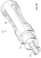
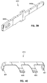
- Figs. 41-44 illustrate a patch plug 520 for electrically connecting a coax cable (not shown) to the rear of interface 400 by connection to pin receiving conductors 418,420.
- the patch plug 520 includes a generally cylindrical outer jacket 522.
- a barbed insert 524 is provided sized to be received within the interior of jacket 522.
- the elements of the patch plug further include a central coax conductor pin 526, dielectric spacers 528, first and second cooperating crimping members 530,532, and a rear retaining sleeve 534.
- a coax cable 600 with central conductor 602 and grounded sleeve 604 are connected to patch plug 520.
- barbed insert 524 is slidably received within outer jacket 522.
- the barbed insert has diametrically opposed arcuate and projecting barbs 536. Projecting outwardly from barbs 536 are protruding and angularly ramped locking tabs 538. Tabs 538 project through slots 540 formed in a reduced diameter portion 521 of outer jacket 522. Reduced diameter portion 521 is sized to be received within rear ports 459,461 (see Fig. 32) formed in housing body 404.
- body 404 and housing cover 406 are provided with annular grooves 517.
- the locking tabs 538 are disposed to be received within grooves 517 to retain plug 520 from axial movement relative to the housing 404 while permitting rotational movement.
- the pin 527 of pin conductor 526 is disposed to be received within pin receiving conductors 418,420.
- the insulators 528 retain the pin 526 in concentric spaced relation to the conductive insert 524 and conductive outer jacket 522.
- the pin includes a conductor receiving bore 552 sized to receive a central conductor 602 of a commercially available coaxial cable.
- the grounded shield of the coaxial cable 600 is placed between opposing surfaces of crimping members 530,532 after which outer crimping member 532 may be crimped against inner crimping member 530 to securely connect the grounding shield of the coaxial cable to the conductive outer jacket 520 in insert 524.
- the rear retaining sleeve 534 may be connected to the insulated sheeting of the coaxial cable with the rear retaining sleeve 534 connected to insert 524 by cooperating threads on the exterior of rear connecting sleeve 534 and the interior of insert 524.
- the patch plug 520 is inserted into bores 514 by simply axially thrusting the plug 520 into bores 514 with pin 527 electrically and mechanically received within either of pin receiving conductors 418,420. Flexibility of the barbs 536 permits tabs 538 to flex inwardly to permit insertion. The tabs 538 then flex outwardly to be captured within annular grooves 517. To retract the plug, an operator simply pulls on outer jacket 522. A slot defining edge 541 (Fig. 44) on reduced diameter portion 521 urges against the ramp of tabs 538 to force the tabs 538 inwardly out of their locking position in grooves 517. This permits removal of the patch plug.
- the body 404 and cover 406 are electrically grounded. Likewise, the housing 36 and cover 38 of module 10 are grounded.
- the interface 400 is inserted within grooves 30 of chassis 12 to the rear portion of blocks 28,26.
- Coaxial cables (not shown) previously connected to patch plugs, such as plugs 520, are connected to the rear interface 400 by inserting an OUT coax cable into port 459 and an IN coax cable into port 461.
- the coaxial cables are electrically interconnected by reason of the electrical circuit from conductor 414, through springs 426,428 and conductor 430 to conductor 416 (Fig. 31A).
- Tracer lamp jacks are plugged into either sleeves 422,424. Power is provided by connection of voltage source and ground (not shown) to pins 440,442.
- arcuate surfaces 152, 150, 514 formed on the interior of the jack module 10 and rear interface 400 provide shielded grounding surrounding central coax conductors upon connection of a grounded cable to interface 400.
- the surfaces cooperate with the conductors to provide proper impedance matching to achieve a desired 75 ohm impedance.
- cross-conductor 58 and cross-conductor 430 are selected to have an inductance to tune the capacitive effect of springs 54, 56, 426, 428 aligned in parallel to the coax conductors.
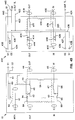
- the precise surfaces and geometry of the surfaces and size of conductors 58,430 may be empirically selected. However, certain parameters for impedance matching are recognized in the art. To assist in a complete understanding of the present invention, a discussion of those follows.
- Impedance is defined as the total passive opposition offered to the flow of alternating current.
- the impedance of the source, the load, and the transmission cable and connectors must be the same. The greater the variation, the less efficient the transfer of energy becomes.
- As a pulse or wave travels down a transmission line there is generally no problem as long as the impedance remains constant. However, when a section of different impedance is encountered, such as a poorly designed connector or distorted cable, a portion of the wave is reflected back toward the source resulting in a loss of power and/or distortion of the signal.
- the presence of an inductor in a circuit causes a counter electromotive force which, in addition to resistance, further opposes the flow of current.
- An inductor alone in a circuit causes the current to lag the voltage by a phase angle equal to 90° (see Figs. 47A-47C).
- the impedance of the circuit is then greater than when it included resistance alone.
- the amount of increase in the impedance is equal to the inductive reactance.
- a capacitor in a circuit also causes an electromotive force that opposes the flow of current in a circuit.
- a capacitor alone in a circuit causes the voltage to lag the current by a phase angle equal to 90° (see Figs. 48A-48C).
- a capacitor changes the impedance of a circuit, but unlike an inductor, a capacitor decreases the impedance of the circuit by an amount equal to the capacitive reactance.
- VSWR Voltage Standing Wave Ratio
- Refl Coeff Reflection Coefficient
- Impedance measurement methods include return loss using a spectrum analyzer with a directional bridge, or a TDR ("time domain reflectometer") impedance profile using a time domain reflectometery.
- the spectrum analyzer will measure return loss in decibels over a selected frequency spectrum.
- the time domain reflectometer measures the impedance and displays a profile that indicates inductive and capacitive reactances.
- the circuit in Fig. 49A is inductive (E L and X L predominant), and the circuit in Fig. 50A is capacitive (E C and X C predominant). It is important to note that the capacitance reduces the overall impedance and inductance increases the overall impedance as illustrated in the figures shown.
- Tuning refers to the variation of the capacitance or inductance, thus a variation in the capacitive or inductive reactance, in order to achieve a desired overall impedance and phase angle.
- Dielectric material is the insulating material which will store but not conduct electricity.
- a dielectric material's ability to store electrostatic energy, compared to this same storing ability for air is defined as the materials's dielectric constant.
- the dielectric constant for air is one.
- This equation may be further modified to compensate for an eccentric or doubly eccentric centerline.
- the foregoing equations may be combined to mathematically compute the inductance for the module 10 and rear interface 400.
- the central conductors 41, 42, 43 pass through outer conductors ( i.e. , the opposing surfaces of housing 36 and cover 38) which have a varying geometry.
- the space between the conductors 41, 42, and 43 and their surrounding conductive surfaces are partially filled with dielectric material (e.g., blocks 200,200a).
- a capacitor consists of two parallel conductors separated by a dielectric. Each cantilever spring and conductor running parallel to it act as capacitors with point contacts on one end (see Fig. 56).
- the two capacitors are electrically in series with a cross-conductor having an inductance that can be varied for balance and tuning.
- This circuit can be tuned for impedance matching between the 75 ⁇ line and the module conductors which would minimize phase distortion and other losses in the circuit.
- Fig. 45 represents the geometry of springs 54, 56, 426, 428 opposing conductors 42, 43 (with inductors 46, 47), 414 and 416 (with inductors 477, 479). Utilizing the foregoing equations, the necessary inductance of conductors 58,430 can be calculated. The final gauge and inductance of conductors 58,430 may be further modified in response to a measured impedance until a final desired impedance is attained.
- DSX modules can be greatly reduced by the teachings of the present invention. So reduced, a higher density of DSX modules may be installed in a given system. Further, individual modules 10 may be paired in a common circuit to provide multiple position porting on the forward end.
- the jack module 10 does not, by itself, comprise complete DSX circuit. Instead, the jack module may be paired with an additional jack module to form a completed circuit. Further, the utilization of the normally closed rear interface circuit permits the use of the module in a digital distribution function such as that shown and described in commonly assigned and copending U.S. Patent Application Serial No. 07/614,143 filed November 15, 1990, and entitled "Digital Distribution Apparatus.”
Landscapes
- Engineering & Computer Science (AREA)
- Computer Networks & Wireless Communication (AREA)
- Coupling Device And Connection With Printed Circuit (AREA)
- Details Of Connecting Devices For Male And Female Coupling (AREA)
- Control Of Motors That Do Not Use Commutators (AREA)
- Multi-Conductor Connections (AREA)
- Communication Cables (AREA)
- Cable Accessories (AREA)
- Input Circuits Of Receivers And Coupling Of Receivers And Audio Equipment (AREA)
Abstract
- an insert (524) with opposing spring members (536) having tabs (538) that project radially outward from the insert member (524); a jacket (522) which is telescopically movable relatively to the insert between a first position in which the tabs (538) project through openings (540) in the jacket, and a second position in which the tabs (540) are retracted within the jacket; a conductor pin (526) mounted within the insert (524) and constructed and arranged to be connected to a coaxial cable; and structure (530, 532, 534) for securing the coaxial cable (600) within the insert (524).
Description
- This invention pertains to the telecommunications industry. More particularly, this invention pertains to a coaxial cable plug for use in said industry.
- As is commonly known in the telecommunications industry, high speed signal transmission rates require coaxial conductors. For example, so-called DS-3 signal rates (i.e., 44.736 megabits per second) are carried over coax cables.
- In order to permit cross-connection, line monitoring and line access, the industry has utilized so-called DSX-3 coax jack modules to permit interconnection, cross-connection and the like. An example of such a module is shown in U.S. Patent No. 4,815,104. As shown in the aforesaid U.S. Patent No. 4,815,104, the module includes internal switching assemblies (
items items items - In the telecommunications industry, it is standard for a cross-connect system to operate at 75 ohms. Accordingly, the prior art modules are designed and constructed to have a 75 ohm impedance.
- In the telecommunications industry, a central office or other location will have a substantial number of cross-connect modules arranged in bays. Due to the large volume required to house such modules and bays, it is becoming increasingly desirable to miniaturize DSX modules. Such miniaturization should permit switching, access and monitoring functions while maintaining desired impedance levels.
- It is an object of the present invention to provide a miniaturized DSX-3 jack module. According to a preferred embodiment of the present invention, this object is achieved by providing a coax jack module having first and second coax conductors. A first conductive spring contact is biased into electrical contact with the first conductor and cooperates with the first conductor to generate a first capacitance. A second conductive spring contact is provided biased into electrical contact with the second conductor and cooperates with the second conductor to generate a second capacitance. An internal conductor electrically connects the first and second spring contacts. The internal conductor has an inductance selected to cooperate with the first and second capacitance for the jack to have the desired impedance. The object of the invention is further achieved by a jack module having grounded internal surfaces at least partially surrounding the module's internal conductors. The surfaces act as the grounding shield for coax conductors.
-
- Fig. 1 is a perspective view showing a jack module according to the present invention in exploded relation to a chassis for receiving such module;
- Fig. 2 is a perspective view of a jack module with a cover removed to exposed internal elements;
- Fig. 3 is a side elevation view of the jack module of the present invention with a cover removed to show internal elements;
- Fig. 4 is a perspective view of a subassembly of the jack module of the present invention;
- Fig. 5 is a perspective exploded view of the subassembly of Fig. 4;
- Fig. 6 is a perspective exploded view of the jack module less cover and the subassembly of Fig. 4;
- Fig. 7 is a perspective view of a cover for the jack module showing an interior surface of the cover;
- Fig. 8 is a perspective view of the cover of Fig. 7 showing an external surface and screws shown exploded;
- Fig. 9 is a perspective view of a housing of the jack module showing an interior surface of the housing;
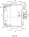
- Fig. 10 is a side elevation view of the assembled jack module of the present invention;
- Fig. 11 is a view taken along line 11-11 of Fig. 10;
- Fig. 12 is a view taken along line 12-12 of Fig. 10;
- Fig. 13 is a view taken along line 13-13 of Fig. 10;
- Fig. 14 is a view taken along line 14-14 of Fig. 10;
- Fig. 15 is a view taken along line 15-15 of Fig. 10;
- Fig. 16 is a top plan view of a forward center conductor for use with the present invention;
- Fig. 17 is a view taken along line 17-17 of Fig. 16;
- Fig. 17A is an enlarged view of a left end of the conductor of Fig. 17;
- Fig. 17B is an enlarged central portion of the conductor of Fig. 17;
- Fig. 17C is an enlarged view of a right end of the conductor of Fig. 17;
- Fig. 18 is a top plan view of a rear center conductor for use with the present invention;
- Fig. 19 is a view taken along line 19-19 of Fig. 18;
- Fig. 19A is an enlarged view of a left end of the conductor of Fig. 19;
- Fig. 19B is an enlarged central portion of the conductor of Fig. 19;
- Fig. 19C is an enlarged view of a dimpled portion of the conductor of Fig. 19;
- Fig. 20 is a left side, bottom and rear perspective view of a cam for use with the present invention;
- Fig. 20A is a rear, left side and top perspective view of the cam of Fig. 20;
- Fig. 21 is a left side elevation view of the cam of Fig. 20;
- Fig. 22 is a right side, bottom and front perspective view of the cam of Fig. 20;
- Fig. 23 is a right side, top and front perspective view of the cam of Fig. 20;
- Fig. 24 is a front elevation view of a dielectric support;
- Fig. 25 is a perspective view of the support of Fig. 24;
- Fig. 26 is a perspective view of a grounding spring;
- Fig. 27 is a perspective view of an attachment latch;
- Fig. 28 is a top plan view of a conductor pin;
- Fig. 29 is a view taken along line 29-29 of Fig. 28;
- Fig. 30 is a top plan view of the jack of the present invention with cover removed to show internal elements and with a first plug shown inserted and a second plug shown about to be inserted;
- Fig. 30A is a cross-sectional view of a plug;
- Fig. 31 is a front, top and right side perspective view of a rear interface for a coax jack module of the present invention;
- Fig. 31A is a side elevation view of the rear interface with a cover removed to exposed interior elements;
- Fig. 32 is an exploded perspective view of the rear interface of Fig. 31;
- Fig. 33 is an enlarged perspective view of a dielectric support for the rear interface of Fig. 31;
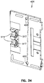
- Fig. 34 is an inside perspective view of a cover for the rear interface of Fig. 31;
- Fig. 35 is a perspective interior view of a housing body for the rear interface of Fig. 31;
- Fig. 36 is a perspective view of a pin receiving conductor for use with the rear interface of Fig. 31;
- Fig. 37 is a perspective view of a pin receiving conductor for use with the rear interface of Fig. 31;
- Fig. 38 is a pin conductor for use with the rear interface of Fig. 31;
- Fig. 39 is a perspective view of a wire wrap pin for use with the rear interface of Fig. 31;
- Fig. 40 is a perspective view of a grounding spring for use with the rear interface of Fig. 31;
- Fig. 41 is a perspective view of a patch plug for use with the rear interface of Fig. 31;
- Fig. 42 is a side elevation view of the patch plug of Fig. 41;
- Fig. 43 is an exploded perspective view of the patch plug of Fig. 41;
- Fig. 44 is an assembled cross-sectional view of the patch plug of Fig. 41;
- Fig. 45 is an electrical schematic of the circuitry of the jack module and rear interface; and
- Figs. 46-56 are schematic drawings illustrating the analysis of tuning the module of the invention to a desired impedance.
- Referring now to the several drawing figures in which identical elements are numbered identically throughout, a description of the preferred embodiment will now be provided.
- In Fig. 1, a
jack module 10 according to the present invention is shown in a position to be inserted within achassis 12. Ajack plug 14 is shown in a position to be inserted into thejack module 10. Arear interface 400 is shown inserted withinchassis 12. Arear interface plug 520 is shown in a position to be inserted into therear interface 400. - As shown in Fig. 1, the
chassis 12 includes sheet metal top andbottom walls metal dividing walls 22. Afront cover 24 is provided pivotally secured to theside walls 20 to permit thefront cover 24 to be pivoted to a down position (shown in Fig. 1) thereby providing access to the interior of thechassis 12. Thefront cover 24 may be pivoted to an up position to cover the interior of thechassis 12. - Slide attachment blocks are secured within the
chassis 12. The slide attachment blocks are dielectric and include alower block 26 and anupper block 28. Theblocks tabs 27 received withinslots 29 inwalls blocks wall - The
blocks grooves 30 sized to receiverails 32 on thejack module 10. Therails 32permit jack module 10 to be slidably received with thechassis 12 in a vertical disposition (as shown in Fig. 1). - Each of
blocks grooves 30 sufficient to receive fourjack modules 10. Ajack module 10 is secured within theblocks tabs 34. It will be appreciated that slidably received jack modules with lockingtabs 34 form no part of this invention per se. Examples of such are shown in commonly assigned U.S. Patent No. 4,840,568. - Fig. 5 and 6, taken in combination, show an exploded perspective view of the
jack module 10 which is shown assembled with cover removed in Figs. 2 and 3. Themodule 10 includes ahousing 36 and a cover 38 (see Figs. 7-8). For reasons that will become apparent,housing 36 and cover 38 are preferably formed of diecast zinc. - A
dielectric insert 40 is provided sized to be received within thehousing 36. As will be more fully described, insert 40 supports various electrical components in a desired orientation as a subassembly 39 (Fig. 4). - The internal components of
module 10 include forward center coaxconductors coax center conductors Inductor wires Insulators coax center conductors Sleeves module 10 to a rear interface 400 (as will be more fully described). - The
subassembly 39 includes power source contacts or conductor pins 52,53 (shown best in Figs. 5, 28 and 29), an OUTnormal spring 54, an INnormal spring 56 and aninductive cross-connect wire 58. - The electrical components further include
springs Pins Pin 52 is shown in Figs. 28-29.Pin 52 has astop 52a and anannular ridge 52b. A pin and 52c extends fromstop 52a. A cut-out 52d is provided on an opposite end.Leads 60a (Fig. 5) ofspring 60 are placed and soldered within cut-out 52d. Similarly, lead 61a ofspring 61 is secured to pin 53. - A
first resistor 62 is provided for connecting the monitor (hereinafter "MON") coaxconductor 41 with the OUT coaxconductor 42 as will be more fully described. Asecond resistor 64 is provided for connecting the MON coaxconductor 41 to ground by attachment of thesecond resistor 64 to agrounding clip 66 received within aslot 68 formed inhousing 36. - A main ground spring 70 (shown best in Figs. 6 and 26) is provided having clip ends 72 sized to be received within
slots 74 formed inhousing 36. Reception of the clip ends 72 withinslots 74 results in mechanical and electrical connection of thegrounding spring 70 to the housing 36 (which is electrically grounded upon connection to a groundedrear interface 400 as will be described). Thegrounding spring 70 has spring contact ends 76, 77 and 78 disposed to be in sliding electrical contact with a plug (such asplug 14 of Fig. 1) received within theMON port 80, theOUT port 81 and theIN port 82, respectively, ofhousing 36. - The electrical elements supported by the dielectric insert 40 (Fig. 5) include an
OUT termination spring 84 and anIN termination spring 86. A third resistor 88 (Fig. 6) is provided to electrically connect theOUT termination spring 84 with thegrounding spring 70. Similarly, afourth resistor 90 is provided to electrically connect theIN termination spring 86 with themain grounding spring 70. - As will be more fully described, the components of the
jack module 10 include aMON cam 92, anOUT cam 94 and anIN cam 96 all of which are dielectric.MON cam 92 is pivotally connected tohousing 36 through afirst pivot pin 98. IN cam andOUT cam housing 36 through asecond pivot pin 100 received within a bore 102 (Fig. 9). Shown in Fig. 6, abore 102 is shown for receivingpivot pin 100 and abore 101 receivespin 98. Screws 104 (Fig. 8) are provided for securingcover 38 tohousing 36 by passing thescrews 104 throughholes 106 incover 38 and receiving thescrews 104 in alignedbores 108 formed inhousing 36. - Plastic attachment latches 110 (Fig. 27) are provided received within
grooves 112 ofhousing 36. The attachment latches 110 includerails 32 for slidably receiving themodule 10 within thechassis 12. Thelatches 110 also include the lockingtabs 34 for locking themodule 10 in place within thechassis 12. - Fig. 4 shows a
subassembly 39 including theinsert 40, the MONforward center conductor 41, the OUTforward center conductor 42 and the INforward center conductor 43 illustrating how the conductors 41-43 are supported by theinsert 40. Also, theconductors normal springs Springs slots insert 40.Springs slots 63 formed ininsert 40. Thesprings pins housing 36 in Fig. 3. In Fig. 3, cover 38 is removed. - Each of
forward center conductors Conductor 41 is shown in greater detail in Fig. 16-17C. A description ofconductor 41 will suffice as a description ofconductors - The
conductor 41 is a generally tubular conductive material. In a preferred embodiment, theconductor 41 is half hard phosphor bronze seamless tube having a nominal wall thickness of about .005 inches. Theconductor 41 is plated to enhance electrical communication with a spring contact (as will be described). - The
conductor 41 has a flaredend 116 extending into an inwardly taperedportion 117. A center conducting pin of aplug 14 is inserted through flaredend 116 and received within inwardly taperedportion 117. The taperedportion 117 hasaxial slots 119 to permitportion 117 to expand and receive pin 120 (see Fig. 30A). The inward taper provides releasable mechanical and electrical contact between theconductor 41 and thecenter pin 120. -
Annular ridge 122 onconductor 41 permit positive placement of theconductor 41 ininsert 40. The rear end ofconductor 41 is provided with a cut-out 124 to permit placement of a wire (such asinductor wires 46,47) withinconductor 41. A wire so placed may be soldered toconductor 41. An inwardly protrudingannual dimple 126 prevents excessive solder flow from cut-out 124 into the interior oftubular conductor 41. - With reference now to Figs. 18-19C,
rear conductor 44 is shown.Rear conductor 44 is identical torear conductor 45 and a description of one will suffice as the description of the other. -
Conductor 44 is formed of materials and plating similar to that ofconductor 41 as previously described. -
Rear conductor 44 includes a flaredend 128 followed by an inwardly projectingtapered portion 130 havingaxial slots 131. Similar to taperedportion 117 of conductor 41 (see Figs. 16 and 17), taperedportion 130 receives a center conducting pin (not shown) in slidable mechanical and electrical contact. Theconductor 44 also includes an opposite cut-outend 132 to receive a wire such asinductor wire annular dimple 134 prevents excessive solder flow intoconductor 44. Theconductor 44 includes anannular ridge 136 and astop surface 138.Ridge 136 and stopsurface 138 cooperate to retain an insulator such asinsulator ridge 136 and stopsurface 138. - As best shown in Fig. 11, forward IN
conductor 43 is electrically connected to rear INconductor 45 throughIN inductor wire 47. Similarly, forward OUTconductor 42 is electrically connected to rear OUTconductor 44 throughOUT inductor wire 46. Thefirst resistor 62 is electrically connected to theOUT conductor 42 and the OUTforward center conductor 41. - With reference now to Figs. 20-23, a description of
MON cam 92 will be provided.MON cam 92 is identical tocams cam 92 will suffice as a description ofcams - The
cam 92 has a centrally extendingbore 92c extending through alever body 92e. Thebore 92c is sized to receive pin 98 (or, in the case ofcams - The cam includes a
cam surface 92a disposed on one side ofbore 92c. Disposed on the opposite side ofbore 92c is aplunger 92b. - As best shown in Fig. 3,
cam 92 is disposed forsurface 92a to be engaged by a plug (such asplug 14 in Fig. 1) inserted withinMON port 80. The plug pushes againstsurface 92a causing thecam 92 to pivot around pin 98 (or pin 100 in the case ofcams 94,96). As a result, theplunger 92b urges thesprings MON port 80. - OUT
cam 94 is provided with its cam surface 94a disposed to be engaged by a plug inserted within OUTport 81 to cause plunger 94b to urge OUTtermination spring 84 against OUTnormal spring 54. - IN
cam 96 is disposed for its cam surface 96a to be engaged by a plug inserted within IN bore 82 to urgecam 96 to pivot aboutpin 100 with plunger 96b urging INtermination spring 86 against INnormal spring 56. - The
plunger 92b is provided with aslot 92d to permit unobstructed movement of the plunger without interference withconductor 41. Similarly, plungers 94b and 96b are provided with slots 94d and 96d to prevent interference withconductors - As shown in Fig. 3, in the absence of a plug in any of ports 80-82, the
cams springs springs spring 84 separated fromspring 54 and withspring 86 separated fromspring 56. -
Springs normal contact points conductors springs ports conductors - Upon insertion of a plug into
port 82, the electrical connection betweenconductors OUT conductor 42 is connected acrossresistor 90 to ground. A signal on theIN conductor 43 is now connected directly to the plug (not shown) inserted intoport 82. Similarly, upon insertion of a plug (not shown) intoport 81, theIN conductor 43 is connected acrossresistor 88 to ground and theOUT conductor 42 is connected directly to the plug inserted withinport 81. Insertion of a plug intoport 80 results in closing springs 60,61. It will be recognized by those skilled in the art that an electrical schematic of the circuit thus described is common in DSX modules. A schematic of this circuit is shown in Fig. 45. - As is common, coaxial conductors provide for a central conductor surrounded by a grounded shield. The present invention utilizes the geometry of the
zinc housing 36 andzinc cover 38 to provide the grounded shield. This results in minimized volume of themodule 10. - With best reference to Figs. 7, 9 and 12-15, it can be shown how the housing is provided with concave
arcuate surfaces 150. Similarly, the cover 38 (Fig. 7) has concavearcuate surfaces 152. The surfaces 150,152 are disposed to at least partially surround conductors 41-45 whencover 38 is placed onhousing 36. As a result, the surfaces 150,152 cooperate to define grounded shields at least partially surrounding conductors 41-45. - In addition to shielding as a result of arcuate surfaces 150,152 integrally cast into the
housing 36 andcover 38, the impedance of the system is controlled by controlling the geometry ofdielectric supports 200 oninsert 40. - The
supports 200 are most clearly visible in Figs. 4 and 5. As shown, thesupports 200 are generally rectangularly shaped and are connected viacross-beams 201 toplatforms 204 ofinsert 40.Support 200a joins twoplatforms 204. Comparing Figs. 4 and 14, theplatforms 204 are sized to be received withinplatform pathways 210 formed inhousing 36. - The nesting of the
insert 40 withinhousing 36 is best shown in Figs. 11-15. Thesurfaces 150 cooperate withsurfaces 152 to define partially cylindrical chambers through which the conductors 41-43 pass. The dielectric support blocks 200 are received in a portion of the partially cylindrical chambers. - The support blocks 200,200a, as previously indicated, are connected to the
platforms 204 via cross bars 201. It will be recognized by those skilled in the art that by varying the geometry of the supports 200,200a, the impedance of the system can be tuned to a desired impedance. - In addition to supporting the conductors 41-43 in supports 200,200a,
rear conductors dielectric spacers spacers sleeves Dielectric support spacers -
Spacers Spacer 48 is shown in Figures 24 and 25. Thespacer 48 includes abore 48a for receivingconductor 44 and radially spacedribs 48b. - The
conductors inductors insulators springs module 10. With best reference to Fig. 3, it is noted that springs 54,56 reside generally parallel toconductors inductors spring 56 andconductor 43 and a second capacitance is generated betweenspring 54 andconductor 42. To balance these capacitances, an inductance is provided viaconductor 58. The specific gage ofconductor 58 is selected to balance the capacitance resulting from the spacial relation ofspring 56,inductor 47,conductor 43 andspring 54,conductor 42 andinductor 46. The inductance ofinductors springs - From the foregoing, a description of
module 10 has been provided. In addition to the module, aplug 14 is shown in Fig. 30A. Theplug 14 includes acentral conductor 300 terminating atcentral pin 120. Theconductor 300 has a central exposedslot 302 for receiving acentral conductor 304 of acoax cable 306. Acrimp connection 308 is provided for crimping the shield of thecoax cable 306 to an outer-conductive shield 310. Theshield 310 narrows to aplug end 312 surroundingcentral pin 120. As shown in Fig. 30A, a portion ofshield 310 is removed to provide an access opening 320 to permitwire 304 to be laid intoslot 302 and secured through any suitable means such as soldering and the like. - Fig. 30 shows the module (cover removed) with
plugs 14,14' fully inserted into theOUT port 81 and positioned to be inserted into theIN port 82. As a result of the full insertion into theOUT port 81, thecam 94 is urged to force the springnormal contact 54 away from thecentral conductor 42. Since the plug 14' is not yet inserted into theIN port 82, thecam 96 has not been moved to urged the INnormal spring 56 away from theOUT conductor 43. - In certain applications, it is desirable that signals which would otherwise be provided to
conductors module 10 is not inserted within housing orchassis 12. To accommodate this,rear interface 400 is provided. - With initial reference to Figs. 31 and 32,
rear interface 400 includes ahousing 402 consisting of ahousing body 404 and ahousing cover 406. Thehousing body 404 hasrails 408 sized to be received withingrooves 30. Accordingly,rear interface 400 may be slid intogrooves 30 to the rear ofblocks housing 402 has the approximate width ofjack module 10. - Opposing surfaces of
body 404 and cover 406 cooperate to define a rear interface interior which contains a plurality of components. Shown exploded in Fig. 32, the components include adielectric support platform 410, (shown separately in Fig. 33) a grounding spring 412 (Fig. 40), an OUT pin conductor 414 (Fig. 38) and anIN pin conductor 416. The internal components also include an OUT pin receiving conductor 418 (Fig. 37), an INpin receiving conductor 420, a first plug receiving conductor 422 (Fig. 36) and a secondplug receiving conductor 424. The components still further include anOUT spring 426, anIN spring 428, and a connectingconductor 430. The components still further include fourpin receiving conductors dielectric cam 444 and INdielectric cam 446. -
Screws 448 are provided to be received within a alignedholes 450 ofcover 406 andbody 404 to connectcover 406 tobody 404 and enclose the interior components of therear interface 400. For reasons that will become apparent,body 404 and cover 406 are both electrically conductive and, preferably, are formed of die cast zinc. - The
ground spring 412 is provided with clip ends 451 sized to be received withinslots 452 formed inbody 404. Reception of the clip ends 451 withinslots 452 results in mechanical and electrical connection of thegrounding spring 412 to the housing body 404 (which is electrically grounded upon connection of patch plug with coax conductor to the interface 400). Thegrounding spring 412 has spring contact ends 454,455 disposed to be within sliding electrical contact withsleeves first OUT port 458 and afirst IN port 460, 0respectively, formed inbody 404. - Pins 414,416 are received within holes 462,464, respectively, formed in
dielectric insert 410.Pin 414 is shown enlarged in Fig. 38. Sincepin 414 is identical to pin 416, a description of one will suffice as a description of the other. - The
pin 414 includes anelongated pin contact 466. On an opposite end ofpin 414, acutout 468 is provided.Cutout 468 permits reception of a conductor which may be soldered intocutout 468 in a manner previously described with respect to the conductors ofjack module 10. A firstannular rib 470 is providedadjacent cutout 468. Betweenrib 470 andpin end 466, anannular ring 472 is provided.Pin 414 is inserted intohole 462 with thering 472 providing accurate placement and withrib 470 press fit intohole 462 to securely holdpin 414 in place.Pins conductors jack module 10 whensleeves conductors - The pin receiving conductors 418,420 are received within the bores 476,478 of
insert 410. Pin receivingconductor 418 is shown enlarged in Fig. 37. It will be appreciated thatpin 418 is identical to pin 420 and a description of one will suffice as a description of the other. - The
pin receiving conductor 418 is generally cylindrical and hollow and includes a taperedpin receiving end 482. Oppositeend 482, acutout 484 is provided to permit placement of a conductor which may be soldered intocutout 484 in a manner previously described.Rib 486 is disposedadjacent cutout 484. Spaced fromrib 486 on a side opposite ofcutout 484 is anannular ring 488.Rib 486 andring 488 serve the similar function asrib 470 andring 472 ofpin conductor 414. With thepin receiving conductors 418 received within holes 476,478, inductors 477,479 are placed spanning and electrically connectingpin 414,pin receiving conductor 418, and pin 416 and pin receivingconductor 420 respectively. Conductors 418,420 are coaxially disposed withinsecond OUT port 459 and second INport 461, respectively. - A
pin receiving conductor 422 is shown enlarged in Fig. 36. Pin receivingconductor 422 is generally cylindrical and includes an inwardly-taperedplug receiving end 490. Pin receiving end is sized to receive a pin (not shown) of any standard plug which may be inserted withinend 490. An opposite end ofpin receiving conductor 422 includes acutout 492 which receives a conductor which is soldered withincutout 492. Asleeve 494 is provided to permit press fitting ofconductor 422 into abore 496 ofinsert 410. Similarly,pin receiving conductor 424 is received withinbore 498 ofdielectric insert 410. - Wire wrap pins 440,442 are identical. Shown in Fig. 39,
pin 440 includeswire wrap end 440a andfastening barb 440b. Thebarb 440b, is received withinslot 500 formed indielectric insert 410. Similarly,pin 442 is received withinslot 502. - The ground
pin receiving conductors bores dielectric insert 410. Conductors 432,434 are disposed to receivepins sleeves pins jack module 10 is rotated 180° withsleeve 50 received withinbore 460 and withsleeve 51 received withinbore 458. Symmetrical positioning ofpin receiving conductors rear interface 400permits jack module 10 to be inserted in one of two orientations to permit monitoring of either the IN or the OUT conductors at the option of a user. - Conductors 433,439 electrically connect the pin receiving conductor 432,438, respectively, with the
wire wrap pin 440. Conductors 435,437, connect the pin receiving conductors 434,436, respectively, withwire wrap pin 442. Also, plug receiving conductors 422,424 are connected to pin 442 via conductors 423,425. - OUT
spring 426 is received within aslot 504 indielectric insert 410. INspring 428 is similarly received within aslot 506. The springs 426,428 are sized and positioned to be biased against pin conductors 414,416, respectively.Cam 444 is pivotably positioned to be urged by a sleeve (such assleeve 50 or 51) received withinbore 458 to urgespring 426 away frompin conductor 414 and thereby break electrical connection betweenspring 426 andpin conductor 414. Similarly,cam 446 is pivotably positioned to be urged by a sleeve (such as eithersleeve 50 or 51) received withinbore 460 to urgespring 428 away from and out of electrical connection withpin 416. The connectingconductor 430 electrically connects springs 426,428. - As shown best in Fig. 33, the
dielectric insert 410 includes a generallyflat bottom platform 510.Bottom platform 510 is sized to be received within and rest against an outer wall 512 (see Fig. 35) ofmain body 404. With thedielectric insert 410 received withinbody 404, the components are properly aligned with pins 414,416 centrally received within bores 458,460. Grounding spring ends 454,455 are disposed within bores 458,460 to electrically engage a sleeve (such assleeves 50,51) received within bores 458,460. Pin receivingconductors pins jack module 10 as previously described. - As shown best in Figs. 35 and 34, the
body 404 and cover 406 are provided with a plurality ofarcuate surfaces 514. Thearcuate surfaces 514 are disposed to at least partially surroundcoax conductors conductors jack module 10, therear interface 400 utilizes the geometry of thezinc body 404 and cover 406 to provide the grounded shield for the coax conductors. - As was the case with the
jack module 10, the presence of springs 426,428 in generally parallel alignment to pin conductors 414,416, can result in an imbalanced or undesired impedance for therear interface 400. Namely, as a result of the parallel geometry, a third capacitance is generated between thespring 426 andpin conductor 414. A fourth capacitance is generated betweenspring 428 andpin conductor 416. The gauge ofcross-conductor 430 is selected to balance these capacitances. Namely, the cross-conductor 430 acts as an inductor to balance the capacitances. The specific gauge is selected to balance the capacitance resulting from the spacial relation of the springs 426,428 and the conductors 414,416. - As is common in the telecommunications industry, signals are brought to cross-connect jacks through coaxial cables. Figs. 41-44 illustrate a
patch plug 520 for electrically connecting a coax cable (not shown) to the rear ofinterface 400 by connection to pin receiving conductors 418,420. - The
patch plug 520 includes a generally cylindricalouter jacket 522. Abarbed insert 524 is provided sized to be received within the interior ofjacket 522. The elements of the patch plug further include a centralcoax conductor pin 526,dielectric spacers 528, first and second cooperating crimping members 530,532, and arear retaining sleeve 534. Acoax cable 600 withcentral conductor 602 and groundedsleeve 604 are connected to patchplug 520. - Shown best in Figures 43 and 44,
barbed insert 524 is slidably received withinouter jacket 522. The barbed insert has diametrically opposed arcuate and projectingbarbs 536. Projecting outwardly frombarbs 536 are protruding and angularly ramped lockingtabs 538.Tabs 538 project throughslots 540 formed in a reduceddiameter portion 521 ofouter jacket 522. Reduceddiameter portion 521 is sized to be received within rear ports 459,461 (see Fig. 32) formed inhousing body 404. - As shown in each of Figs. 34 and 35,
body 404 andhousing cover 406 are provided withannular grooves 517. The lockingtabs 538 are disposed to be received withingrooves 517 to retainplug 520 from axial movement relative to thehousing 404 while permitting rotational movement. With theplug 520 so received, thepin 527 ofpin conductor 526 is disposed to be received within pin receiving conductors 418,420. Theinsulators 528 retain thepin 526 in concentric spaced relation to theconductive insert 524 and conductiveouter jacket 522. The pin includes a conductor receiving bore 552 sized to receive acentral conductor 602 of a commercially available coaxial cable. - The grounded shield of the
coaxial cable 600 is placed between opposing surfaces of crimping members 530,532 after which outer crimpingmember 532 may be crimped against inner crimpingmember 530 to securely connect the grounding shield of the coaxial cable to the conductiveouter jacket 520 ininsert 524. Therear retaining sleeve 534 may be connected to the insulated sheeting of the coaxial cable with therear retaining sleeve 534 connected to insert 524 by cooperating threads on the exterior of rear connectingsleeve 534 and the interior ofinsert 524. - The
patch plug 520 is inserted intobores 514 by simply axially thrusting theplug 520 intobores 514 withpin 527 electrically and mechanically received within either of pin receiving conductors 418,420. Flexibility of thebarbs 536permits tabs 538 to flex inwardly to permit insertion. Thetabs 538 then flex outwardly to be captured withinannular grooves 517. To retract the plug, an operator simply pulls onouter jacket 522. A slot defining edge 541 (Fig. 44) on reduceddiameter portion 521 urges against the ramp oftabs 538 to force thetabs 538 inwardly out of their locking position ingrooves 517. This permits removal of the patch plug. - Since the
outer jacket 520 is grounded by reason of connection to the ground shield of a coax cable, thebody 404 and cover 406 are electrically grounded. Likewise, thehousing 36 and cover 38 ofmodule 10 are grounded. - With the structure thus described, the
interface 400 is inserted withingrooves 30 ofchassis 12 to the rear portion ofblocks plugs 520, are connected to therear interface 400 by inserting an OUT coax cable intoport 459 and an IN coax cable intoport 461. In the absence of amodule 10 connected to interfaceconnector 400, the coaxial cables are electrically interconnected by reason of the electrical circuit fromconductor 414, through springs 426,428 andconductor 430 to conductor 416 (Fig. 31A). - Upon insertion of a
module 10 intorear interface connector 400, springs 426,428 are separated from conductors 414,416. With themodule 10 oriented as in Fig. 1,conductor 42 is connected toconductor 414 andconductor 43 is connected toconductor 416. In the absence of aplug 14 in either ofports conductors springs conductor 58. Insertion of aplug 14 into either ofconductor ports conductors springs conductors - Tracer lamp jacks are plugged into either sleeves 422,424. Power is provided by connection of voltage source and ground (not shown) to pins 440,442.
- As previously mentioned,
arcuate surfaces jack module 10 andrear interface 400 provide shielded grounding surrounding central coax conductors upon connection of a grounded cable tointerface 400. The surfaces cooperate with the conductors to provide proper impedance matching to achieve a desired 75 ohm impedance. Further, cross-conductor 58 and cross-conductor 430 are selected to have an inductance to tune the capacitive effect ofsprings - Impedance is defined as the total passive opposition offered to the flow of alternating current. For maximum power transfer to occur, the impedance of the source, the load, and the transmission cable and connectors must be the same. The greater the variation, the less efficient the transfer of energy becomes. As a pulse or wave travels down a transmission line, there is generally no problem as long as the impedance remains constant. However, when a section of different impedance is encountered, such as a poorly designed connector or distorted cable, a portion of the wave is reflected back toward the source resulting in a loss of power and/or distortion of the signal.
- Impedance is a combination of resistance(R), inductive reactance(XL), and capacitive reactance(XC). It is the vector sum of resistance and reactance (R + jX), or the vector magnitude


- If there is only resistance in a circuit, the impedance (Z) is equal to the resistance (


- f=
- frequency, hertz
- L=
- inductance, Henry.
- The presence of a capacitor in a circuit also causes an electromotive force that opposes the flow of current in a circuit. A capacitor alone in a circuit causes the voltage to lag the current by a phase angle equal to 90° (see Figs. 48A-48C). Like an inductor, a capacitor changes the impedance of a circuit, but unlike an inductor, a capacitor decreases the impedance of the circuit by an amount equal to the capacitive reactance. The capacitive reactance is expressed is:

- f=
- frequency, hertz
- C=
- capacitance, farad
- There are three interrelated terms used to define impedance including: Return Loss, Voltage Standing Wave Ratio (VSWR), and the Reflection Coefficient (Refl Coeff). They are all concerned with how much of the incident (forward) wave is reflected back toward the source. If any one of these terms is known, the other two can be calculated, for example:

- Impedance measurement methods include return loss using a spectrum analyzer with a directional bridge, or a TDR ("time domain reflectometer") impedance profile using a time domain reflectometery. The spectrum analyzer will measure return loss in decibels over a selected frequency spectrum. The time domain reflectometer measures the impedance and displays a profile that indicates inductive and capacitive reactances. When considering impedance in connector design, the mechanical length and electrical length are congruent, and that if an impedance violation is less than 1% of ¼ wavelength of the operating frequency, there should generally be no impact on the performance of the transmission path or signal characteristics.
- When inductance and capacitance appear together in a circuit, a tuned circuit is formed. A series combination without the presence of a resistor is shown in Figs. 49A-49C and 50A-50C. Since the voltage in an inductor leads the current by 90° and the voltage in a capacitor lags the current by 90°, the inductor and capacitor voltages are 180° out of phase with each other. Since the inductor and capacitor are connected in series, the current is the same through both circuit elements. Therefore, from Ohm's Law relationships (


- Tuning refers to the variation of the capacitance or inductance, thus a variation in the capacitive or inductive reactance, in order to achieve a desired overall impedance and phase angle.
- The equations that follow are known in the art and have been developed for several transmission line geometries. These equations represent the characteristic impedance of a coaxial transmission line; and are suitable for connector design as well. Characteristic impedance of other geometries and offsets follow by theory similar to those described below.
- Dielectric material is the insulating material which will store but not conduct electricity. A dielectric material's ability to store electrostatic energy, compared to this same storing ability for air is defined as the materials's dielectric constant. The dielectric constant for air is one.
- The characteristic impedance of a coaxial line in a circular outer conductor (see Fig. 51) is expressed as:

- Zo=
- characteristic impedance, ohms
- D=
- inside diameter of outer conductor, inches
- d=
- outside diameter of inner conductor, inches
- ε=
- dielectric constant of the insulating material.
- The characteristic impedance for a square outer conductor (see Fig. 52) containing a coaxial line through its center is expressed as:

- p =
- D/d
- A =
-

- B =
-

- C =
-

- The characteristic impedance for a coaxial line located at an offset from the center (eccentric centerline) of a circular outer conductor (see Fig. 53) is expressed as:

- C=
- radial offset of center conductor, inches.
- If the dielectric-filled cavity is only partially filled with dielectric material, the
factor 1/√(ε) in the general equations above becomes:
- r=
- dielectric filled area/total area, inches2.
- When a slot (see Fig. 54) is introduced into a coaxial line, the increase in characteristic impedance compared to a normal circular coaxial line (see Fig. 51) is less than:

- β =
- the slot angle in radians that is filled with air.
- The characteristic impedance for a rectangular outer conductor (see Fig. 55) containing a coaxial line through its center with a partially dielectric-filled cavity is expressed as:

- Z0 =
- characteristic impedance, ohms.
- ε =
- dielectric constant of the insulating material
- r =
- dielectric filled area/total area, inches2
- b =
- height of cross-sectional area, inches
- a =
- width of cross-sectional area, inches
- d =
- diameter of inner conductor
- This equation may be further modified to compensate for an eccentric or doubly eccentric centerline.
- The foregoing equations may be combined to mathematically compute the inductance for the
module 10 andrear interface 400. For example, with reference to Figs. 11-15, the reader will note thecentral conductors housing 36 and cover 38) which have a varying geometry. Also, the space between theconductors - A capacitor consists of two parallel conductors separated by a dielectric. Each cantilever spring and conductor running parallel to it act as capacitors with point contacts on one end (see Fig. 56).
- The two capacitors are electrically in series with a cross-conductor having an inductance that can be varied for balance and tuning. This circuit can be tuned for impedance matching between the 75Ω line and the module conductors which would minimize phase distortion and other losses in the circuit. Additional inductance can be added in series with the above components, and then varied for tuning purposes. Varying the inductance means varying the inductive reactance (


- The reader will note the schematic of Fig. 45 represents the geometry of
springs conductors 42, 43 (withinductors 46, 47), 414 and 416 (withinductors 477, 479). Utilizing the foregoing equations, the necessary inductance of conductors 58,430 can be calculated. The final gauge and inductance of conductors 58,430 may be further modified in response to a measured impedance until a final desired impedance is attained. - From the foregoing, the reader will appreciate that the size of DSX modules can be greatly reduced by the teachings of the present invention. So reduced, a higher density of DSX modules may be installed in a given system. Further,
individual modules 10 may be paired in a common circuit to provide multiple position porting on the forward end. - The
jack module 10 does not, by itself, comprise complete DSX circuit. Instead, the jack module may be paired with an additional jack module to form a completed circuit. Further, the utilization of the normally closed rear interface circuit permits the use of the module in a digital distribution function such as that shown and described in commonly assigned and copending U.S. Patent Application Serial No. 07/614,143 filed November 15, 1990, and entitled "Digital Distribution Apparatus." - While the foregoing has been a description of the preferred embodiment of the present invention, it will be appreciated by those skilled in the art that equivalents and modifications may be apparent in light of the present teachings. It is intended that such modifications and equivalents be included within the scope of the present claims which are attached or may be appended hereto.
Claims (6)
- A coaxial cable plug assembly comprising:a generally cylindrical insert member (524) including opposing spring members (536) extending generally along a longitudinal axis of the insert member (524), the spring members (536) having tabs (538) that project radially outward from the longitudinal axis of the insert member (524);a generally cylindrical jacket member (522) mounted on the insert member (524), the jacket member (522) including a reduced diameter portion defining opposing openings (540) configured to receive the tabs (538), the jacket member (522) and the insert member (524) being telescopically moveable between a first position in which the tabs (538) project through the openings (540), and a second position in which the tabs (540) are retracted within the jacket member (522);a conductor pin (526) mounted within the insert member (524), the conductor pin (526) being constructed and arranged to be connected to a coaxial cable; andstructure for securing the coaxial cable within the insert member (524).
- The plug assembly of claim 1, wherein the tabs (538) include locking surfaces aligned generally transversely with respect to the longitudinal axis and ramped surfaces aligned at oblique angles with respect to the longitudinal axis.
- The plug assembly of claim 1, wherein the conductor pin (526) includes a receiving bore (552) for receiving a central conductor of the coaxial cable.
- The plug assembly of claim 1, wherein the structure for securing the coaxial cable within the insert member (524) includes a pair of concentric crimping members (530, 532) retained within the insert member (524) by a retaining sleeve (534) that threadingly engages the insert member (524).
- The plug assembly of claim 1, further comprising a pair of dielectric spacers for aligning the conductor pin (526) along the longitudinal axis of the insert member (524).
- The plug assembly of claim 1, further comprising a interface structure (400) defining a port (514) sized for receiving the reduced diameter portion of the jacket member (522) and providing a connection with the conductor pin (526), the interface structure (400) including an annular groove (517) configured to receive the tabs (540) of the insert member (524) when the jacket member (522) is inserted in the port (514), wherein the tabs (540) and groove (517) cooperate to retain the conductor pin (526) within the interface structure (400) while allowing the conductor pin (526) to rotate relative to the interface structure (400).
Applications Claiming Priority (3)
| Application Number | Priority Date | Filing Date | Title |
|---|---|---|---|
| US85927292A | 1992-04-02 | 1992-04-02 | |
| US859272 | 1992-04-02 | ||
| EP92915879A EP0634061B1 (en) | 1992-04-02 | 1992-07-14 | Miniature coax jack module |
Related Parent Applications (2)
| Application Number | Title | Priority Date | Filing Date |
|---|---|---|---|
| EP92915879.8 Division | 1992-07-14 | ||
| EP92915879A Division EP0634061B1 (en) | 1992-04-02 | 1992-07-14 | Miniature coax jack module |
Publications (3)
| Publication Number | Publication Date |
|---|---|
| EP0755095A2 true EP0755095A2 (en) | 1997-01-22 |
| EP0755095A3 EP0755095A3 (en) | 1997-03-26 |
| EP0755095B1 EP0755095B1 (en) | 2000-11-02 |
Family
ID=25330464
Family Applications (2)
| Application Number | Title | Priority Date | Filing Date |
|---|---|---|---|
| EP96202654A Expired - Lifetime EP0755095B1 (en) | 1992-04-02 | 1992-07-14 | Coaxial cable plug |
| EP92915879A Expired - Lifetime EP0634061B1 (en) | 1992-04-02 | 1992-07-14 | Miniature coax jack module |
Family Applications After (1)
| Application Number | Title | Priority Date | Filing Date |
|---|---|---|---|
| EP92915879A Expired - Lifetime EP0634061B1 (en) | 1992-04-02 | 1992-07-14 | Miniature coax jack module |
Country Status (20)
| Country | Link |
|---|---|
| US (1) | US5467062A (en) |
| EP (2) | EP0755095B1 (en) |
| KR (1) | KR100250677B1 (en) |
| AT (2) | ATE197355T1 (en) |
| AU (1) | AU676994B2 (en) |
| BG (1) | BG99079A (en) |
| BR (1) | BR9207121A (en) |
| CA (1) | CA2133304C (en) |
| CZ (1) | CZ282259B6 (en) |
| DE (2) | DE69231549T2 (en) |
| ES (2) | ES2151988T3 (en) |
| FI (1) | FI944539A (en) |
| HK (1) | HK1007636A1 (en) |
| HU (1) | HUT67881A (en) |
| NO (1) | NO943671L (en) |
| RO (1) | RO119169B1 (en) |
| RU (1) | RU2088006C1 (en) |
| SG (1) | SG49889A1 (en) |
| SK (1) | SK283352B6 (en) |
| WO (1) | WO1993020600A1 (en) |
Cited By (1)
| Publication number | Priority date | Publication date | Assignee | Title |
|---|---|---|---|---|
| WO1998038703A1 (en) * | 1997-02-28 | 1998-09-03 | Adc Telecommunications, Inc. | Dsx module with removable jack |
Families Citing this family (114)
| Publication number | Priority date | Publication date | Assignee | Title |
|---|---|---|---|---|
| US5348491A (en) * | 1993-10-29 | 1994-09-20 | Adc Telecommunications, Inc. | Jack module |
| JP2768626B2 (en) * | 1993-11-10 | 1998-06-25 | 住友電装株式会社 | Waterproof connector |
| US5509827A (en) * | 1994-11-21 | 1996-04-23 | Cray Computer Corporation | High density, high bandwidth, coaxial cable, flexible circuit and circuit board connection assembly |
| US5594347A (en) * | 1995-05-22 | 1997-01-14 | Adc Telecommunications, Inc. | Non-invasive testing of video signals with a jack module and amplification circuit |
| AU5737796A (en) * | 1995-05-22 | 1996-12-11 | Adc Telecommunications, Incorporated | Switching coax jack with amplified monitor |
| FR2738085B1 (en) * | 1995-08-23 | 1997-11-14 | Axon Cable Sa | DEVICE AND METHOD FOR PERFORMING A SPLICE FOR ARMORED CABLES |
| US5730622A (en) * | 1996-06-06 | 1998-03-24 | Adc Telecommunications, Inc. | Coax connector |
| US6049709A (en) * | 1996-12-06 | 2000-04-11 | Adc Telecommunications, Inc. | RF circuit module |
| US6074245A (en) * | 1997-02-26 | 2000-06-13 | The Whitaker Corporation | Method for producing a connection of data transmission lines, and plug connector |
| US5885096A (en) * | 1997-04-04 | 1999-03-23 | Adc Telecommunications, Inc. | Switching coaxial jack |
| US5964607A (en) * | 1997-04-04 | 1999-10-12 | Adc Telecommunications, Inc. | Coaxial switching jack with sliding center conductor |
| US6081109A (en) * | 1997-11-07 | 2000-06-27 | Xantech Corporation | Current sensing device |
| US6045378A (en) * | 1998-03-27 | 2000-04-04 | Adc Telecommunications, Inc. | Switching coaxial jack with impedance matching |
| US6146167A (en) * | 1998-09-16 | 2000-11-14 | Telect, Inc. | Telecommunication module having edge mounted jack and switch therefor |
| US6587354B1 (en) * | 1998-09-18 | 2003-07-01 | Duane B. Kutsch | Telecommunication assembly |
| US6116961A (en) | 1998-11-12 | 2000-09-12 | Adc Telecommunications, Inc. | Jack assembly |
| CA2368432C (en) * | 1999-04-06 | 2008-08-12 | Adc Telecommunications, Inc. | Dsx module with removable jack |
| US6589062B1 (en) | 1999-04-06 | 2003-07-08 | Adc Telecommunications, Inc. | DSX module with removable jack |
| US6422900B1 (en) | 1999-09-15 | 2002-07-23 | Hh Tower Group | Coaxial cable coupling device |
| US6402549B1 (en) * | 2000-03-31 | 2002-06-11 | Tektronix, Inc. | Adapter usable with an electronic interconnect for high speed signal and data transmission |
| US6503105B1 (en) | 2000-11-10 | 2003-01-07 | Adc Telecommunications, Inc. | Telecommunications jack subassembly |
| US6422902B1 (en) | 2000-11-10 | 2002-07-23 | Adc Telecommunications, Inc. | Low profile telecommunications jack with lamp switch |
| US6413103B1 (en) | 2000-11-28 | 2002-07-02 | Apple Computer, Inc. | Method and apparatus for grounding microcoaxial cables inside a portable computing device |
| US6632106B2 (en) | 2001-07-24 | 2003-10-14 | Adc Telecommunications, Inc. | Jack; jack assembly; and methods |
| US6554652B1 (en) | 2002-02-15 | 2003-04-29 | Adc Telecommunications, Inc. | Jack assembly including baluns interface; and methods |
| AUPS120702A0 (en) | 2002-03-18 | 2002-04-18 | Kingfisher International Pty. Ltd. | An optical fibre connector system |
| US7239699B2 (en) * | 2002-07-19 | 2007-07-03 | Adc Telecommunications, Inc. | Monitor network for a digital switching cross-connect module |
| US6830486B2 (en) | 2002-07-19 | 2004-12-14 | Adc Telecommunications, Inc. | Digital switching cross-connect module |
| US6830487B2 (en) * | 2002-07-19 | 2004-12-14 | Adc Telecommunications, Inc. | Pin jack for a digital switching cross-connect module |
| US7070457B2 (en) | 2002-07-19 | 2006-07-04 | Adc Telecommunications, Inc. | Telecommunications connector |
| US6719585B2 (en) | 2002-09-06 | 2004-04-13 | Telect, Inc. | DSX cable connection system |
| US6918793B2 (en) * | 2002-10-18 | 2005-07-19 | Adc Telecommunications, Inc. | Rear access DSX system |
| US7095844B2 (en) * | 2002-10-18 | 2006-08-22 | Adc Telecommunications, Inc. | High density DSX system |
| US6893299B2 (en) * | 2002-10-18 | 2005-05-17 | Adc Telecommunications, Inc. | Termination panel with fanning strips |
| US6752665B2 (en) * | 2002-11-18 | 2004-06-22 | Trompeter Electronics, Inc. | Modular cross-connect with removable switch assembly |
| US20050026506A1 (en) * | 2002-11-18 | 2005-02-03 | Trompeter Electronics, Inc. | Modular cross-connect with hot-swappable modules |
| US6885798B2 (en) | 2003-09-08 | 2005-04-26 | Adc Telecommunications, Inc. | Fiber optic cable and furcation module |
| US6848948B1 (en) * | 2003-11-03 | 2005-02-01 | Adc Telecommunications, Inc. | Jack with modular mounting sleeve |
| US7054163B2 (en) * | 2003-11-13 | 2006-05-30 | Adc Telecommunications, Inc. | Multi-interface patch panel system |
| US7453706B2 (en) * | 2003-11-13 | 2008-11-18 | Adc Telecommunications, Inc. | Module with interchangeable card |
| US7495931B2 (en) * | 2003-11-13 | 2009-02-24 | Adc Telecommunications, Inc. | Patch panel chassis |
| US7362590B2 (en) * | 2004-03-31 | 2008-04-22 | Adc Telecommunications, Inc. | Patch panel with modules |
| US7200929B2 (en) * | 2004-03-31 | 2007-04-10 | Adc Telecommunications, Inc. | Patch panel with modules |
| US7182502B2 (en) | 2004-06-21 | 2007-02-27 | Adc Telecommunications, Inc. | Press-in place LED for a digital switching cross-connect module |
| US20060067068A1 (en) * | 2004-09-27 | 2006-03-30 | Petersen Cyle D | Digital cross-connect system and rack arrangement |
| US7029323B1 (en) * | 2004-09-27 | 2006-04-18 | Adc Telecommunications, Inc. | High density mount for a co-axial connector |
| US7376322B2 (en) * | 2004-11-03 | 2008-05-20 | Adc Telecommunications, Inc. | Fiber optic module and system including rear connectors |
| US7175455B2 (en) | 2005-04-15 | 2007-02-13 | Adc Telecommunications, Inc. | High density coaxial switching jack |
| US7074080B1 (en) * | 2005-04-21 | 2006-07-11 | Adc Telecommunications, Inc. | Modular mounting sleeve for jack |
| WO2006115813A1 (en) * | 2005-04-21 | 2006-11-02 | Adc Telecommunications, Inc. | Modular mounting sleeve for jack |
| US7238035B2 (en) * | 2005-06-14 | 2007-07-03 | Trompeter Electronics, Inc. | Normal-through jack with monitor and test ports |
| US7636507B2 (en) * | 2005-06-17 | 2009-12-22 | Adc Telecommunications, Inc. | Compact blind mateable optical splitter |
| US7252560B2 (en) | 2005-10-27 | 2007-08-07 | Adc Telecommunications, Inc. | Crimped center conductor |
| US7418181B2 (en) | 2006-02-13 | 2008-08-26 | Adc Telecommunications, Inc. | Fiber optic splitter module |
| EP1997323A1 (en) * | 2006-03-22 | 2008-12-03 | ADC GmbH | Intelligent patching identification system and method |
| US7393249B2 (en) | 2006-04-21 | 2008-07-01 | Trompeter Electronics, Inc. | Interconnection and monitoring module |
| US7244131B1 (en) | 2006-04-21 | 2007-07-17 | Adc Telecommunications, Inc. | High density coaxial jack |
| US7591677B2 (en) * | 2006-04-21 | 2009-09-22 | Adc Telecommunications, Inc. | High density coaxial jack and panel |
| US7627221B2 (en) * | 2006-06-23 | 2009-12-01 | Stephen James Morris | Mounting system for telecommunications panels |
| US7479032B2 (en) * | 2006-10-10 | 2009-01-20 | Adc Gmbh | Upgradeable telecommunications patch panel and method of upgrading same |
| US7540787B2 (en) * | 2007-04-12 | 2009-06-02 | Adc Telecommunications, Inc. | Flex-X module with board mounted baluns |
| US7715679B2 (en) | 2007-05-07 | 2010-05-11 | Adc Telecommunications, Inc. | Fiber optic enclosure with external cable spool |
| JP4320683B2 (en) * | 2007-05-22 | 2009-08-26 | 船井電機株式会社 | Television receiver |
| US7756379B2 (en) | 2007-08-06 | 2010-07-13 | Adc Telecommunications, Inc. | Fiber optic enclosure with internal cable spool |
| KR100963424B1 (en) * | 2008-07-23 | 2010-06-15 | 한국전자통신연구원 | Scalable video decoder and controlling method for the same |
| US8897637B2 (en) | 2009-04-22 | 2014-11-25 | Adc Gmbh | Method and arrangement for identifying at least one object |
| EP2488907A1 (en) | 2009-10-16 | 2012-08-22 | ADC Telecommunications, INC. | Managed connectivity in fiber optic systems and methods thereof |
| US8992260B2 (en) | 2009-10-16 | 2015-03-31 | Adc Telecommunications, Inc. | Managed connectivity in electrical systems and methods thereof |
| CN104682075B (en) | 2009-10-19 | 2017-09-19 | Adc电信公司 | managed electrical connectivity system |
| US8760875B2 (en) * | 2009-11-24 | 2014-06-24 | Telect, Inc. | High density digital signal cross-connect system |
| TWM383805U (en) * | 2010-02-10 | 2010-07-01 | Li-Wen Liu | Conductor with tip section and conduct-column, high conductivity and high energy saving cable, and high conductivity and high energy saving cable assembly |
| ES2731679T3 (en) | 2010-02-12 | 2019-11-18 | Commscope Technologies Llc | Communications connection system |
| CA2789356A1 (en) | 2010-02-12 | 2011-08-18 | Adc Telecommunications, Inc. | Communications bladed panel systems |
| WO2011134143A1 (en) | 2010-04-27 | 2011-11-03 | Adc Communications (Shanghai) Co., Ltd. | Fiber optic module and chassis |
| EP3435496A1 (en) | 2010-06-23 | 2019-01-30 | ADC Telecommunications, INC. | Telecommunications assembly |
| US8696369B2 (en) | 2010-09-09 | 2014-04-15 | Adc Telecommunications, Inc. | Electrical plug with main contacts and retractable secondary contacts |
| WO2012054348A1 (en) | 2010-10-22 | 2012-04-26 | Adc Telecommunications, Inc. | Single-piece plug nose |
| JP5707913B2 (en) * | 2010-12-09 | 2015-04-30 | ソニー株式会社 | Transmitter and receiver |
| US9182563B2 (en) | 2011-03-31 | 2015-11-10 | Adc Telecommunications, Inc. | Adapter plate for fiber optic module |
| AU2012242635C1 (en) | 2011-04-15 | 2015-10-01 | Adc Telecommunications, Inc. | Managed fiber connectivity systems |
| US8715012B2 (en) | 2011-04-15 | 2014-05-06 | Adc Telecommunications, Inc. | Managed electrical connectivity systems |
| US9064022B2 (en) | 2011-05-17 | 2015-06-23 | Adc Telecommunications, Inc. | Component identification and tracking system for telecommunication networks |
| CA2877896C (en) | 2011-06-24 | 2020-07-21 | Adc Telecommunications, Inc. | Fiber termination enclosure with modular plate assemblies |
| WO2013033890A1 (en) | 2011-09-06 | 2013-03-14 | Adc Telecommunications, Inc. | Adapter for fiber optic module |
| US8727807B2 (en) * | 2011-10-28 | 2014-05-20 | Tyco Electronics Corporation | Coaxial connector |
| US9285557B2 (en) | 2012-06-27 | 2016-03-15 | Tyco Electronics Raychem Bvba | High density telecommunications chassis with cable management |
| US9521766B2 (en) | 2012-06-27 | 2016-12-13 | CommScope Connectivity Belgium BVBA | High density telecommunications systems with cable management and heat dissipation features |
| WO2014008132A1 (en) | 2012-07-06 | 2014-01-09 | Adc Telecommunications, Inc. | Managed electrical connectivity systems |
| US9219543B2 (en) | 2012-07-11 | 2015-12-22 | Commscope Technologies Llc | Monitoring optical decay in fiber connectivity systems |
| US9453971B2 (en) * | 2012-07-11 | 2016-09-27 | Commscope Technologies Llc | Managed fiber connectivity systems |
| WO2014022781A1 (en) | 2012-08-03 | 2014-02-06 | Joseph Christopher Coffey | Managed fiber connectivity systems |
| US9203198B2 (en) | 2012-09-28 | 2015-12-01 | Commscope Technologies Llc | Low profile faceplate having managed connectivity |
| RU2670183C2 (en) | 2012-12-19 | 2018-10-18 | Тайко Электроникс Райхем Бвба | Distribution device with incrementally added splitters |
| US9285552B2 (en) | 2013-02-05 | 2016-03-15 | Commscope Technologies Llc | Optical assemblies with managed connectivity |
| US9423570B2 (en) | 2013-02-05 | 2016-08-23 | Commscope Technologies Llc | Optical assemblies with managed connectivity |
| US9379501B2 (en) | 2013-02-05 | 2016-06-28 | Commscope Technologies Llc | Optical assemblies with managed connectivity |
| US9301030B2 (en) | 2013-11-11 | 2016-03-29 | Commscope Technologies Llc | Telecommunications module |
| US9798096B2 (en) | 2014-02-07 | 2017-10-24 | Commscope Technologies Llc | Managed fiber connectivity systems |
| WO2015148840A1 (en) | 2014-03-26 | 2015-10-01 | Tyco Electronics Corporation | Optical adapter module with managed connectivity |
| EP3158377B1 (en) | 2014-06-17 | 2022-02-23 | CommScope Connectivity Belgium BVBA | Cable distribution system |
| US9395509B2 (en) | 2014-06-23 | 2016-07-19 | Commscope Technologies Llc | Fiber cable fan-out assembly and method |
| US10054753B2 (en) | 2014-10-27 | 2018-08-21 | Commscope Technologies Llc | Fiber optic cable with flexible conduit |
| AU2015207954C1 (en) | 2015-07-31 | 2022-05-05 | Adc Communications (Australia) Pty Limited | Cable breakout assembly |
| EP3338125A4 (en) | 2015-08-21 | 2019-04-17 | Commscope Technologies LLC | Telecommunications module |
| US10606009B2 (en) | 2015-12-01 | 2020-03-31 | CommScope Connectivity Belgium BVBA | Cable distribution system with fan out devices |
| EP3408701B1 (en) | 2016-01-28 | 2023-04-26 | CommScope Connectivity Belgium BVBA | Modular telecommunications enclosure |
| EP3403125B1 (en) | 2016-03-18 | 2021-07-14 | Commscope Technologies LLC | Fiber-optic cable fanout conduit arrangement and method for organizing optical fibers |
| US10222571B2 (en) | 2016-04-07 | 2019-03-05 | Commscope Technologies Llc | Telecommunications module and frame |
| EP3507633A4 (en) | 2016-08-31 | 2020-04-01 | Commscope Technologies LLC | Fiber optic cable clamp and clamp assembly |
| CN109716194B (en) | 2016-10-13 | 2021-07-16 | 康普技术有限责任公司 | Fiber optic branch transition assembly including epoxy plug and cable strain relief |
| CN110622051A (en) | 2017-05-08 | 2019-12-27 | 康普技术有限责任公司 | Optical fiber branch transition assembly |
| RU179273U1 (en) * | 2017-12-22 | 2018-05-07 | Федеральное государственное унитарное предприятие "Государственный научно-исследовательский институт авиационных систем" (ФГУП "ГосНИИАС") | SWITCHING DEVICE |
| RU183338U1 (en) * | 2018-06-29 | 2018-09-18 | Федеральное государственное унитарное предприятие "Государственный научно-исследовательский институт авиационных систем" (ФГУП "ГосНИИАС") | Switching device |
| CN114709638B (en) * | 2022-06-07 | 2022-08-09 | 中国工程物理研究院流体物理研究所 | Be used for changeable dish that converges of many loads and connected mode |
Citations (2)
| Publication number | Priority date | Publication date | Assignee | Title |
|---|---|---|---|---|
| US3366920A (en) * | 1965-11-22 | 1968-01-30 | Amp Inc | Coaxial connector |
| EP0351903A1 (en) * | 1988-07-21 | 1990-01-24 | White Products B.V. | Dismountable coaxial coupling |
Family Cites Families (9)
| Publication number | Priority date | Publication date | Assignee | Title |
|---|---|---|---|---|
| US3109997A (en) * | 1961-07-10 | 1963-11-05 | Bell Telephone Labor Inc | Double circuit coaxial jack with automatic cross-connection upon plug removal and automatic termination of idle line upon plug insertion |
| US3360747A (en) * | 1965-07-19 | 1967-12-26 | Cooke Engineering Company | Self-normaling jack barrel assembly with impedance balancing element |
| US3529264A (en) * | 1967-12-07 | 1970-09-15 | Cook Eng Co | Shielded electrical switching jack with impedance balancing network |
| US4749968A (en) * | 1985-12-13 | 1988-06-07 | Adc Telecommunications, Inc. | Jack device |
| US4770639A (en) * | 1987-03-02 | 1988-09-13 | Switchcraft, Inc. | Channelized jackfield |
| US4840568A (en) * | 1987-03-31 | 1989-06-20 | Adc Telecommunications, Inc. | Jack assembly |
| US4815104A (en) * | 1988-01-11 | 1989-03-21 | Telect, Inc. | Digital telecommunications network, cross-connect module |
| CA2005344A1 (en) * | 1989-01-27 | 1990-07-27 | Harlan A. Pastor | Delay compensated jack |
| US5246378A (en) * | 1989-08-09 | 1993-09-21 | Trimm, Inc. | Coaxial jack assembly |
-
1992
- 1992-07-14 KR KR1019940703503A patent/KR100250677B1/en not_active IP Right Cessation
- 1992-07-14 CA CA002133304A patent/CA2133304C/en not_active Expired - Lifetime
- 1992-07-14 SG SG1996008266A patent/SG49889A1/en unknown
- 1992-07-14 BR BR9207121A patent/BR9207121A/en not_active Application Discontinuation
- 1992-07-14 WO PCT/US1992/005880 patent/WO1993020600A1/en active IP Right Grant
- 1992-07-14 RO RO94-01595A patent/RO119169B1/en unknown
- 1992-07-14 DE DE69231549T patent/DE69231549T2/en not_active Expired - Lifetime
- 1992-07-14 AT AT96202654T patent/ATE197355T1/en not_active IP Right Cessation
- 1992-07-14 DE DE69220244T patent/DE69220244T2/en not_active Expired - Lifetime
- 1992-07-14 HU HU9402818A patent/HUT67881A/en unknown
- 1992-07-14 SK SK1161-94A patent/SK283352B6/en unknown
- 1992-07-14 ES ES96202654T patent/ES2151988T3/en not_active Expired - Lifetime
- 1992-07-14 EP EP96202654A patent/EP0755095B1/en not_active Expired - Lifetime
- 1992-07-14 EP EP92915879A patent/EP0634061B1/en not_active Expired - Lifetime
- 1992-07-14 AU AU23438/92A patent/AU676994B2/en not_active Expired
- 1992-07-14 ES ES92915879T patent/ES2101856T3/en not_active Expired - Lifetime
- 1992-07-14 RU RU9294043429A patent/RU2088006C1/en active
- 1992-07-14 CZ CZ942371A patent/CZ282259B6/en not_active IP Right Cessation
- 1992-07-14 AT AT92915879T patent/ATE154175T1/en not_active IP Right Cessation
-
1994
- 1994-06-01 US US08/252,067 patent/US5467062A/en not_active Expired - Lifetime
- 1994-09-29 BG BG99079A patent/BG99079A/en unknown
- 1994-09-29 FI FI944539A patent/FI944539A/en unknown
- 1994-09-30 NO NO943671A patent/NO943671L/en unknown
-
1998
- 1998-06-25 HK HK98106739A patent/HK1007636A1/en not_active IP Right Cessation
Patent Citations (2)
| Publication number | Priority date | Publication date | Assignee | Title |
|---|---|---|---|---|
| US3366920A (en) * | 1965-11-22 | 1968-01-30 | Amp Inc | Coaxial connector |
| EP0351903A1 (en) * | 1988-07-21 | 1990-01-24 | White Products B.V. | Dismountable coaxial coupling |
Cited By (1)
| Publication number | Priority date | Publication date | Assignee | Title |
|---|---|---|---|---|
| WO1998038703A1 (en) * | 1997-02-28 | 1998-09-03 | Adc Telecommunications, Inc. | Dsx module with removable jack |
Also Published As
Similar Documents
| Publication | Publication Date | Title |
|---|---|---|
| EP0634061B1 (en) | Miniature coax jack module | |
| CA1267198A (en) | Jack device | |
| US5348491A (en) | Jack module | |
| CN1124660C (en) | Antenna adapter | |
| US5240436A (en) | BNC-RJ conversion connector | |
| CA2188928C (en) | Electrostatic discharge protection device | |
| US5413494A (en) | Jack module assembly | |
| US6754060B2 (en) | Protective device | |
| US5768084A (en) | Combination coaxial surge arrestor/power extractor | |
| US5482469A (en) | Dual monitor self-contained six port digital signal cross-connect module | |
| US5389938A (en) | Retractable antenna assembly with retraction short circuiting | |
| RU2137275C1 (en) | Lightning arrester for coaxial transmission line | |
| US5812098A (en) | Retractable antenna connector assembly system and method | |
| KR100871144B1 (en) | Arrester for base transceiver station | |
| EP0258277A1 (en) | Dual band antenna permitting connectorless antenna coupler |
Legal Events
| Date | Code | Title | Description |
|---|---|---|---|
| PUAI | Public reference made under article 153(3) epc to a published international application that has entered the european phase |
Free format text: ORIGINAL CODE: 0009012 |
|
| AC | Divisional application: reference to earlier application |
Ref document number: 634061 Country of ref document: EP |
|
| AK | Designated contracting states |
Kind code of ref document: A2 Designated state(s): AT BE CH DE DK ES FR GB GR IT LI LU MC NL SE |
|
| PUAL | Search report despatched |
Free format text: ORIGINAL CODE: 0009013 |
|
| AK | Designated contracting states |
Kind code of ref document: A3 Designated state(s): AT BE CH DE DK ES FR GB GR IT LI LU MC NL SE |
|
| 17P | Request for examination filed |
Effective date: 19970717 |
|
| 17Q | First examination report despatched |
Effective date: 19990118 |
|
| GRAG | Despatch of communication of intention to grant |
Free format text: ORIGINAL CODE: EPIDOS AGRA |
|
| GRAG | Despatch of communication of intention to grant |
Free format text: ORIGINAL CODE: EPIDOS AGRA |
|
| GRAH | Despatch of communication of intention to grant a patent |
Free format text: ORIGINAL CODE: EPIDOS IGRA |
|
| RIC1 | Information provided on ipc code assigned before grant |
Free format text: 7H 01R 9/05 A, 7H 01R 13/646 B |
|
| GRAH | Despatch of communication of intention to grant a patent |
Free format text: ORIGINAL CODE: EPIDOS IGRA |
|
| GRAA | (expected) grant |
Free format text: ORIGINAL CODE: 0009210 |
|
| AC | Divisional application: reference to earlier application |
Ref document number: 634061 Country of ref document: EP |
|
| AK | Designated contracting states |
Kind code of ref document: B1 Designated state(s): AT BE CH DE DK ES FR GB GR IT LI LU MC NL SE |
|
| REF | Corresponds to: |
Ref document number: 197355 Country of ref document: AT Date of ref document: 20001115 Kind code of ref document: T |
|
| ITF | It: translation for a ep patent filed | ||
| REG | Reference to a national code |
Ref country code: CH Ref legal event code: NV Representative=s name: A. BRAUN, BRAUN, HERITIER, ESCHMANN AG PATENTANWAE Ref country code: CH Ref legal event code: EP |
|
| REF | Corresponds to: |
Ref document number: 69231549 Country of ref document: DE Date of ref document: 20001207 |
|
| ET | Fr: translation filed | ||
| REG | Reference to a national code |
Ref country code: ES Ref legal event code: FG2A Ref document number: 2151988 Country of ref document: ES Kind code of ref document: T3 |
|
| PG25 | Lapsed in a contracting state [announced via postgrant information from national office to epo] |
Ref country code: DK Free format text: LAPSE BECAUSE OF FAILURE TO SUBMIT A TRANSLATION OF THE DESCRIPTION OR TO PAY THE FEE WITHIN THE PRESCRIBED TIME-LIMIT Effective date: 20010202 |
|
| PG25 | Lapsed in a contracting state [announced via postgrant information from national office to epo] |
Ref country code: GR Free format text: LAPSE BECAUSE OF FAILURE TO SUBMIT A TRANSLATION OF THE DESCRIPTION OR TO PAY THE FEE WITHIN THE PRESCRIBED TIME-LIMIT Effective date: 20010203 |
|
| PG25 | Lapsed in a contracting state [announced via postgrant information from national office to epo] |
Ref country code: LU Free format text: LAPSE BECAUSE OF NON-PAYMENT OF DUE FEES Effective date: 20010714 |
|
| PLBE | No opposition filed within time limit |
Free format text: ORIGINAL CODE: 0009261 |
|
| STAA | Information on the status of an ep patent application or granted ep patent |
Free format text: STATUS: NO OPPOSITION FILED WITHIN TIME LIMIT |
|
| 26N | No opposition filed | ||
| REG | Reference to a national code |
Ref country code: GB Ref legal event code: IF02 |
|
| PG25 | Lapsed in a contracting state [announced via postgrant information from national office to epo] |
Ref country code: MC Free format text: LAPSE BECAUSE OF NON-PAYMENT OF DUE FEES Effective date: 20020201 |
|
| PGFP | Annual fee paid to national office [announced via postgrant information from national office to epo] |
Ref country code: NL Payment date: 20020618 Year of fee payment: 11 |
|
| PGFP | Annual fee paid to national office [announced via postgrant information from national office to epo] |
Ref country code: BE Payment date: 20020910 Year of fee payment: 11 |
|
| PG25 | Lapsed in a contracting state [announced via postgrant information from national office to epo] |
Ref country code: BE Free format text: LAPSE BECAUSE OF NON-PAYMENT OF DUE FEES Effective date: 20030731 |
|
| BERE | Be: lapsed |
Owner name: *ADC TELECOMMUNICATIONS INC. Effective date: 20030731 |
|
| PG25 | Lapsed in a contracting state [announced via postgrant information from national office to epo] |
Ref country code: NL Free format text: LAPSE BECAUSE OF NON-PAYMENT OF DUE FEES Effective date: 20040201 |
|
| NLV4 | Nl: lapsed or anulled due to non-payment of the annual fee |
Effective date: 20040201 |
|
| PGFP | Annual fee paid to national office [announced via postgrant information from national office to epo] |
Ref country code: AT Payment date: 20040615 Year of fee payment: 13 |
|
| PG25 | Lapsed in a contracting state [announced via postgrant information from national office to epo] |
Ref country code: AT Free format text: LAPSE BECAUSE OF NON-PAYMENT OF DUE FEES Effective date: 20050714 |
|
| REG | Reference to a national code |
Ref country code: CH Ref legal event code: PFA Owner name: ADC TELECOMMUNICATIONS, INC. Free format text: ADC TELECOMMUNICATIONS, INC.#4900 WEST 78TH STREET#MINNEAPOLIS, MN 55435 (US) -TRANSFER TO- ADC TELECOMMUNICATIONS, INC.#4900 WEST 78TH STREET#MINNEAPOLIS, MN 55435 (US) |
|
| PGFP | Annual fee paid to national office [announced via postgrant information from national office to epo] |
Ref country code: FR Payment date: 20110805 Year of fee payment: 20 Ref country code: CH Payment date: 20110725 Year of fee payment: 20 |
|
| PGFP | Annual fee paid to national office [announced via postgrant information from national office to epo] |
Ref country code: DE Payment date: 20110727 Year of fee payment: 20 Ref country code: ES Payment date: 20110726 Year of fee payment: 20 Ref country code: GB Payment date: 20110725 Year of fee payment: 20 Ref country code: SE Payment date: 20110727 Year of fee payment: 20 |
|
| PGFP | Annual fee paid to national office [announced via postgrant information from national office to epo] |
Ref country code: IT Payment date: 20110727 Year of fee payment: 20 |
|
| REG | Reference to a national code |
Ref country code: DE Ref legal event code: R071 Ref document number: 69231549 Country of ref document: DE |
|
| REG | Reference to a national code |
Ref country code: DE Ref legal event code: R071 Ref document number: 69231549 Country of ref document: DE |
|
| REG | Reference to a national code |
Ref country code: CH Ref legal event code: PL |
|
| REG | Reference to a national code |
Ref country code: GB Ref legal event code: PE20 Expiry date: 20120713 |
|
| REG | Reference to a national code |
Ref country code: SE Ref legal event code: EUG |
|
| PG25 | Lapsed in a contracting state [announced via postgrant information from national office to epo] |
Ref country code: DE Free format text: LAPSE BECAUSE OF EXPIRATION OF PROTECTION Effective date: 20120717 Ref country code: GB Free format text: LAPSE BECAUSE OF EXPIRATION OF PROTECTION Effective date: 20120713 |
|
| REG | Reference to a national code |
Ref country code: ES Ref legal event code: FD2A Effective date: 20121116 |
|
| PG25 | Lapsed in a contracting state [announced via postgrant information from national office to epo] |
Ref country code: ES Free format text: LAPSE BECAUSE OF EXPIRATION OF PROTECTION Effective date: 20120715 |