EP0750379A2 - Insulating spacer and method of manufacturing shield electrode - Google Patents
Insulating spacer and method of manufacturing shield electrode Download PDFInfo
- Publication number
- EP0750379A2 EP0750379A2 EP96109994A EP96109994A EP0750379A2 EP 0750379 A2 EP0750379 A2 EP 0750379A2 EP 96109994 A EP96109994 A EP 96109994A EP 96109994 A EP96109994 A EP 96109994A EP 0750379 A2 EP0750379 A2 EP 0750379A2
- Authority
- EP
- European Patent Office
- Prior art keywords
- container
- epoxy resin
- conductor
- resin composition
- insulating
- Prior art date
- Legal status (The legal status is an assumption and is not a legal conclusion. Google has not performed a legal analysis and makes no representation as to the accuracy of the status listed.)
- Granted
Links
Images


Classifications
-
- H—ELECTRICITY
- H02—GENERATION; CONVERSION OR DISTRIBUTION OF ELECTRIC POWER
- H02G—INSTALLATION OF ELECTRIC CABLES OR LINES, OR OF COMBINED OPTICAL AND ELECTRIC CABLES OR LINES
- H02G5/00—Installations of bus-bars
- H02G5/06—Totally-enclosed installations, e.g. in metal casings
- H02G5/066—Devices for maintaining distance between conductor and enclosure
- H02G5/068—Devices for maintaining distance between conductor and enclosure being part of the junction between two enclosures
-
- Y—GENERAL TAGGING OF NEW TECHNOLOGICAL DEVELOPMENTS; GENERAL TAGGING OF CROSS-SECTIONAL TECHNOLOGIES SPANNING OVER SEVERAL SECTIONS OF THE IPC; TECHNICAL SUBJECTS COVERED BY FORMER USPC CROSS-REFERENCE ART COLLECTIONS [XRACs] AND DIGESTS
- Y10—TECHNICAL SUBJECTS COVERED BY FORMER USPC
- Y10T—TECHNICAL SUBJECTS COVERED BY FORMER US CLASSIFICATION
- Y10T29/00—Metal working
- Y10T29/49—Method of mechanical manufacture
- Y10T29/49002—Electrical device making
- Y10T29/49227—Insulator making
Definitions
- the present invention relates to an insulating spacer for use in gas insulation switches and other equipment.
- gas insulation switches and compressed gas insulated transmission equipment use an insulating spacer designed to insulatingly support a high-voltage conductor in a grounded metallic container.
- the insulating spacer 4 is constructed of an insulating member 5 made of epoxy resin etc., a connecting conductor 6 fixedly secured to the insulating member 5, and contacts 7 provided on each end portion of the conductor 6 and connected with the high-voltage conductor 3. Also included in the insulating spacer 4 is a shield electrode 8 made of aluminum or a conductive plastic, which is embedded in a portion of the insulating member 5 in the vicinity of the container 2 and electrically connected with the container 2. Further, included therein is a shield electrode 9 made of aluminum or a high conductive plastic, which is embedded in a portion of the insulating member 5 in the vicinity of the conductor 6 and electrically connected with the conductor 6.
- Designated at numeral 10 is fixing means comprising a bolt and nut for fixedly securing the insulating spacer 4 to the container 2.
- the provisions of the shield electrodes 8 and 9, as above, can reduce non-uniform electric fields, with the result that the insulating characteristics of the insulating gas 1 can be kept from deteriorating.
- Another object of the present invention is to provide a method of manufacturing a shield electrode for an insulating spacer capable of reducing the concentration of electric fields in boundary surfaces between the insulating member and the shield electrode.
- an insulating spacer comprising a conductor placed in a grounded metallic container packed with an insulating gas and to which a high voltage is applied, an insulating member for fixedly securing the conductor to the container, and shield electrodes installed in the insulating member in the vicinity of the container and the conductor or in the vicinity of the container, wherein the shield electrodes are constructed with a plastic made with an epoxy resin composition so that the volumetric specific resistance of the shield increases toward the median point between the container and the conductor.
- a method of manufacturing shield electrodes for an insulating spacer comprising a conductor placed in a grounded metallic container packed with an insulating gas and to which a high voltage is applied, an insulating member for fixedly securing the conductor to the container, and the shield electrodes installed in the insulating member in the vicinity of the container and the conductor or in the vicinity of the container, wherein the shield electrodes are formed such that, an inorganic filler-filled epoxy resin composition A and a conductive epoxy resin composition B are injected or cast into a molding metal pattern and cured or hardened with a mixed volumetric ratio A/B of the inorganic filler-filled epoxy resin composition A to the conductive epoxy resin composition B varying to increase within a range of 0/100 to 80/20 toward the median point between the container and the conductor.
- an insulating spacer comprising a conductor placed in a grounded metallic container packed with an insulating gas and to which a high voltage is applied, an insulating member for fixedly securing the conductor to the container, and shield electrodes installed in the insulating member in the vicinity of the container and the conductor or in the vicinity of the container, wherein the insulating member is formed with an epoxy resin composition containing a brominated epoxy resin, an acid anhydride curing agent, a crosslinked-rubber powder, an inorganic filler and a hardening accelerator.
- resin components of the conductive or semi-conductive epoxy resin composition may be different from or the same as the cast epoxy resin composition of the insulating material making up the insulating spacer.
- both cured compositions be approximately equal in thermal expansion coefficient.
- carbon powder As materials used to introduce conductivity into the composition, carbon powder, antimony oxide doped metallic oxide powder and metal-coated polymer powder may be used.
- Examples of the carbon powder include acetylene black, furnace black and glassy carbon particles, which have a particle diameter in a range of from 0.01 to 200 ⁇ m.
- the loading or blending quantity thereof is from 5 to 70% by weight with respect to the whole composition.
- the aforesaid material for introducing conductiivity is used by mixing it with an epoxy resin, an acid anhydride curing agent resin, an inorganic filler and a hardening accelerator using any generally well-known agitator.
- an epoxy resin an acid anhydride curing agent resin
- an inorganic filler an inorganic filler
- a hardening accelerator any generally well-known agitator.
- it may be pre-mixed with the epoxy resin and the acid anhydride curing agent resin.
- the materials which demonstrate conduction may be used alone or in combination thereof.
- electrodes comprising aluminum member(s) coated with a conductive epoxy resin composition may also be used as the shield electrodes of the insulating spacer according to the present invention.
- An insulating spacer 16 is made up of the parts designated at numerals 6, 7 and 11 to 15. Although the shield electrodes 12 or 13 are divided into three in this description, there is no limitation on the number of divisions. Further, the shield electrodes 13 embedded in the insulating member 11 in the vicinity of the conductor 6 may be omitted if requirements permit.
- the volumetric specific resistance can be varied continuously or stepwise within a range of from 10 0 to 10 10 ⁇ cm including a semi-conductive range (10 4 to 10 10 ⁇ cm) in the shield electrodes 12 and 13 using a conductive epoxy resin composition in the following manner.
- this is achievable by injecting an inorganic filler-mixed epoxy resin composition A which is used to produce the insulating member 11 constituting the insulating spacer 16, and a conductive epoxy resin composition B into a molding metal pattern while changing their mixed volumetric ratio A/B stepwise or continuously within a range of from more than 0/100 to 80/20.
- the shield electrodes 12 and 13 are designed such that the volumetric specific resistance thereof increases toward the median point between the container 2 and the conductor 6, it is possible to reduce the concentration of electric fields in the boundary areas of each of the shield electrodes 12 and 13, and to reduce insulation deterioration so as to ensure long-term reliability.
- Fig. 3 is an illustrative view of a construction of an apparatus for forming shield electrodes 12 and 13 according to the embodiment of the present invention described in this Example.
- numeral 17 denotes a tank for reservioring an inorganic filler-filled epoxy resin composition (A) 18 to be injected while 19 denotes a tank for reservioring a conductive epoxy resin composition (B) 20.
- Also included in the forming apparatus are a cylinder 21 for drawing the inorganic filler-filled epoxy resin composition (A) 18 through a valve 22 from the tank 17 and a cylinder 23 for drawing the conductive epoxy resin composition (B) 20 through a valve 24 from the tank 19.
- a mixer 25 mixes the inorganic filler-filled epoxy resin composition (A) 18 coming through a valve 26 from the cylinder 21 and the conductive epoxy resin composition (B) 20 coming through a valve 27 from the cylinder 23.
- numeral 28 represents a metal pattern maintained at a temperature of from 100°C to 200°C, where the epoxy resin compositions 18 and 20 mixed by the mixer 25 are injected thereinto and then cured.
- the inorganic filler-filled epoxy resin composition (A) 18 and the conductive epoxy resin composition (B) 20 are injected into the metal pattern 28 with their mixed volumetric ratio A/B being varied stepwise or continuously from more than 0/100 to 80/20 by means of the adjustment of the opening and closure of the valves 22 and 24, with the result that the shield electrodes 12 and 13 with a specified configuration (see Fig. 2) can be produced.
- Fig. 4 is an illustrative view of another construction of an apparatus for manufacturing shield electrodes 12 and 13 according to the embodiment of the present invention described in this Example.
- numerals 17, 19, 21 to 24 and 26 to 28 signify the parts corresponding to those designated with the same numerals in Fig. 3.
- Numeral 29 denotes a cast epoxy resin composition, where the hardening accelerator is excluded from the inorganic filler-filled epoxy resin composition, while designated at numeral 30 is an epoxy resin composition, i.e., the hardening accelerator being excluded from the conductive epoxy resin composition.
- numeral 31 represents a tank for storing a hardening accelerator 32
- numeral 33 signifies a cylinder for drawing the hardening accelerator 32 through a valve 34 from the tank 31.
- a mixer 35 mixes the epoxy resin composition 29 supplied through a valve 26 from a cylinder 21 and the epoxy resin composition 30 fed through a valve 27 from a cylinder 23 while their mixed volumetric ratio is varied stepwise or continuously by the adjustment of the opening and closure of the valves 26, 27 and 36. Subsequently, at a given time the mixer 35 mixes the hardening accelerator 32, coming through the valve 36 from the cylinder 33, with both mixed epoxy resin compositions 29 and 30, and then injects the resultant mixture into the metal pattern 28 for curing.
- the hardening accelerator 32 since the hardening accelerator 32 is independently reservoired, the pot lives of the epoxy resin compositions reservoired in the tanks 17 and 19 may be extened.
- the temperatures of the tanks 17 and 19 can be maintained at from 30 to 150 °C, the viscosities of the epoxy resin compositions 29 and 30 can be lowered, thus improving workability.
- At least one of a low specific gravity conductive material selected from a metal coated crosslinked polymer powder and a carbon powder with a specific gravity below 2.5 is injected into a metal pattern in an amount of from 5 to 70% by weight to the whole composition and further an epoxy resin composition mixed with from 10 to 80% by weight of an inorganic filler is injected thereinto.
- the resins show a low viscosity at a curing temperature
- differences in settling velocity between a low specific gravity conductive material for example, carbon powder, Bellpearl C-800 with a specific gravity of 1.6, produced by Kanebo Co., Ltd.
- an inorganic filler for example, alumina with a specific gravity of 4
- the curing temperature is preferably from 100°C to 200°C. Utilizing this phenomenon, the volumetric specific resistance within the shield electrodes can be varied stepwise or continuously.
- the epoxy resin composition being the mixture of the filler and the low specific gravity conductive material described in Example 4 may also be subjected to a centrifugal separating force at curing for manufacturing shield electrodes.
- the curing temperature is preferably from 100°C to 200°C. With this operation, the volumetric specific resistance within the shield electrodes can be varied stepwise or continuously. It is also possible to simultaneously utilize the settling velocity difference coming from the specific gravity difference described in Example 4.
- At least one kind of the brominated epoxy resins represented by the formula (1) which show a solid state at ordinary temperatures can be used as a mandatory component, and then added thereto may be epoxy resins which show a liquid state at ordinary temperatures, such as an epoxy resin with a bis A skeleton or a bis F skeleton, an alicyclic epoxy resin and an epoxy resin with a biphenyl skeleton. Further, it is possible to mix and use epoxy resins having various structures with the epoxy resins represented by the formula (1).
- acid anhydride there is no limit to the acid anhydride and acid anhydrides with various structures are usable.
- the acid anhydride may be used alone or in combinations thereof.
- the value a is in a range of from 0.5 to 1.0. If the value a is out of this range, there is a possibility of great heating weight reduction taking place and the glass transition temperature decreasing to impair performance.
- the loading ratio in the reactive group between the principal epoxy group and the acid anhydride group must be in the aforesaid range.
- the crosslinked rubber powder examples include a hydrogenated butadiene rubber, a hydrogenated polyisoprene rubber, an acrylic rubber, a butadiene-acrylic rubber, or others, in a fine powder form with a particle diameter of from 0.01 to 50 ⁇ m.
- This fine powder is dispersed uniformly in the epoxy resin, with the result that the fracture toughness is improved and stress can be alleviated, thus reforming its crack resistance, productivity, formation property and so on.
- the crosslinked rubber power can be preliminary mixed with an epoxy resin or an acid anhydride.
- An appropriate loading quantity of the crosslinked rubber powder is from 5 to 30% by weight with respect to the total weight of the organic components. That is, a loading below 5% by weight fails to enhance the fracture toughness and makes it difficult to improve the crack resistance because the stress is barelly alleviated, while a loading above 30% by weight increases the viscosity of the composition to deteriorate the workability.
- the functional group present on the rubber particles comes into reaction during the curing reaction, it may also be preliminarily reacted with the epoxy resin.
- an alumina filler or a silica filler may be used as the inorganic filler.
- the alumina filler can be used singly or can be used together with the silica filler. In this instance, limitation is not imposed on their mixing ratio.
- its configuration can assume a spherical shape or a broken form.
- the average particle size of the inorganic fillers is below 60 ⁇ m, and in particular the average particle size is below 60 ⁇ m and more than 5% by weight of the fillers being particles having a size below 5 ⁇ m, and the content of the inorganic fillers is with in a range of from 10 to 80% by weight to the whole composition.
- the silica filler used in the present invention is a natural silica or a synthetic silica.
- a brominated epoxy resin (FBEP-13, WPE700, produced by Mitsui Toatsu Fine Co., Ltd.) which has a structure as represented by a formula (6) shown below was used as the epoxy resin and the other components were the same as those in Example 12. These components were mixed as shown in Table 2 to obtain a cast epoxy resin composition (g).
- the conductive powder C-800 was blended and mixed with the cast epoxy resin composition according to Example 12 as shown in Table 2, with the result that a semi-conductive epoxy resin composition (k) was produced.
- the cast epoxy resin composition (a) according to the aforesaid Example 7 was reservoired in the tank 18 of the forming apparatus shown in Fig. 3, while the conductive epoxy resin composition (b) according to Example 8 was stored in the tank 19, and both the resin compositions (a) and (b) were kept at a temperature of 100°C.
- the respective resin compositions (a) and (b) were supplied through the cylinders 21 and 23 into the mixer 25 with the mixture ratio (a/b) varying stepwise or continuously within a range of from more than 0/100 to 80/20.
- the mixer 25 mixed both the resin compositions (a) and (b) and subsequently injected them under a pressure of 30 kgf/mm 2 into the metal pattern 28 kept at a temperature of 160°C.
- Fig. 8 is an illustrative view showing areas I, II and III in a cross section taken along a line VIII-VIII of Fig. 6.
- the obtained shield electrode [1] was placed within the metal pattern at a temperature of 160°C and cured with the cast epoxy resin composition (a) for 24 hours, thus producing an insulating spacer (A). Thereafter, ten cycles of a heat cycle test comprising a cycle of 100°C/one hour and 0°C/one hour were made to examine the presence or absence of crack occurrence, with the results being shown in Table 3. As shown in Table 3 the results of the measurements of the discharge start voltage of the shield electrode [1] of the insulating spacer (A) and the heat cycle test indicates that the discharge start voltage was sufficiently high and no cracks occurred.
- Example 7 Using the cast epoxy resin composition (a) of Example 7 and the conductive epoxy resin composition (d) of Example 10, a conductive shield electrode [3] and an insulating spacer (C) as shown in Table 3 were produced in the same manner as described in Example 18.
- the cast epoxy resin composition (a) of Example 7 and the conductive epoxy resin composition (b) of Example 8 were mixed in such a way that their volumetric ratio a/b was 40/60 and then injected into the metal pattern heated to a temperature of 130°C, and cured for 24 hours in such a manner that the settling velocity varied due to the difference in specific gravity between the fillers, with the result that a conductive shield electrode [4] as shown in Table 3 was produced. Further, an insulating spacer (D) was obtained using the shield electrode [4] in the same manner as described in Example 18.
- a conductive shield electrode [6] was produced in the same manner as described in Example 18.
- An aluminum (Al)-made shield electrode [8] was placed within a metal pattern with a temperature of 160°C and then cured with the cast epoxy resin composition (a) of Example 7 for 24 hours, thus obtaining an insulating spacer (Y).
- the cast epoxy resin composition (a) of Example 7 and the conductive epoxy resin composition (b) of Example 8 were fed into the mixer 25 (see Fig. 3) in such a way that the mixture ratio (a/b) was varied stepwise or continuously out of a range of from more than 0/100 to 80/20 (below 0/100 and above 80/20) in contrast to Example 18. Thereafter, a shield electrode [9] and an insulating spacer (Z) were obtained in the same manner as described in Example 18.
- the conductive shield electrode [1] of Example 18 was located within the metal pattern with a temperature of 160°C and then cured with the cast epoxy resin composition (f) of Example 12 for 24 hours, thus creating an insulating spacer (H).
- the conductive shield electrode [1] of Example 18 was located within the metal pattern with a temperature of 160°C and then cured with the cast epoxy resin composition (g) of Example 13 for 24 hours, thus creating an insulating spacer (I).
- the conductive shield electrode [1] of Example 18 was located within the metal pattern with a temperature of 160°C and then cured with the cast epoxy resin composition (i) of Example 15 for 24 hours, thus obtaining an insulating spacer (K).
- An aluminum (Al) shield electrode [10] was placed within a metal pattern with a temperature of 160°C and then cured with the cast epoxy resin composition (f) of Example 12 for 24 hours, thus obtaining an insulating spacer (L).
- An aluminum (Al) shield electrode [10] was placed within a metal pattern with a temperature of 160°C and then cured with the cast epoxy resin composition (g) of Example 13 for 24 hours, thus obtaining an insulating spacer (M).
- An aluminum (Al) metallic member was coated with the conductive epoxy resin composition (j) of Example 16 to obtain a shield electrode (11). Further, the shield electrode [11] was placed within a metal pattern with a temperature of 160°C and then cured with the cast epoxy resin composition (a) of Example 7 for 24 hours, thereby producing an insulating spacer (Q).
- An aluminum (Al) shield electrode [10] was placed within the metal pattern 28 with a temperature of 160°C and further a conductive shield electrode [12] was obtained using the cast epoxy resins (a) and (b) used in Example 18 in the same forming manner as described in Example 18. Subsequently, the shield electrode [12] was cured with the cast epoxy resin (a) for 24 hours to obtain an insulating spacer (S).
- An aluminum (Al) shield electrode [10] was placed within the metal pattern 28 with a temperature of 160°C and then cured with the cast epoxy resin (e') of Example 36 for 24 hours so that a semi-conductive shield electrode [14] was obtained. Subsequently, it was cured with the cast epoxy resin composition (a) of Example 7 for 24 hours, thereby producing an insulating spacer (U).
Landscapes
- Installation Of Bus-Bars (AREA)
- Insulating Bodies (AREA)
- Conductive Materials (AREA)
Abstract
Description
- The present invention relates to an insulating spacer for use in gas insulation switches and other equipment.
- Generally, gas insulation switches and compressed gas insulated transmission equipment use an insulating spacer designed to insulatingly support a high-voltage conductor in a grounded metallic container.
- For example, Fig. 10 shows a cross-sectional view illustrating a prior insulating spacer described in Japanese Patent Application Laid-open Nos. 62-58820 and 56-78315. In this drawing, a
grounded container 2 packed with a high-pressure insulating gas 1 such as sulfur hexafluoride gas (SF6) and insultingly supports a high-voltage conductor 3 through aninsulating spacer 4. - The
insulating spacer 4 is constructed of aninsulating member 5 made of epoxy resin etc., a connectingconductor 6 fixedly secured to theinsulating member 5, andcontacts 7 provided on each end portion of theconductor 6 and connected with the high-voltage conductor 3. Also included in the insulatingspacer 4 is ashield electrode 8 made of aluminum or a conductive plastic, which is embedded in a portion of the insulatingmember 5 in the vicinity of thecontainer 2 and electrically connected with thecontainer 2. Further, included therein is ashield electrode 9 made of aluminum or a high conductive plastic, which is embedded in a portion of theinsulating member 5 in the vicinity of theconductor 6 and electrically connected with theconductor 6. Designated atnumeral 10 is fixing means comprising a bolt and nut for fixedly securing theinsulating spacer 4 to thecontainer 2. - The provisions of the
shield electrodes gas 1 can be kept from deteriorating. - However, with the tus constructed prior insulating spacer with the aluminum shield electrode, there has been a problem where the insulating member may crack due to stresses caused by differences in thermal expansion coefficients between the epoxy resin and the aluminum. Further, with the shield electrode of high conductive plastic, although the initial insulation characteristics are good, since a clear boundary between the insulating member and the shield electrode is formed, an electric field tends to concentrate in the boundary surfaces to cause insulation deterioration over long-term use. In addition, since a conductive filler is filled in at a high packing rate, the viscosity of the resin composition is increased and voids or the like tend to occur during injection patterning or casting, thus making it difficult to produce shield electrodes having stable characteristics.
- It is therefore an object of the present invention to provide an insulating spacer which is capable of reducing the concentration of electric fields in boundary surfaces between an insulating member and a shield electrode.
- Another object of the present invention is to provide a method of manufacturing a shield electrode for an insulating spacer capable of reducing the concentration of electric fields in boundary surfaces between the insulating member and the shield electrode.
- A further object of the present invention is to provide an insulating spacer including an insulating member having improved crack resistance.
- In accordance with one aspect of the present invention, there is provided an insulating spacer comprising a conductor placed in a grounded metallic container packed with an insulating gas and to which a high voltage is applied, an insulating member for fixedly securing the conductor to the container, and shield electrodes installed in the insulating member in the vicinity of the container and the conductor or in the vicinity of the container, wherein the shield electrodes are constructed with a plastic made with an epoxy resin composition so that the volumetric specific resistance of the shield increases toward the median point between the container and the conductor.
- In accordance with another aspect of the present invention, there is provided a method of manufacturing shield electrodes for an insulating spacer comprising a conductor placed in a grounded metallic container packed with an insulating gas and to which a high voltage is applied, an insulating member for fixedly securing the conductor to the container, and the shield electrodes installed in the insulating member in the vicinity of the container and the conductor or in the vicinity of the container, wherein the shield electrodes are formed such that, an inorganic filler-filled epoxy resin composition A and a conductive epoxy resin composition B are injected or cast into a molding metal pattern and cured or hardened with a mixed volumetric ratio A/B of the inorganic filler-filled epoxy resin composition A to the conductive epoxy resin composition B varying to increase within a range of 0/100 to 80/20 toward the median point between the container and the conductor.
- In accordance with a further aspect of the present invention, there is provided a method of manufacturing shield electrodes of an insulating spacer comprising a conductor placed in a grounded metallic container packed with an insulating gas and to which a high voltage is applied, an insulating member for fixedly securing the conductor to the container, and the shield electrodes installed in the insulating member in the vicinity of the container and the conductor or in the vicinity of the container, wherein the shield electrodes are formed such that, when injecting into a molding metal pattern and curing an epoxy resin composition containing an inorganic filler C and a conductive powder D with a low specific gravity below 2.5, the volumetric specific resistance thereof is varied to increase toward the median point between the container and the conductor by using a centrifugally separating force or a difference in settling velocity between the inorganic filler C and a low specific gravity conductive powder D at curing.
- In accordance with a further aspect of the present invention, there is provided an insulating spacer comprising a conductor placed in a grounded metallic container packed with an insulating gas and to which a high voltage is applied, an insulating member for fixedly securing the conductor to the container, and shield electrodes installed in the insulating member in the vicinity of the container and the conductor or in the vicinity of the container, wherein the shield electrodes are constructed with a plastic made with a semi-conductive epoxy resin composition whose volumetric specific resistance is in a range of 104 to 1010 Ωcm. The shield electrodes of this insulating spacer have substantially uniform volumetric specific resistance.
- In accordance with a further aspect of the present invention, there is provided an insulating spacer comprising a conductor placed in a grounded metallic container packed with an insulating gas and to which a high voltage is applied, an insulating member for fixedly securing the conductor to the container, and shield electrodes installed in the insulating member in the vicinity of the container and the conductor or in the vicinity of the container, wherein the insulating member is formed with an epoxy resin composition containing a brominated epoxy resin, an acid anhydride curing agent, a crosslinked-rubber powder, an inorganic filler and a hardening accelerator.
- The object and features of the present invention will become more readily apparent from the following detailed description of the preferred embodiments taken in conjunction with the accompanying drawings in which:
- Fig. 1 is a vertical cross-sectional view showing an insulating spacer according to the present invention;
- Fig. 2 is a horizontal cross-sectional view showing the insulating spacer according to the present invention, taken along a line II-II of Fig. 1;
- Fig. 3 is an illustrative view showing a structure of a forming apparatus used for the embodiment of the present invention described in Example 2;
- Fig. 4 is an illustrative view showing a structure of a forming apparatus used for the embodiment of the present invention described in Example 3;
- Fig. 5 is an illustrative view sowing a structure of a forming apparatus used for the embodiment of the present invention described in Example 6;
- Fig. 6 is a front view showing a shield electrode manufactured according to the embodiment of the present invention described in Example 18;
- Fig. 7 is a cross-sectional view showing the shield electrode, taken along a line VII-VII of Fig. 6;
- Fig. 8 is an illustrative view taken along a line VIII-VIII of Fig. 6, for explanation of areas I to III;
- Fig. 9 is a graphic illustration for describing the relationship between a mixed ratio of an inorganic filler and a volumetric resistance of a shield electrode; and
- Fig. 10 is a vertical cross-sectional view showing a prior art insulating spacer.
- A shield electrode of an insulating spacer according to the present invention is constructed with a plastic made of a conductive or semi-conductive epoxy resin composition so that its volumetric specific resistance varies continuously or stepwise within a range of from 100 to 1010 Ωcm.
- Further, a shield electrode of an insulating spacer according to the present invention is formed with a plastic made of a conductive or semi-conductive epoxy resin composition so that its volumetric specific resistance shows a constant value within a range of from 10° to 1010 Ωcm.
- In this instance, resin components of the conductive or semi-conductive epoxy resin composition may be different from or the same as the cast epoxy resin composition of the insulating material making up the insulating spacer. However, from the viewpoint of improving crack resistance of the insulating material, it is desirable that both cured compositions be approximately equal in thermal expansion coefficient.
- As materials used to introduce conductivity into the composition, carbon powder, antimony oxide doped metallic oxide powder and metal-coated polymer powder may be used.
- Examples of the carbon powder include acetylene black, furnace black and glassy carbon particles, which have a particle diameter in a range of from 0.01 to 200 µm. The loading or blending quantity thereof is from 5 to 70% by weight with respect to the whole composition.
- Examples of the antimony oxide doped metallic oxide powder include zinc oxide powder, tin oxide powder, titanium oxide powder, and so on. At least one of these metallic oxide materials is added to the composition in an amount of from 10 to 500% by weight to the whole composition other than the metallic oxide powder.
- Further, examples of the metal coated polymer powder include a phenol aldehyde resin powder whose surface is coated with a thin silver, nickel or similar membrane. The loading amount thereof is from 5 to 200% by weight to the whole composition other than the metal coated polymer powder.
- The aforesaid material for introducing conductiivity is used by mixing it with an epoxy resin, an acid anhydride curing agent resin, an inorganic filler and a hardening accelerator using any generally well-known agitator. In this case, to improve the agitation and mixture (dispersibility), it may be pre-mixed with the epoxy resin and the acid anhydride curing agent resin. The materials which demonstrate conduction may be used alone or in combination thereof.
- In addition, electrodes comprising aluminum member(s) coated with a conductive epoxy resin composition may also be used as the shield electrodes of the insulating spacer according to the present invention.
- Fig. 1 is a cross-sectional view showing an insulating spacer according to the embodiment of the present invention described in this Example 1, and Fig. 2 is a cross-sectional view taken along a line II-II of Fig. 1. In Figs. 1 and 2,
numerals 1 to 3, 6, 7 and 10 represent devices corresponding to those designated with the same numerals in Fig. 10. In addition, designated atnumeral 11 is an insulating member fixedly secured to theconductor 6 and further fixedly secured to thecontainer 2 by means of thefixing means 10, and denoted bynumeral 12 are three divided shield electrodes embedded in the insulatingmember 11 in the vicinity of thecontainer 2 to surround theconductor 6. Theshield electrodes 12 are constructed with a plastic made of a conductive epoxy resin composition so that their volumetric specific resistance increases toward the median point between thecontainer 2 and theconductor 6Numeral 13 denotes three divided shield electrodes embedded in theinsulating member 11 in the vicinity of theconductor 6 to surround theconductor 6. Theshield electrodes 13 are constructed with a plastic made with a conductive epoxy resin so that their volumetric specific resistance increases toward the median point between thecontainer 2 and theconductor 6. Further,numeral 14 indicates connection fittings embedded in the insulatingmember 11 for electrically connecting theshield electrodes 12 to thecontainer 2 whilenumeral 15 signifies connection fittings for electrically connecting theshield electrodes 13 to theconductor 6. - An
insulating spacer 16 is made up of the parts designated atnumerals shield electrodes shield electrodes 13 embedded in theinsulating member 11 in the vicinity of theconductor 6 may be omitted if requirements permit. - The volumetric specific resistance can be varied continuously or stepwise within a range of from 100 to 1010 Ωcm including a semi-conductive range (104 to 1010 Ωcm) in the
shield electrodes - For example, this is achievable by injecting an inorganic filler-mixed epoxy resin composition A which is used to produce the insulating
member 11 constituting theinsulating spacer 16, and a conductive epoxy resin composition B into a molding metal pattern while changing their mixed volumetric ratio A/B stepwise or continuously within a range of from more than 0/100 to 80/20. - As described above, according to the embodiment of the present invention described in this Example 1, since the
shield electrodes container 2 and theconductor 6, it is possible to reduce the concentration of electric fields in the boundary areas of each of theshield electrodes - Fig. 3 is an illustrative view of a construction of an apparatus for forming
shield electrodes cylinder 21 for drawing the inorganic filler-filled epoxy resin composition (A) 18 through avalve 22 from thetank 17 and acylinder 23 for drawing the conductive epoxy resin composition (B) 20 through avalve 24 from thetank 19. Amixer 25 mixes the inorganic filler-filled epoxy resin composition (A) 18 coming through avalve 26 from thecylinder 21 and the conductive epoxy resin composition (B) 20 coming through avalve 27 from thecylinder 23. In addition, numeral 28 represents a metal pattern maintained at a temperature of from 100°C to 200°C, where theepoxy resin compositions mixer 25 are injected thereinto and then cured. - With the above construction, the inorganic filler-filled epoxy resin composition (A) 18 and the conductive epoxy resin composition (B) 20 are injected into the
metal pattern 28 with their mixed volumetric ratio A/B being varied stepwise or continuously from more than 0/100 to 80/20 by means of the adjustment of the opening and closure of thevalves shield electrodes - Fig. 4 is an illustrative view of another construction of an apparatus for
manufacturing shield electrodes numerals Numeral 29 denotes a cast epoxy resin composition, where the hardening accelerator is excluded from the inorganic filler-filled epoxy resin composition, while designated atnumeral 30 is an epoxy resin composition, i.e., the hardening accelerator being excluded from the conductive epoxy resin composition. Further, numeral 31 represents a tank for storing a hardeningaccelerator 32, and numeral 33 signifies a cylinder for drawing the hardeningaccelerator 32 through avalve 34 from thetank 31. Amixer 35 mixes theepoxy resin composition 29 supplied through avalve 26 from acylinder 21 and theepoxy resin composition 30 fed through avalve 27 from acylinder 23 while their mixed volumetric ratio is varied stepwise or continuously by the adjustment of the opening and closure of thevalves mixer 35 mixes the hardeningaccelerator 32, coming through thevalve 36 from thecylinder 33, with both mixedepoxy resin compositions metal pattern 28 for curing. - In the above-described construction, since the hardening
accelerator 32 is independently reservoired, the pot lives of the epoxy resin compositions reservoired in thetanks - Moreover, since the temperatures of the
tanks epoxy resin compositions - For manufacturing shield electrodes, at least one of a low specific gravity conductive material selected from a metal coated crosslinked polymer powder and a carbon powder with a specific gravity below 2.5 is injected into a metal pattern in an amount of from 5 to 70% by weight to the whole composition and further an epoxy resin composition mixed with from 10 to 80% by weight of an inorganic filler is injected thereinto. Since the resins show a low viscosity at a curing temperature, differences in settling velocity between a low specific gravity conductive material (for example, carbon powder, Bellpearl C-800 with a specific gravity of 1.6, produced by Kanebo Co., Ltd.) and an inorganic filler (for example, alumina with a specific gravity of 4) takes place due to the different specific gravities with the result that the concentration becomes non-uniform within the curing time period. Depending on the kind and loading amount of the hardening accelerator, the curing temperature is preferably from 100°C to 200°C. Utilizing this phenomenon, the volumetric specific resistance within the shield electrodes can be varied stepwise or continuously.
- The epoxy resin composition being the mixture of the filler and the low specific gravity conductive material described in Example 4 may also be subjected to a centrifugal separating force at curing for manufacturing shield electrodes. As in Example 4 above, the curing temperature is preferably from 100°C to 200°C. With this operation, the volumetric specific resistance within the shield electrodes can be varied stepwise or continuously. It is also possible to simultaneously utilize the settling velocity difference coming from the specific gravity difference described in Example 4.
- The use of brominated epoxy resins represented by formula (1) shown below, particularly an epoxy resin with a brominated bis A skeleton or a brominated bis F skeleton, as a cast epoxy resin composition can not only improve the glass transition temperature but also enhance the rupture or breaking strength.
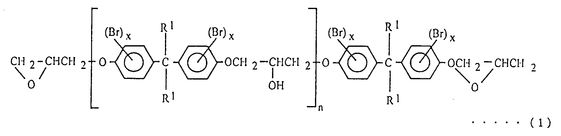
- For the cast epoxy resin composition, at least one kind of the brominated epoxy resins represented by the formula (1) which show a solid state at ordinary temperatures can be used as a mandatory component, and then added thereto may be epoxy resins which show a liquid state at ordinary temperatures, such as an epoxy resin with a bis A skeleton or a bis F skeleton, an alicyclic epoxy resin and an epoxy resin with a biphenyl skeleton. Further, it is possible to mix and use epoxy resins having various structures with the epoxy resins represented by the formula (1).
- There is no limit to the acid anhydride and acid anhydrides with various structures are usable. In addition, the acid anhydride may be used alone or in combinations thereof.
- The loading quantity of the acid anhydride to 100 parts by weight of epoxy is expressed as the formulae (2) to (4).

- In the formula (4), it is desirable that the value a is in a range of from 0.5 to 1.0. If the value a is out of this range, there is a possibility of great heating weight reduction taking place and the glass transition temperature decreasing to impair performance.
- Although when using a crosslinked rubber polymer powder with a functional group reactive to an epoxy resin adjustment according to the kind of functional group is required, the loading ratio in the reactive group between the principal epoxy group and the acid anhydride group must be in the aforesaid range.
- Examples of the crosslinked rubber powder include a hydrogenated butadiene rubber, a hydrogenated polyisoprene rubber, an acrylic rubber, a butadiene-acrylic rubber, or others, in a fine powder form with a particle diameter of from 0.01 to 50 µm. This fine powder is dispersed uniformly in the epoxy resin, with the result that the fracture toughness is improved and stress can be alleviated, thus reforming its crack resistance, productivity, formation property and so on. For achieving uniform mixing in a cure material, the crosslinked rubber power can be preliminary mixed with an epoxy resin or an acid anhydride.
- An appropriate loading quantity of the crosslinked rubber powder is from 5 to 30% by weight with respect to the total weight of the organic components. That is, a loading below 5% by weight fails to enhance the fracture toughness and makes it difficult to improve the crack resistance because the stress is barelly alleviated, while a loading above 30% by weight increases the viscosity of the composition to deteriorate the workability.
- Further, when an organic group (functional group) such as a carboxylic acid group, amino group and hydroxyl group reactive with an epoxy group exists on the particle surfaces of the crosslinked rubber powder, it reacts with an epoxy matrix during curing reaction to reinforce its interfaces, thereby enhancing its toughness.
- Although the functional group present on the rubber particles comes into reaction during the curing reaction, it may also be preliminarily reacted with the epoxy resin.
- As the inorganic filler, an alumina filler or a silica filler may be used. The alumina filler can be used singly or can be used together with the silica filler. In this instance, limitation is not imposed on their mixing ratio. Moreover, its configuration can assume a spherical shape or a broken form.
- Preferably, the average particle size of the inorganic fillers is below 60 µm, and in particular the average particle size is below 60 µm and more than 5% by weight of the fillers being particles having a size below 5 µm, and the content of the inorganic fillers is with in a range of from 10 to 80% by weight to the whole composition.
- On the other hand, the silica filler used in the present invention is a natural silica or a synthetic silica.
- Furthermore, as the hardening accelerator it is possible to use any kind of imidazole such as a 2-ethyl-4-methyl imidazole and their salts, phosphorus-based compounds represented by any kind of organic phosphine such as a liphenyl phosphine and a ring phosphine, aliphatic amines, aliphatic polyamines, aromatic amines, tertiary amines and their salts, dicyandiamides, any kind of Lewis acid and base catalyst, organic metallic salts such as salts of Brφnsted acids, zinc octylate and tin octylate, polymercaptans, microcapsule catalysts, and so on, which can serve as a hardening accelerator to cure the ordinary epoxy resin.
- These hardening accelerators may be used alone or in combination thereof. The quantity of the hardening accelerators to be used is from 0.05 to 10% by weight to 100% by weight of the epoxy resin.
- The aforesaid epoxy resin compositions can be mixed with a common mixing apparatus. Further, in the case of producing an insulating spacer using the aforesaid epoxy resin compositions, a common forming apparatus, for example a pressure gelation forming apparatus or the like, can be used without any limitations.
- Fig. 5 is an illustrative view of a structure of one example of a forming apparatus. In Fig. 5,
numerals tank 19, not including a curing accelerator, while designated atnumeral 38 is a curing accelerator reservoired in atank 17. Moreover, denoted atnumeral 39 is a metal pattern for an insulating spacer which accommodates a shield electrode (not shown) formed in advance and disposed. In this construction, theepoxy resin composition 37 and the curingaccelerator 38 separately reservoired are respectively fed throughcylinders mixer 25. Thismixer 25 quantitatively mixes theepoxy resin composition 37 and the curingaccelerator 38 and subsequently injects them under a pressure in a range of from 5 to 50 kg/cm2 into themetal pattern 39 heated up to from 100°C to 200°C, thereby achieving a high-speed formation. As mentioned above, the crack resistance of the insulating member (see Fig. 2) can be improved by blending the crosslinked rubber powder. - A detailed description will be made hereinbelow of the cast epoxy resin composition and the conductive epoxy resin composition according to embodiments of the present invention.
- With CT200 (WPE400, manufactured by Nagase Chiba Co., Ltd.) used as an epoxy resin, HN2200 (produced by Hitachi Kasei Kogyo Co., Ltd, neutralization equivalent : 83.0) as the acid anhydride, an alumina (A-42-6, produced by Showa Denko Co., Ltd., average particle diameter of 6.5 µm) as an inorganic filler and a zinc octylate as the curing accelerator, a mixture was made in a compounding or blending composition as shown in Table 1 to obtain a cast epoxy resin composition (a).
- In addition to the cast epoxy resin composition (a) of Example 7, carbon (produced by Kanebo Co., Ltd., Bellpearl C-800) was used as a conductive powder and mixed in the compounding composition shown in Table 1, thus attaining a conductive epoxy resin composition (b).

- With CT200 as the epoxy resin, HN2200 as the acid anhydride, a zinc octylate as the curing accelerator and an antimony oxide doped tin oxide SnO2 (T-1, produced by Mitsubishi Material Co., Ltd.) as the conductive powder, a mixture was made in the compounding composition shown in Table 1, thereby producing a conductive epoxy resin composition (c).
- With CT200 as the epoxy resin, HN2200 as the acid anhydride, and a nickel-coated phenol resin (Bellpearl N, produced by Kanebo Co., Ltd.) as the conductive powder, a mixture was made in the blending composition shown in Table 1 to produce a conductive epoxy resin composition (d).
- With CT200 as the epoxy resin, HN2200 as the acid anhydride, an alumina (A-42-6) as the inorganic filler, C-800 as the conductive powder and a zinc octylate as the curing accelerator, a mixture was made in a compounding or blending composition as shown in Table 1 to obtain a semi-conductive epoxy resin composition (e).
- With a brominated epoxy resin (E-5051, WPE650, Yuka Shell Epoxy Co., Ltd.) with a structure represented by a formula (5) shown below as the epoxy resin, HN2200 as the acid anhydride, an acrylonitrile-butadiene rubber (XER-91, produced by Japan Synthetic Rubber Co., Ltd.), which has a carboxylic acid group on its surface, as the crosslinked rubber, A-42-6 as the inorganic filler and a zinc octylate as the curing accelerator, a mixture was made in a compounding composition as shown in Table 2, thus providing a cast epoxy resin composition (f).


- In this example, a brominated epoxy resin (FBEP-13, WPE700, produced by Mitsui Toatsu Fine Co., Ltd.) which has a structure as represented by a formula (6) shown below was used as the epoxy resin and the other components were the same as those in Example 12. These components were mixed as shown in Table 2 to obtain a cast epoxy resin composition (g).

- In this Example, in place of the alumina filler (A-42-6) being the inorganic filler of the cast epoxy resin composition (f) in the above-mentioned Example 12, as shown in Table 2 the alumina filler (A-42-6) and a silica filler (RD-8, produced by Tatsumori Co., Ltd.) were blended and mixed therewith, thereby obtaining a cast epoxy resin (h).
- In this Example, in place of the alumina filler (A-42-6) being the inorganic filler of the cast epoxy resin composition (f) in the above-mentioned Example 12, as shown in Table 2 the silica filler (RD-8) was blended and mixed therewith, thereby obtaining a cast epoxy resin composition (i).
- In this Example, without using the alumina filler being the inorganic filler of the cast epoxy resin composition in the above-mentioned Example 12, as shown in Table 2 the conductive powder C-800 was blended and mixed to produce a conductive epoxy resin composition (j).
- The conductive powder C-800 was blended and mixed with the cast epoxy resin composition according to Example 12 as shown in Table 2, with the result that a semi-conductive epoxy resin composition (k) was produced.
- The cast epoxy resin composition (a) according to the aforesaid Example 7 was reservoired in the
tank 18 of the forming apparatus shown in Fig. 3, while the conductive epoxy resin composition (b) according to Example 8 was stored in thetank 19, and both the resin compositions (a) and (b) were kept at a temperature of 100°C. The respective resin compositions (a) and (b) were supplied through thecylinders mixer 25 with the mixture ratio (a/b) varying stepwise or continuously within a range of from more than 0/100 to 80/20. Themixer 25 mixed both the resin compositions (a) and (b) and subsequently injected them under a pressure of 30 kgf/mm2 into themetal pattern 28 kept at a temperature of 160°C. After curing within themetal pattern 28 for 12 hours, a conductive shield electrode ([1] in Table 3) was obtained which had a configuration as shown in Fig. 6. Fig. 6 is a front elevational view showing the conductive shield electrode ([1] in Table 3), and Fig. 7 is a cross-sectional view taken along a line VII-VII of Fig. 6. In Figs. 6 and 7, numeral 14 represents a connection fitting shown in Fig. 1.
- Fig. 8 is an illustrative view showing areas I, II and III in a cross section taken along a line VIII-VIII of Fig. 6.
- In Fig. 8, ash contents were measured through thermogravimetric analysis (TGA) on the cured materials in the respective areas I, II and III in order to confirm the mixture ratio of the inorganic filler. Further, the resistances in the respective areas I, II and III were obtained on the basis of the relationship between the mixture ratio of the inorganic filler (alumina filler) and the volumetric resistance experimentally given in advance as shown in Fig. 9. Table 3 shows the resultant volumetric resistances of shield electrodes.
- Subsequently, the obtained shield electrode [1] was placed within the metal pattern at a temperature of 160°C and cured with the cast epoxy resin composition (a) for 24 hours, thus producing an insulating spacer (A). Thereafter, ten cycles of a heat cycle test comprising a cycle of 100°C/one hour and 0°C/one hour were made to examine the presence or absence of crack occurrence, with the results being shown in Table 3. As shown in Table 3 the results of the measurements of the discharge start voltage of the shield electrode [1] of the insulating spacer (A) and the heat cycle test indicates that the discharge start voltage was sufficiently high and no cracks occurred.
- Using the cast epoxy resin composition (a) of Example 7 and the conductive epoxy resin composition (c) of Example 9, a conductive shield electrode [2] and an insulating spacer (B) as shown in Table 3 were manufactured in the same manner as described in Example 18.
- When a test for the insulating spacer (B) was done in the same way in Example 18, the result was such that as shown in Table 3 the discharge start voltage of the shield electrode [2] was satisfactorily high and no cracking took place.
- Using the cast epoxy resin composition (a) of Example 7 and the conductive epoxy resin composition (d) of Example 10, a conductive shield electrode [3] and an insulating spacer (C) as shown in Table 3 were produced in the same manner as described in Example 18.
- When a test of the insulating spacer (C) was made in the same way in Example 18, the result was such that as shown in Table 3 the discharge start voltage of the shield electrode [3] was satisfactorily high and no cracking took place.
- The cast epoxy resin composition (a) of Example 7 and the conductive epoxy resin composition (b) of Example 8 were mixed in such a way that their volumetric ratio a/b was 40/60 and then injected into the metal pattern heated to a temperature of 130°C, and cured for 24 hours in such a manner that the settling velocity varied due to the difference in specific gravity between the fillers, with the result that a conductive shield electrode [4] as shown in Table 3 was produced. Further, an insulating spacer (D) was obtained using the shield electrode [4] in the same manner as described in Example 18.
- A test of the obtained insulating spacer (D) was made in the same way as in Example 18. As shown in Table 3 the results were such that the discharge start voltage of the shield electrode [4] was sufficiently high and no cracking occurred.
- The semi-conductive epoxy resin composition (e) of Example 11 was injected into the metal pattern having a temperature of 130°C, and then cured for 24 hours, thus producing a semi-conductive shield electrode [5].
- Further, an insulating spacer (E) was obtained using the shield electrode [5] in the same manner as described in Example 18.
- A test of the obtained insulating spacer (E) was taken in the same way as in Example 18. The results were such that as shown in Table 3 the discharge start voltage of the shield electrode [5] was sufficiently high and no cracking occurred.
- Using the conductive epoxy resin composition (j) of Example 16 and the cast epoxy resin composition (f) of Example 12, a conductive shield electrode [6] was produced in the same manner as described in Example 18.
- Further, an insulating spacer (F), in which the shield electrode [6] was embedded, was obtained using the cast epoxy resin composition (a) in the same manner as described in Example 18.
- When a test of the insulating spacer (F) was made in the same manner in Example 18, the result was such that as shown in Table 3 the discharge start voltage of the shield electrode [6] was satisfactorily high and no cracking took place.
- The semi-conductive epoxy resin composition (k) of Example 17 was used to produce a shield electrode [7]. Subsequently, the shield electrode [7] was placed within the metal pattern with a temperature of 160°C and then cured with the cast epoxy resin composition (a) of Example 7 for 24 hours, thus obtaining an insulating spacer (G).
- When a test of the insulating spacer (G) was made in the same manner in Example 18, the result was such that as shown in Table 3 the discharge start voltage of the shield electrode [7] was satisfactorily high and no cracking took place.
- An aluminum (Al)-made shield electrode [8] was placed within a metal pattern with a temperature of 160°C and then cured with the cast epoxy resin composition (a) of Example 7 for 24 hours, thus obtaining an insulating spacer (Y).
- When a test of the insulating spacer (Y) was made in the same manner in Example 18, the result was such that as shown in Table 3 the discharge start voltage of the shield electrode [7] was considerably lower as compared with those of Examples 18-24 and the heat cycle test indicated the occurrence of cracks.
- The cast epoxy resin composition (a) of Example 7 and the conductive epoxy resin composition (b) of Example 8 were fed into the mixer 25 (see Fig. 3) in such a way that the mixture ratio (a/b) was varied stepwise or continuously out of a range of from more than 0/100 to 80/20 (below 0/100 and above 80/20) in contrast to Example 18. Thereafter, a shield electrode [9] and an insulating spacer (Z) were obtained in the same manner as described in Example 18.
- A test for the insulating spacer (Z) was made in the same way as in Example 18. In consequence, as shown in Table 3 the discharge start voltage of the shield electrode [9] was sufficiently high and no cracking occurred.
- The conductive shield electrode [1] of Example 18 was located within the metal pattern with a temperature of 160°C and then cured with the cast epoxy resin composition (f) of Example 12 for 24 hours, thus creating an insulating spacer (H).
- A test for the insulating spacer (H) was made in the same way as in Example 18. In consequence, as shown in Table 4 the discharge start voltage of the shield electrode [1] was sufficiently high and no cracking occurred.

- The conductive shield electrode [1] of Example 18 was located within the metal pattern with a temperature of 160°C and then cured with the cast epoxy resin composition (g) of Example 13 for 24 hours, thus creating an insulating spacer (I).
- A test for the insulating spacer (I) was made in the same way as in Example 18. In consequence, as shown in Table 4 the shield electrode [1] showed a sufficiently high discharge start voltage and no cracking occurred.
- The conductive shield electrode [1] of Example 18 was located within the metal pattern with a temperature of 160°C and then cured with the cast epoxy resin composition (h) of Example 14 for 24 hours, thus obtaining an insulating spacer (J).
- A test for the insulating spacer (J) was made in the same way as in Example 18. In consequence, as shown in Table 4 the shield electrode [1] indicated a sufficiently high discharge start voltage and no cracking occurred.
- The conductive shield electrode [1] of Example 18 was located within the metal pattern with a temperature of 160°C and then cured with the cast epoxy resin composition (i) of Example 15 for 24 hours, thus obtaining an insulating spacer (K).
- A test for the insulating spacer (K) was made in the same way as in Example 18. In consequence, as shown in Table 4 the shield electrode [1] showed a sufficiently high discharge start voltage and no cracking occurred.
- An aluminum (Al) shield electrode [10] was placed within a metal pattern with a temperature of 160°C and then cured with the cast epoxy resin composition (f) of Example 12 for 24 hours, thus obtaining an insulating spacer (L).
- A test for the insulating spacer (L) was made in the same way as in Example 18. In consequence, as shown in Table 4 the shield electrode [10] indicated a sufficiently high discharge start voltage and no cracking occurred.
- An aluminum (Al) shield electrode [10] was placed within a metal pattern with a temperature of 160°C and then cured with the cast epoxy resin composition (g) of Example 13 for 24 hours, thus obtaining an insulating spacer (M).
- A test for the insulating spacer (M) was made in the same way as in Example 18. In consequence, as shown in Table 4 the discharge start voltage of the shield electrode [10] was sufficiently high and no cracking occurred.
- An aluminum (Al) shield electrode [10] was placed within a metal pattern with a temperature of 160°C and then cured with the cast epoxy resin composition (h) of Example 14 for 24 hours, thus obtaining an insulating spacer (N).
- A test for the insulating spacer (N) was made in the same way as in Example 18. In consequence, as shown in Table 4 the discharge start voltage of the shield electrode [10] was sufficiently high and no cracking occurred.
- An aluminum (Al) shield electrode [10] was placed within a metal pattern with a temperature of 160°C and then cured with the cast epoxy resin composition (i) of Example 15 for 24 hours, thus obtaining an insulating spacer (P).
- A test for the insulating spacer (P) was made in the same way as in Example 18. In consequence, as shown in Table 4 the discharge start voltage of the shield electrode [10] was sufficiently high and no cracking occurred.
- An aluminum (Al) metallic member was coated with the conductive epoxy resin composition (j) of Example 16 to obtain a shield electrode (11). Further, the shield electrode [11] was placed within a metal pattern with a temperature of 160°C and then cured with the cast epoxy resin composition (a) of Example 7 for 24 hours, thereby producing an insulating spacer (Q).
- A test for the insulating spacer (Q) was made in the same way as in Example 18. In consequence, as shown in Table 4 the discharge start voltage of the shield electrode [11] was sufficiently high and no cracking occurred.
- The conductive shield electrode [6] of Example 23 was placed within a metal pattern with a temperature of 160°C and then cured with the cast epoxy resin composition (f) of Example 12 for 24 hours, thus obtaining an insulating spacer (R).
- A test for the insulating spacer (R) was made in the same way as in Example 18. In consequence, as shown in Table 4 the shield electrode [10] indicated a sufficiently high discharge start voltage and no cracking occurred.
- An aluminum (Al)-made shield electrode [10] was placed within a metal pattern with a temperature of 160°C and then cured with the cast epoxy resin composition (a) of Example 7 for 24 hours, thus obtaining an insulating spacer (Y).
- A test of the insulating spacer (Y) was made in the same way as in Example 18. Consequently, as shown in Table 4 the discharge start voltage of the shield electrode [10] was
less tahn 1/2 of those of Examples 25-34 and the result of the heat cycle test showed the occurrence of cracks. - An aluminum (Al) shield electrode [10] was placed within the
metal pattern 28 with a temperature of 160°C and further a conductive shield electrode [12] was obtained using the cast epoxy resins (a) and (b) used in Example 18 in the same forming manner as described in Example 18. Subsequently, the shield electrode [12] was cured with the cast epoxy resin (a) for 24 hours to obtain an insulating spacer (S). - A test for the insulating spacer (S) was made in the same way as in Example 18. In consequence, as shown in Table 5 the discharge start voltage of the shield electrode [12] was sufficiently high and no cracking occurred.

- A resin composition (e') which had the same composition as the semi-conductive epoxy resin (e) of Example 11 except that the amount of the curing accelerator was increased up to three parts by weight was used and injected into a metal pattern with a temperature of 160°C and then cured for 24 hours, thus producing a semi-conductive shield electrode [13]. Subsequently, the cast epoxy resin composition (a) of Example 7 was used and, after curing for 24 hours, an insulating spacer (T) was obtained.
- A test for the insulating spacer (T) was made in the same way as in Example 18. In consequence, as shown in Table 5 the shield electrode [13] showed a sufficiently high discharge start voltage and no cracking occurred.
- An aluminum (Al) shield electrode [10] was placed within the
metal pattern 28 with a temperature of 160°C and then cured with the cast epoxy resin (e') of Example 36 for 24 hours so that a semi-conductive shield electrode [14] was obtained. Subsequently, it was cured with the cast epoxy resin composition (a) of Example 7 for 24 hours, thereby producing an insulating spacer (U). - A test for the insulating spacer (U) was made in the same way as in Example 18. In consequence, as shown in Table 5 the shield electrode [14] showed a sufficiently high discharge start voltage and no cracking occurred.
- As obvious from the above-described Examples, the insulating spacers according to the present invention are constructed with a plastic made of an epoxy resin composition so that the volumetric specific resistance of the shield electrode increases toward the median point between the container and the conductor, and hence the concentration of electric fields in the boundary areas between the shield electrode and the insulating member is reducible with the result that reliability is improved, service life is lengthened and it is extremely useful in industrial fields.
- Moreover, the shield electrode manufacturing method according to the present invention can reduce the electric field concentration and hence produce a shield electrode which has high reliability and long service life and is extremely useful in industrial fields.
- Furthermore, in another insulating spacer according to the present invention, the insulating member is formed with a brominated epoxy resin composition comprising an epoxy resin, an acid anhydride curing agent, a crosslinked-rubber powder, an inorganic filler and a hardening accelerator. Accordingly, with the help of the contained crosslinked rubber powder, the glass transition temperature is increased and the thermal expansion coefficient is reduced, with the result that the crack resistance of the resultant insulating spacer improves to enhance its reliability and lengthen its service life so that its industrial value becomes extremely high.
- It should be understood that the foregoing relates only to preferred embodiments of the present invention, and that it is intended to cover all changes and modifications of the embodiments of the invention herein used for the purposes of the disclosure, which do not constitute departures from the spirit and scope of the invention.
Claims (9)
- An insulating spacer (16) comprising a conductor (6) placed in a grounded metallic container (2) packed with an insulating gas (1) and to which a high voltage is applied, an insulating member (11) for fixedly securing the conductor (6) to the container (2), and shield electrodes (12, 13) installed in the insulating member (11) in the vicinity of the container (2) and the conductor (6) or in the vicinity of the container (2), the shield electrodes (12, 13) being constructed with a plastic made of an epoxy resin composition so that their volumetric specific resistance increases toward the median point between the container (2) and the conductor (6).
- An insulating spacer (16) as defined in claim 1,
wherein the shield electrodes (12, 13) are made such that their volumetric specific resistance increases toward the median point between the container (2) and the conductor (6) within a range of from 100 to 1010 Ωcm. - An insulating spacer (16) as defined in claim 1 or 2,
wherein the shield electrodes (12) are constructed with the plastic made with the resin composition which is a mixture of an inorganic filler-filled epoxy resin composition (A, 18) and a conductive epoxy resin composition (B, 20). - An insulating spacer (16) as defined in claim 1 or 2,
wherein the shield electrodes (12, 13) are constructed with the plastic which is made with a conductive epoxy resin composition containing an inorganic filler (C) and a conductive powder (D) with a low specific gravity below 2.5. - An insulating spacer (16) comprising a conductor (6) placed in a grounded metallic container (2) packed with an insulating gas (1) and to which a high voltage is applied, an insulating member (11) for fixedly securing the conductor (6) to the container (2), and shield electrodes (12, 13) installed in the insulating member (11) in the vicinity of the container (2) and the conductor (6) or in the vicinity of the container (2), the shield elctrodes (12, 13) being constructed with a plastic made with a semi-conductive epoxy resin composition whose volumetric specific resistance is in a range of from 104 to 1010 Ωcm.
- An insulating spacer (16) as defined in any of claims 1 to 5,
wherein the shield electrodes (12, 13) are formed by coating a metallic member with the plastic. - An insulating spacer (16) comprising a conductor (6) placed in a grounded metallic container (2) packed with an insulating gas (1) and to which a high voltage is applied, an insulating member (11) for fixedly securing the conductor to the container, and shield electrodes (12, 13) installed in the insulating member (11) in the vicinity of the container (2) and the conductor (6) or in the vicinity of the container (2), the insulating member (11) being formed with an epoxy resin composition containing a brominated epoxy resin, an acid anhydride curing agent, a crosslinked-rubber powder, an inorganic filler and a hardening accelerator.
- A method of manufacturing shield electrodes (12, 13) of an insulating spacer (16) comprising a conductor (6) placed in a grounded metallic container (2) packed with an insulating gas (1) and to which a high voltage is applied, an insulating member (11) for fixedly securing the conductor (6) to the container (2), and shield electrodes (12, 13) installed in the insulating member (11) in the vicinity of the container (2) and the conductor (6) or in the vicinity of the container (2), wherein the shield electrodes (12, 13) are formed such that, an inorganic filler-filled epoxy resin composition (A, 18) and a conductive epoxy resin composition (B, 20) are injected into a molding metal pattern (28), with the mixed volumetric ratio (A/B) of the inorganic filler-filled epoxy resin composition (A) and the conductive epoxy resin composition (B) varying to increase within a range of from more than 0/100 to 80/20 toward the median point between the container (2) and the conductor (6), and cured.
- A method of manufacturing shield electrodes (12, 13) of an insulating spacer (16) comprising a conductor (6) placed in a grounded metallic container (2) packed with an insulating gas (1) and to which a high voltage is applied, an insulating member (11) for fixedly securing the conductor (6) to the container (2), and shield electrodes (12, 13) installed in the insulating member (11) in the vicinity of the container (2) and the conductor (6) or in the vicinity of the container (2), wherein the shield electrodes (12, 13) are formed such that, in injecting into a molding metal pattern and curing an epoxy resin composition containing an inorganic filler (C) and a conductive powder (D) with a low specific gravity below 2.5, volumetric specific resistance of the shield electrodes (12, 13) is made to vary to increase toward the median point between the container (2) and the conductor (6) using at least one of a centrifugal separating force and a difference in settling velocity between the inorganic filler (C) and the low specific gravity conductive powder (D) at curing.
Applications Claiming Priority (6)
| Application Number | Priority Date | Filing Date | Title |
|---|---|---|---|
| JP15772395 | 1995-06-23 | ||
| JP15772395 | 1995-06-23 | ||
| JP157723/95 | 1995-06-23 | ||
| JP10274396 | 1996-04-24 | ||
| JP102743/96 | 1996-04-24 | ||
| JP10274396A JP3588401B2 (en) | 1995-06-23 | 1996-04-24 | Manufacturing method of insulating spacer and shield electrode |
Publications (3)
| Publication Number | Publication Date |
|---|---|
| EP0750379A2 true EP0750379A2 (en) | 1996-12-27 |
| EP0750379A3 EP0750379A3 (en) | 1998-01-21 |
| EP0750379B1 EP0750379B1 (en) | 2002-05-29 |
Family
ID=26443420
Family Applications (1)
| Application Number | Title | Priority Date | Filing Date |
|---|---|---|---|
| EP96109994A Expired - Lifetime EP0750379B1 (en) | 1995-06-23 | 1996-06-20 | Insulating spacer |
Country Status (5)
| Country | Link |
|---|---|
| US (1) | US5723813A (en) |
| EP (1) | EP0750379B1 (en) |
| JP (1) | JP3588401B2 (en) |
| CN (1) | CN1049533C (en) |
| DE (1) | DE69621378T2 (en) |
Cited By (4)
| Publication number | Priority date | Publication date | Assignee | Title |
|---|---|---|---|---|
| DE19621710A1 (en) * | 1996-05-30 | 1997-12-04 | Abb Research Ltd | Insulator for high voltage switchgear |
| EP0899844A1 (en) * | 1997-08-29 | 1999-03-03 | Asea Brown Boveri AG | Gas insulated conductor and method for manufacturing it |
| EP3142205A1 (en) * | 2015-09-11 | 2017-03-15 | ABB Schweiz AG | High dc voltage insulator, high voltage unit for direct current with high dc voltage insulator and their use |
| DE102016214408A1 (en) * | 2016-08-04 | 2018-02-08 | Siemens Aktiengesellschaft | insulator |
Families Citing this family (14)
| Publication number | Priority date | Publication date | Assignee | Title |
|---|---|---|---|---|
| DE10339822A1 (en) * | 2003-08-25 | 2005-04-14 | Siemens Ag | Gas-insulated high-voltage system |
| JP4673690B2 (en) * | 2005-07-15 | 2011-04-20 | 株式会社東芝 | Injection device for pressure gelation |
| JP5072256B2 (en) * | 2006-04-21 | 2012-11-14 | 株式会社東芝 | Insulating spacer, manufacturing method thereof, and gas insulating switchgear using the same |
| DE102007056147A1 (en) * | 2007-11-16 | 2009-05-20 | Siemens Ag | Arrangement with an insulating body and method for producing an insulating material |
| JP5414290B2 (en) * | 2009-01-28 | 2014-02-12 | 株式会社東芝 | Casting device, casting method and insulating spacer |
| JP5461260B2 (en) * | 2010-03-19 | 2014-04-02 | 株式会社日立製作所 | Insulated spacer with built-in optical fiber |
| US8502159B2 (en) * | 2010-04-29 | 2013-08-06 | Battelle Energy Alliance, Llc | Apparatuses and methods for generating electric fields |
| US20110266436A1 (en) * | 2010-04-29 | 2011-11-03 | Battelle Energy Alliance, Llc | Apparatuses and methods for forming electromagnetic fields |
| JP4781493B1 (en) * | 2011-02-28 | 2011-09-28 | 三菱電機株式会社 | Gas insulated bus |
| WO2013030388A1 (en) * | 2011-09-02 | 2013-03-07 | Abb Research Ltd | Insulator for high-voltage gas insulated switch gear |
| CN104051084A (en) * | 2013-03-15 | 2014-09-17 | 西门子公司 | Disassemble insulator for gas insulated switchgear |
| CN103986114B (en) * | 2014-03-31 | 2017-01-11 | 国网江苏省电力公司盐城供电公司 | Gas-insulated device |
| DE102019134463B3 (en) * | 2019-12-16 | 2021-05-12 | TRUMPF Hüttinger GmbH + Co. KG | High frequency high voltage electrical conductor device |
| KR102808898B1 (en) * | 2023-05-24 | 2025-05-19 | 에이치디현대일렉트릭 주식회사 | Spacer with insulation shield ring between tanks, and gas insulated switchgear using the same |
Family Cites Families (32)
| Publication number | Priority date | Publication date | Assignee | Title |
|---|---|---|---|---|
| US3317659A (en) * | 1965-09-22 | 1967-05-02 | Gen Electric | High voltage insulator with internal corona shield |
| US3617606A (en) * | 1970-06-19 | 1971-11-02 | Gen Electric | Shielded bushing construction |
| US3673305A (en) * | 1970-11-04 | 1972-06-27 | Detroit Edison Co | Capacitively graded modular pothead for h-v cable |
| US3801725A (en) * | 1972-11-14 | 1974-04-02 | Westinghouse Electric Corp | Spacer construction for fluid-insulated transmission lines |
| FR2319183A1 (en) * | 1975-07-22 | 1977-02-18 | Comp Generale Electricite | DEVICE FOR MAINTAINING THE GAP BETWEEN TWO ELECTRIC CONDUCTORS |
| US4038491A (en) * | 1976-03-30 | 1977-07-26 | Westinghouse Electric Corporation | Fluid casting composition containing low expansion glass filler |
| DE2726291A1 (en) * | 1977-06-10 | 1978-12-21 | Kabel Metallwerke Ghh | Multilayer high voltage power cable - built up of central conductor, laminated foam insulation conductive tape envelope and strong corrugated mantle |
| JPS5678315A (en) * | 1979-11-29 | 1981-06-27 | Toshiba Chem Prod | Insulating spacer |
| JPS5728516A (en) * | 1980-07-29 | 1982-02-16 | Toshiba Chem Prod | Supporting spacer |
| JPS5795110A (en) * | 1980-11-29 | 1982-06-12 | Tokyo Shibaura Electric Co | Insulating spacer |
| JPS5828523U (en) * | 1981-08-18 | 1983-02-24 | 株式会社東芝 | Conductor support device |
| JPS59166524A (en) * | 1983-03-14 | 1984-09-19 | Yuka Shell Epoxy Kk | Brominated epoxy resin composition |
| JPS6044519A (en) * | 1983-08-23 | 1985-03-09 | Showa Denko Kk | Epoxy resin composition for electrical circuit casting |
| EP0148394B2 (en) * | 1983-11-30 | 1994-08-03 | Kabushiki Kaisha Toshiba | Enclosed switchgears |
| JPS61180541U (en) * | 1985-04-25 | 1986-11-11 | ||
| JPS6258820A (en) * | 1985-09-05 | 1987-03-14 | 株式会社東芝 | insulation spacer |
| JPS62166719A (en) * | 1986-01-20 | 1987-07-23 | 株式会社東芝 | Insulating spacer |
| JPS6311014A (en) * | 1986-06-30 | 1988-01-18 | 株式会社東芝 | Insulating spacer |
| JPS6328214A (en) * | 1986-07-18 | 1988-02-05 | 株式会社東芝 | Insulating spacer |
| JPH0677932B2 (en) * | 1986-12-09 | 1994-10-05 | 古河電気工業株式会社 | Epoxy resin cast product manufacturing method |
| JPH0828930B2 (en) * | 1987-02-13 | 1996-03-21 | 株式会社東芝 | Corn type insulation spacer |
| JPS63242113A (en) * | 1987-03-30 | 1988-10-07 | 株式会社東芝 | Insulating spacer |
| JPH0613565Y2 (en) * | 1987-10-16 | 1994-04-06 | 日東電工株式会社 | Conductor support device |
| JPH0528894Y2 (en) * | 1987-11-05 | 1993-07-26 | ||
| DE4007335A1 (en) * | 1990-03-08 | 1991-09-12 | Asea Brown Boveri | Electrical insulator sepg. inner from grounded outer conductors - comprises plastic cpd. with inert filler and has embedded ring shaped regions with higher dielectric constant to modify field |
| DE4015929A1 (en) * | 1990-05-17 | 1991-11-21 | Asea Brown Boveri | Gas insulated HV installation isolator - has at least one field control element of electrically conductive plastic coupled by moulding onto insulator body |
| JPH04210715A (en) * | 1990-11-30 | 1992-07-31 | Mitsubishi Cable Ind Ltd | Connecting method for rubber/plastic power cable |
| JPH0522830A (en) * | 1991-07-12 | 1993-01-29 | Toshiba Corp | Insulation spacer |
| JPH0581952A (en) * | 1991-09-24 | 1993-04-02 | Toshiba Corp | Insulation spacer |
| JPH05242733A (en) * | 1992-02-25 | 1993-09-21 | Hitachi Cable Ltd | Electrically insulating material |
| US5589129A (en) * | 1993-02-19 | 1996-12-31 | Kabushiki Kaisha Toshiba | Method of manufacturing a molding using a filler or an additive concentrated on an arbitrary portion or distributed at a gradient concentration |
| DE19500849A1 (en) * | 1995-01-13 | 1996-07-18 | Abb Research Ltd | Electrical component |
-
1996
- 1996-04-24 JP JP10274396A patent/JP3588401B2/en not_active Expired - Fee Related
- 1996-06-14 US US08/663,733 patent/US5723813A/en not_active Expired - Lifetime
- 1996-06-20 EP EP96109994A patent/EP0750379B1/en not_active Expired - Lifetime
- 1996-06-20 CN CN96100588A patent/CN1049533C/en not_active Expired - Fee Related
- 1996-06-20 DE DE69621378T patent/DE69621378T2/en not_active Expired - Lifetime
Cited By (6)
| Publication number | Priority date | Publication date | Assignee | Title |
|---|---|---|---|---|
| DE19621710A1 (en) * | 1996-05-30 | 1997-12-04 | Abb Research Ltd | Insulator for high voltage switchgear |
| EP0899844A1 (en) * | 1997-08-29 | 1999-03-03 | Asea Brown Boveri AG | Gas insulated conductor and method for manufacturing it |
| EP3142205A1 (en) * | 2015-09-11 | 2017-03-15 | ABB Schweiz AG | High dc voltage insulator, high voltage unit for direct current with high dc voltage insulator and their use |
| WO2017042197A1 (en) * | 2015-09-11 | 2017-03-16 | Abb Schweiz Ag | Dc voltage high-voltage insulator, high-voltage system for direct current with dc voltage high-voltage insulator, and use thereof |
| CN108352696A (en) * | 2015-09-11 | 2018-07-31 | Abb瑞士股份有限公司 | DC voltage high-tension insulator, with DC voltage high-tension insulator for the high pressure facility of DC current and its application |
| DE102016214408A1 (en) * | 2016-08-04 | 2018-02-08 | Siemens Aktiengesellschaft | insulator |
Also Published As
| Publication number | Publication date |
|---|---|
| JP3588401B2 (en) | 2004-11-10 |
| CN1139306A (en) | 1997-01-01 |
| CN1049533C (en) | 2000-02-16 |
| DE69621378D1 (en) | 2002-07-04 |
| JPH0970126A (en) | 1997-03-11 |
| EP0750379B1 (en) | 2002-05-29 |
| US5723813A (en) | 1998-03-03 |
| DE69621378T2 (en) | 2003-01-23 |
| EP0750379A3 (en) | 1998-01-21 |
Similar Documents
| Publication | Publication Date | Title |
|---|---|---|
| US5723813A (en) | Insulating spacer with shield electrodes having a graded resistance | |
| EP1176171B1 (en) | Electric insulating material and method of manufacture thereof | |
| EP2198433B1 (en) | Polymer concrete electrical insulation system | |
| EP1342025B1 (en) | Form-in-place gasket for electronic applications | |
| US11059936B2 (en) | Organofluorine modified epoxy resins for increasing surface flashover voltage, and preparation methods and applications thereof | |
| EP2264102A1 (en) | Cast insulation resin for electric apparatus and high voltage electric apparatus using the same | |
| EP2230267A1 (en) | Curable Epoxy Resin Composition | |
| EP2982721B1 (en) | Coating material for electrical equipment, method for manufacturing coating material for electrical equipment, and encapsulated type insulating device | |
| CN110218414A (en) | A kind of composition epoxy resin and its preparation method and application | |
| CN111944388A (en) | Insulating powder coating for coating surface of connecting copper bar and preparation method thereof | |
| EP0676448B1 (en) | Epoxy resin composition and resin molding using the same | |
| EP0174510A2 (en) | Epoxy resin composition for encapsulation of semiconductor device | |
| JPH07109337A (en) | Epoxy resin casting material | |
| CN102181128A (en) | Epoxy resin premix and preparation technology of the epoxy resin premix | |
| KR20090037355A (en) | Resin composition for fuel cell separator and separator for fuel cell | |
| CN111363315B (en) | Epoxy resin insulating material and preparation method and application thereof | |
| JPH1060085A (en) | Resin composition for molding, molded product for high voltage equipment by using the same and its production | |
| EP1387860B1 (en) | Moulding composition for producing bipolar plates | |
| CN1160063A (en) | Epoxy resin composition and insulating spacer | |
| EP0160829A1 (en) | Epoxy resin composition for cast molding | |
| CN104845375A (en) | Low-dielectric-constant liquid silicone rubber composite material and preparation method thereof | |
| JP2001135144A (en) | Cast product for SF6 gas insulated equipment and method of manufacturing the same | |
| JP2000086744A (en) | Epoxy resin composition, inductance component and semiconductor sealing device | |
| JP2004063326A (en) | High frequency components | |
| JPH1160912A (en) | Casting resin composition and insulating spacer comprising this resin composition |
Legal Events
| Date | Code | Title | Description |
|---|---|---|---|
| PUAI | Public reference made under article 153(3) epc to a published international application that has entered the european phase |
Free format text: ORIGINAL CODE: 0009012 |
|
| AK | Designated contracting states |
Kind code of ref document: A2 Designated state(s): CH DE FR LI |
|
| PUAL | Search report despatched |
Free format text: ORIGINAL CODE: 0009013 |
|
| AK | Designated contracting states |
Kind code of ref document: A3 Designated state(s): CH DE FR LI |
|
| 17P | Request for examination filed |
Effective date: 19980128 |
|
| 17Q | First examination report despatched |
Effective date: 19981208 |
|
| RTI1 | Title (correction) |
Free format text: INSULATING SPACER |
|
| GRAG | Despatch of communication of intention to grant |
Free format text: ORIGINAL CODE: EPIDOS AGRA |
|
| GRAG | Despatch of communication of intention to grant |
Free format text: ORIGINAL CODE: EPIDOS AGRA |
|
| GRAH | Despatch of communication of intention to grant a patent |
Free format text: ORIGINAL CODE: EPIDOS IGRA |
|
| GRAH | Despatch of communication of intention to grant a patent |
Free format text: ORIGINAL CODE: EPIDOS IGRA |
|
| GRAH | Despatch of communication of intention to grant a patent |
Free format text: ORIGINAL CODE: EPIDOS IGRA |
|
| GRAA | (expected) grant |
Free format text: ORIGINAL CODE: 0009210 |
|
| AK | Designated contracting states |
Kind code of ref document: B1 Designated state(s): CH DE FR LI |
|
| REG | Reference to a national code |
Ref country code: CH Ref legal event code: NV Representative=s name: WILLIAM BLANC & CIE CONSEILS EN PROPRIETE INDUSTRI Ref country code: CH Ref legal event code: EP |
|
| REF | Corresponds to: |
Ref document number: 69621378 Country of ref document: DE Date of ref document: 20020704 |
|
| ET | Fr: translation filed | ||
| PLBE | No opposition filed within time limit |
Free format text: ORIGINAL CODE: 0009261 |
|
| STAA | Information on the status of an ep patent application or granted ep patent |
Free format text: STATUS: NO OPPOSITION FILED WITHIN TIME LIMIT |
|
| 26N | No opposition filed |
Effective date: 20030303 |
|
| REG | Reference to a national code |
Ref country code: CH Ref legal event code: PFA Owner name: MITSUBISHI DENKI KABUSHIKI KAISHA Free format text: MITSUBISHI DENKI KABUSHIKI KAISHA#2-3, MARUNOUCHI 2-CHOME CHIYODA-KU#TOKYO 100 (JP) -TRANSFER TO- MITSUBISHI DENKI KABUSHIKI KAISHA#2-3, MARUNOUCHI 2-CHOME CHIYODA-KU#TOKYO 100 (JP) |
|
| PGFP | Annual fee paid to national office [announced via postgrant information from national office to epo] |
Ref country code: DE Payment date: 20100616 Year of fee payment: 15 |
|
| REG | Reference to a national code |
Ref country code: CH Ref legal event code: PCAR Free format text: NOVAGRAAF SWITZERLAND SA;CHEMIN DE L'ECHO 3;1213 ONEX (CH) |
|
| PGFP | Annual fee paid to national office [announced via postgrant information from national office to epo] |
Ref country code: CH Payment date: 20110614 Year of fee payment: 16 Ref country code: FR Payment date: 20110621 Year of fee payment: 16 |
|
| REG | Reference to a national code |
Ref country code: DE Ref legal event code: R084 Ref document number: 69621378 Country of ref document: DE Effective date: 20110506 Ref country code: DE Ref legal event code: R084 Ref document number: 69621378 Country of ref document: DE Effective date: 20110704 |
|
| REG | Reference to a national code |
Ref country code: CH Ref legal event code: PL |
|
| REG | Reference to a national code |
Ref country code: CH Ref legal event code: PL |
|
| REG | Reference to a national code |
Ref country code: FR Ref legal event code: ST Effective date: 20130228 |
|
| REG | Reference to a national code |
Ref country code: DE Ref legal event code: R119 Ref document number: 69621378 Country of ref document: DE Effective date: 20130101 |
|
| PG25 | Lapsed in a contracting state [announced via postgrant information from national office to epo] |
Ref country code: CH Free format text: LAPSE BECAUSE OF NON-PAYMENT OF DUE FEES Effective date: 20120630 Ref country code: FR Free format text: LAPSE BECAUSE OF NON-PAYMENT OF DUE FEES Effective date: 20120702 Ref country code: DE Free format text: LAPSE BECAUSE OF NON-PAYMENT OF DUE FEES Effective date: 20130101 Ref country code: LI Free format text: LAPSE BECAUSE OF NON-PAYMENT OF DUE FEES Effective date: 20120630 |