EP0745909B1 - In-line color electrophotographic printer - Google Patents
In-line color electrophotographic printer Download PDFInfo
- Publication number
- EP0745909B1 EP0745909B1 EP96106852A EP96106852A EP0745909B1 EP 0745909 B1 EP0745909 B1 EP 0745909B1 EP 96106852 A EP96106852 A EP 96106852A EP 96106852 A EP96106852 A EP 96106852A EP 0745909 B1 EP0745909 B1 EP 0745909B1
- Authority
- EP
- European Patent Office
- Prior art keywords
- photoreceptor
- developer
- toner
- layer
- web
- Prior art date
- Legal status (The legal status is an assumption and is not a legal conclusion. Google has not performed a legal analysis and makes no representation as to the accuracy of the status listed.)
- Expired - Lifetime
Links
Images

Classifications
-
- G—PHYSICS
- G03—PHOTOGRAPHY; CINEMATOGRAPHY; ANALOGOUS TECHNIQUES USING WAVES OTHER THAN OPTICAL WAVES; ELECTROGRAPHY; HOLOGRAPHY
- G03G—ELECTROGRAPHY; ELECTROPHOTOGRAPHY; MAGNETOGRAPHY
- G03G15/00—Apparatus for electrographic processes using a charge pattern
- G03G15/01—Apparatus for electrographic processes using a charge pattern for producing multicoloured copies
- G03G15/0142—Structure of complete machines
- G03G15/0147—Structure of complete machines using a single reusable electrographic recording member
- G03G15/0152—Structure of complete machines using a single reusable electrographic recording member onto which the monocolour toner images are superposed before common transfer from the recording member
- G03G15/0157—Structure of complete machines using a single reusable electrographic recording member onto which the monocolour toner images are superposed before common transfer from the recording member with special treatment between monocolour image formation
-
- G—PHYSICS
- G03—PHOTOGRAPHY; CINEMATOGRAPHY; ANALOGOUS TECHNIQUES USING WAVES OTHER THAN OPTICAL WAVES; ELECTROGRAPHY; HOLOGRAPHY
- G03G—ELECTROGRAPHY; ELECTROPHOTOGRAPHY; MAGNETOGRAPHY
- G03G15/00—Apparatus for electrographic processes using a charge pattern
- G03G15/01—Apparatus for electrographic processes using a charge pattern for producing multicoloured copies
- G03G15/0142—Structure of complete machines
- G03G15/0147—Structure of complete machines using a single reusable electrographic recording member
- G03G15/0152—Structure of complete machines using a single reusable electrographic recording member onto which the monocolour toner images are superposed before common transfer from the recording member
- G03G15/0168—Structure of complete machines using a single reusable electrographic recording member onto which the monocolour toner images are superposed before common transfer from the recording member single rotation of recording member to produce multicoloured copy
-
- G—PHYSICS
- G03—PHOTOGRAPHY; CINEMATOGRAPHY; ANALOGOUS TECHNIQUES USING WAVES OTHER THAN OPTICAL WAVES; ELECTROGRAPHY; HOLOGRAPHY
- G03G—ELECTROGRAPHY; ELECTROPHOTOGRAPHY; MAGNETOGRAPHY
- G03G2215/00—Apparatus for electrophotographic processes
- G03G2215/01—Apparatus for electrophotographic processes for producing multicoloured copies
- G03G2215/0167—Apparatus for electrophotographic processes for producing multicoloured copies single electrographic recording member
- G03G2215/017—Apparatus for electrophotographic processes for producing multicoloured copies single electrographic recording member single rotation of recording member to produce multicoloured copy
-
- G—PHYSICS
- G03—PHOTOGRAPHY; CINEMATOGRAPHY; ANALOGOUS TECHNIQUES USING WAVES OTHER THAN OPTICAL WAVES; ELECTROGRAPHY; HOLOGRAPHY
- G03G—ELECTROGRAPHY; ELECTROPHOTOGRAPHY; MAGNETOGRAPHY
- G03G2215/00—Apparatus for electrophotographic processes
- G03G2215/02—Arrangements for laying down a uniform charge
- G03G2215/021—Arrangements for laying down a uniform charge by contact, friction or induction
-
- G—PHYSICS
- G03—PHOTOGRAPHY; CINEMATOGRAPHY; ANALOGOUS TECHNIQUES USING WAVES OTHER THAN OPTICAL WAVES; ELECTROGRAPHY; HOLOGRAPHY
- G03G—ELECTROGRAPHY; ELECTROPHOTOGRAPHY; MAGNETOGRAPHY
- G03G2215/00—Apparatus for electrophotographic processes
- G03G2215/04—Arrangements for exposing and producing an image
- G03G2215/0497—Exposure from behind the image carrying surface
Definitions
- This invention relates to color electrophotographic printers and, more particularly, to single pass color EP printers exhibiting improved performance characteristics.
- the prior art includes many teachings of full color electrophotographic (EP) printer configurations.
- Many color EP printers employ a four-pass configuration wherein four developer modules are arrayed along a photoreceptor surface.
- the developer modules are allocated to the deposition of cyan, yellow, magenta, and black toners onto the moving photoreceptor surface.
- a charging station uniformly sensitizes the photoreceptor surface.
- An exposure station selectively discharges the photoreceptor surface in accordance with respective color plane image data.
- the photoreceptor surface is then passed over the developer modules, with one developer module being brought into engagement with the photoreceptor surface to allow development of one color of the exposed image.
- U.S. Patent 5,300,990 to Thompson illustrates a liquid EP printer developer module and further describes (see Fig. 3) that such developer modules can be positioned side-by-side beneath a web-photoreceptor.
- the Thompson patent does not disclose whether the liquid EP system is single pass or four pass. Once the image in the Thompson system is fully developed on the photoreceptor surface, it is transferred to a sheet of paper or to an intermediate transfer medium.
- U.S. Patent 5,016,062 to Rapkin discloses a multicolor EP printer which includes four secondary imaging drums that are positioned along the path of an endless web. In accordance with the multi-color image to be produced, each drum is appropriately exposed in accordance with data from a single color plane and a paper sheet is passed in contact therewith via the endless web to enable toner transfer. After the sheet has contacted all of the secondary imaging drums, it contains a full color image.
- U.S. Patent 4,905,047 to Ariyama employs a liquid toner to achieve the imaging of the respective secondary drums.
- U.S. Patent 4,788,574 to Matsumoto et al. also discloses a four-drum/conveyor belt developer system for an in-line color printer.
- European Patent 0 599 296 to Fukuchi et al. illustrates a single pass color copier which includes a four plane memory for storing yellow, magenta, cyan and black pixel data.
- Fukuchi et al. use a web photoreceptor having a plurality of liquid toner developer modules arrayed along one surface. Between each developer module, a laser beam images the web photoreceptor in accordance with a particular color plane's pixel data. Immediately after each imaging action, a development occurs in accordance with the charge states on the web photoreceptor.
- the web photoreceptor is again charged and developed in accordance with a next color plane's image data.
- the procedure continues until all four image planes have been exposed and developed, at which point the image is transferred to a paper sheet.
- Fukuchi et al. employ powder toners to achieve their individual color toning actions.
- U.S. Patent 4,599,285 to Haneda et al. discloses an EP apparatus wherein plural developers are positioned along a photoreceptor web, with each developer module employing a two-component powder toner. Electrostatic recording heads are positioned between the individual developer modules to allow a writing of pixel charge states on the photoreceptor web in accordance with particular color plane data.
- US-A-5,241,356 discloses a multi-color imaging apparatus.
- This multi-color imaging apparatus basically uses two different development approaches, namely the so-called “CAD approach” (charged area development) and the “DAD approach” (discharged area development).
- CAD charged area development
- DAD discharged area development
- a so-called "post CAD” erase lamp 34 is provided, which serves to reduce the charge level of the photoreceptor in the toned or developed areas.
- US-A-5,272,508 concerns an electrophotographic photosensitive member and is basically concerned with the specific structure of a drum-shaped or endless-shaped light transmissive carrier used in electrophotographic printing.
- EP-A-0 398 592 discloses the use of thin film electroluminescent edge emitters in electrophotographic printing. However, the printer does not provide four erase means inbetween respective development modules, as is taught by the present invention.
- JP-A-02 106367 relates to a color printer using a photo-receptor web which passes past a number of developer stations wherein, prior to each developer station, a uniform charger and a writing charger is provided. For providing the necessary erasure of the photoreceptor web, one erase means is arranged prior to the four developer stations.
- a single pass full color EP printer exhibiting an improved architecture and speed of operation is provided. Further, an improved full color EP printer is provided that employs liquid toner developer modules, but avoids drip lines on the photoreceptor. Moreover, an improved full color EP printer is provided wherein mechanisms to engage and disengage developer modules are avoided.
- a single pass EP color printer includes a photoreceptor web having multiple layers and including a charge transport layer and a charge generation layer.
- Four exposure devices e.g. either laser-based or thin film electroluminescent edge emitting (TFEL) devices
- TFEL thin film electroluminescent edge emitting
- a liquid toner developer module is associated with each exposure device and includes a liquid toner reservoir, a developer roll for carrying the liquid toner to a transfer point and a squeegee roll.
- Each developer module is fixed so as to position its developer roll at a constant prescribed distance from the photoreceptor web at the toner transfer point and to create a fluid interfacial layer between its developer roll and the photoreceptor web.
- each squeegee roll is maintained in constant contact with the photoreceptor web.
- Erasure devices and corona charging devices are positioned between the respective developer modules to enable preparation of the photoreceptor web for a subsequent exposure/development operation.
- a drying roll is positioned after a last developer module for fixing the imaged toner on the photoreceptor web.
- the exposure devices operate from either the lower side of the photoreceptor web or from the upper side; however, in the latter instance, the photoreceptor web is comprised of a transparent support and ground plane layer.
- Fig. 1 illustrates a schematic representation of a single-pass, liquid toner, multi-color, EP printer 10 incorporating the invention.
- a photoreceptor web 12 is positioned over drive roller 14 and follower rollers 16 and 18. Photoreceptor web 12 is further engaged by four separate developer stations, each developer station being structurally identical but applying a different color liquid toner to photoreceptor web 12.
- Each developer station e.g. 20
- Each developer station includes an erase head 22, a corona charge module 24, a scanning laser write head 26, a developer module 28 and a liquid toner reservoir 30.
- Reservoir 30, in the example shown in Fig. 1, contains a cyan liquid toner including both a toner component and a dispersant component (e.g.
- developer stations 32, 34, and 36 are arrayed linearly along photoreceptor web 12 and provide exposure and developing functions for magenta, yellow and black toners. Developer station 20 will be hereafter described in detail, but it is to be understood that each of developer stations 32, 34 and 36 is substantially identical and performs similar functions.
- EP printer 10 includes a processor and a resident memory, which includes memory planes reserved for pixel data representing cyan, magenta, yellow and black pixel data that is to printed.
- data resident in the processor's memory that is representative of cyan pixel data is fed (in signal form) to laser 26 which is, in turn, scanned across photoreceptor web 12 to create corresponding pixel charge states thereon.
- an erase head 22 Prior to the scan action, an erase head 22 is operated to discharge photoreceptor web 12.
- Erase head 22 preferably comprises a light source that spans the width of photoreceptor web 12 and causes an erasure of previously written pixel data.
- a corona charge module 24 which causes photoreceptor web 12 to achieve a uniform charge state across its width.
- corona charge module 24 After corona charge module 24 has charged photoreceptor web 12 to a uniform charge state, laser module 26 is scanned to write a cyan pixel image across the width of photoreceptor web 12. Thereafter, the image-containing portion of photoreceptor web 12 is moved through developer module 28 which, in this preferred embodiment, is in continual engagement with photoreceptor web 12. Developer module 28 is supplied with cyan liquid toner from liquid toner reservoir 30. Developer roll 38 receives the cyan liquid toner and entrains that toner around its outer periphery to a transfer point 39. As shown in Fig.
- developer roll 38 is not in physical contact with photoreceptor web 12 but is spaced therefrom by a prescribed distance so as to create a fluid interfacial layer at transfer point 39 so as to enable migration of toner particles in the liquid toner to the appropriately discharged areas on photoreceptor web 12.
- the distance between photoreceptor web 12 and developer roll 38 is assured by proper adjustment of a cam 40.
- a squeegee roll 42 which rotates in a direction coincident with the direction of movement of photoreceptor web 12. Squeegee roll 42 enables the removal of a substantial percentage of the solvent from the toner present on photoreceptor web 12 and enables the cyan-toned image to emerge from developer module 28 in a substantially dry state. In fact, it has been found that the exiting cyan-toned image is sufficiently dry, given proper adjustment of developer module 28, to enable an immediate subsequent toning by a further liquid toner.
- toner module 28 Excess liquid toner from the toning and squeegee actions in toner module 28 is captured by an enclosure 44 and is returned to liquid toner reservoir 30 for reuse.
- Each of the developer modules in developer stations 20, 32, 34, and 36 remains in constant engagement with photoreceptor web 12. As a result, no load variations occur on photoreceptor web 12 due to engagement and disengagement of the respective developer modules. Further, no drip line is created by disengagement of a developer module from photoreceptor web 12.
- each of developer stations 20, 32, 34 and 36 is functionally equivalent except that each is responsive to data from a different color plane within the memory of printer 10.
- the toned image is moved to developer station 32 where photoreceptor web 12 is charged and exposed in accord with magenta pixel data and is then appropriately toned with magenta toner.
- the cyan/magenta toned image is moved to developer stations 34 and 36 where the image receives both yellow and black image data and toning.
- the fully toned image passes beneath drying roll 46 (which is heated and applies pressure) and then passes to an intermediate transfer roller 48 where the image is transferred to a sheet 50.
- Sheet 50 as is known in the art, is fed from a paper tray 52 under control of a rotatable cam 54 and feed rollers 56, 58, etc.
- a substrate/ground plane 60 forms a support layer and has arrayed on it a charge transport layer 62, a charge generation layer 64 and a release/overcoat layer 66.
- Charge generation layer 64 responds to incident laser light to generate corresponding charge pairs.
- Charge transport layer 62 provides a charge travel path which allows migration of certain charges states to ground plane 60 while other charge states migrate to the interface between charge generation layer 64 and release/overcoat layer 66. Because charge generation layer 64 is very close to the surface of photoreceptor belt 12 and is extremely thin, its speed of photo response is excellent.
- charge generation layer 64 0.1 ⁇ m
- charge transport layer 62 15 ⁇ m
- a preferred material for the charge generation layer is a metal-free phthalocyanine.
- the charge transport layer is comprised of charge transport molecules dispersed in an inert binder. Further details regarding a photoreceptor such as shown in Fig. 2 can be found in Organic Photoconductors For Imaging System, Borsenberger et al., Published by M. Dekker Inc., New York (1993).
- each of developer stations 20', 32', 34', and 36' is structurally identical to that shown in Fig. 1, except that each developer station now includes a drying roll 70 and a mating roll 72.
- the inclusion of a drying roll 70 with each developer station increases the overall length and complexity of the printer structure but provides further assurance that a dry toned surface will enter a subsequent developer station.
- Mating rolls 72 assure that belt 12 is pressed against drying roll 70 with sufficient pressure so that the toner present on photoreceptor web 12 is fixed by a combination of the pressure and heat applied via drying roll 70.
- the EP printers shown in Fig. 1 and Fig. 4 employ scanning laser modules 26 to achieve desired pixel charge states on photoreceptor web 12. Since a single pass color printer requires a subsequent color plane image to be precisely registered with a previously toned color image, it is critical that the placement of laser modules 26 be precisely controlled. Further, laser scanners exhibit errors of scale, bow, linearity and intensity that need to be matched and adjusted. Additionally, laser scanners are subject to vibration and other environmental effects which may cause registration problems. The use of a TFEL device obviates many of the problems associated with the laser scanner.
- a single pass multicolor printer 10' includes TFEL exposure devices 80, 82, 84 and 86.
- Each TFEL device replaces a laser and its associated scanning mechanism and serves to expose photoreceptor web 12 in accordance with pixel data as aforedescribed.
- each developer station 20'', 32", 34'', 36'' is identical to that shown in Fig. 1, except that the resident laser module 26 has been replaced by a TFEL image exposure device.
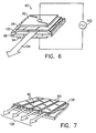
- a perspective view of a preferred TFEL image exposure device 90 is shown and it comprises a pair of metal electrodes 92, 94, interposed dielectric layers 96 and 96 and an active layer 100.
- Active layer 100 is preferably a doped zinc sulfide layer which exhibits an electroluminescent action when a proper signal is applied across metal electrodes 92, 94 from a signal source 102. Upon such excitation, active layer 100 emits light from the TFEL device's exposed edge in the direction of arrow 104.
- a plurality of TFEL devices 90 are mounted on a substrate 106 to enable a plurality of light beams 108 to be simultaneously produced in response to pixel image data (the circuitry for exciting TFEL devices 90 is not shown). Further details regarding the characteristics of TFEL exposure devices 90 can be found in: "Thin Film Electroluminescent Edge Emitter: The Imaging Station of the Future", Leksell, 5th Annual Photoreceptor and Copier Components Conference, Imaging Materials Seminar Series, Santa Barbara, 1989.
- TFEL exposure devices 90 can be rigidly mounted and do not exhibit the nonlinearities of scanned laser devices, their use in single pass color printer 10'' enables maintenance of excellent registration between subsequently toned color plane images.
- TFEL exposure devices 82, 84, and 86 In a single pass color printer such as shown in Fig. 5, TFEL exposure devices 82, 84, and 86 must expose photoreceptor web 12 through intervening toner deposits already on the web.
- the intervening deposits reduce the amount of exposure light which penetrates to the charge generation layer of photoreceptor web 12 and thereby slows the overall exposure process -- with an attendant affect on speed of operation of the printer.
- paper dust accumulates on the outer surface of photoreceptor web 12 and can occlude light from impinging on the photoreceptor.
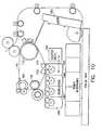
- FIG. 8 Such a configuration is shown in Fig. 8 wherein each of TFEL exposure devices 80', 82', 84', and 86' have been shifted from the position shown in Fig. 5 into the interior area within photoreceptor web 12.
- a positive charging photoreceptor 12 is required as shown schematically in Fig. 3. Since image exposure of photoreceptor web 12 is from its upper side, support 110 is made transparent to the wavelength of light emitted by TFEL image exposure devices 80', 82', 84', and 86'.
- Support 110 is supported on a transparent ground plane 112 which is in turn stacked on a charge transport layer 114, a charge generation layer 116, and a release/overcoat layer 118. Toner particles 120 are present on the lowermost surface of release/overcoat layer 118.
- photoreceptor web 12 when taking the structure shown in Fig. 3, is initially subjected to an erase module 22 which, because release/overcoat layer 118 is at least partially light transparent at the emitted wavelength enables establishment within charge generation layer 116 of electron-hole pairs in the manner known in the art.
- a corona charge module 24 acts to emplace a uniform charge on the surface of release/overcoat layer 118.
- a TFEL image exposure device e.g. 80'
- electron-hole pairs are selectively altered within charge generation layer 116 in accordance with the light pattern impressed thereupon.
- photoreceptor belt 12 Due to the positive charge polarity on the surface of release/overcoat layer 118, positive polarity charge states migrate to ground plane 112 while negative polarity charge states migrate to the interface between charge generation layer 116 and release/overcoat layer 118. Thereafter, photoreceptor belt 12 is moved into contact with a developer module and development occurs in the manner aforedescribed.
- TFEL exposure devices 82', 84' and 86' need to expose a charge generation layer through a toner layer (since the toner layer lies on the lowermost surface of release/overcoat layer 118 and the light exposure comes through transparent support 110). Furthermore, the interior surface of photoreceptor web 12 is maintained in a cleaner state as it is more sheltered with respect to paper dust.
- FIG. 9 an embodiment not part of the invention is illustrated which employs a negatively charged, dry powder, single component, dielectric toner.
- Each of developer modules 130, 132, 134 and 136 is structurally identical and includes a developer roller 138, a toner charging roller 140 and metering blade 144.
- Each developer module 130, 132, etc. is identical in structure to that shown in U.S. Patent 5,314,774 .
- each developer module applies the dry powder toner to photoreceptor web 146 in accordance with pixel charge states resident thereon.
- photoreceptor web 146 is constructed to have a transparent backing layer and ground plane so as to enable backside exposure.
- the photo conductive layer may be one of a variety of well known negatively charging photo conductors.
- TFEL image exposure devices 148, 150, 152 and 154 Oriented above the upper side of photoreceptor web 146 are a plurality of TFEL image exposure devices 148, 150, 152 and 154 which are, in structure and operation, identical to those shown in Fig. 8 and Figs. 6 and 7.
- a photoreceptor charging roller 156 and an erase head 158 Immediately upstream from each developer module is a photoreceptor charging roller 156 and an erase head 158. Further details of remaining portions of the system are discussed in US Patent 5,314,774 .
- photoreceptor belt 146 moves past each developer station, its surface is first erased and uniformly charged, followed by exposure in accordance with supplied pixel information from an associated TFEL image exposure device. The exposed image is then developed in the known manner, using the dry toner powder. Each subsequent developer module applies a different color toner in accordance with pixel charge states from a corresponding color plane. In such manner, a single pass dry powder EP printer is achieved wherein "backside" exposure is enabled.
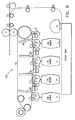
- a four pass EP printer is employed which achieves compactness of design through use of a shuttle mechanism to move developer modules into contact with a photoreceptor web. More specifically, photoreceptor web 170 is threaded over a drive roller 172 and around follower rollers 174, 176, 178, and 180.
- a single laser scanner 182 operates to form latent image charge states on photoreceptor belt 170 in accordance with color plane pixel data for each pass of belt 170.
- the mechanism further includes a plurality of developer modules 184, 186, 188, and 190, each of which is dedicated to toning a single color liquid toner (in the manner aforedescribed).
- a shuttle mechanism 192 causes an appropriate developer module to move into contact with photoreceptor web 170 at follower rollers 176, 174.
- toner module 190 is moved into contact with photoreceptor web 170.
- shuttle mechanism 192 moves developer module 188 into contact with photoreceptor web 170, etc., etc.
- a four pass color EP printer is constructed which is compact in structure and is therefore able to employ a shorter photoreceptor web 170.
Description
- This invention relates to color electrophotographic printers and, more particularly, to single pass color EP printers exhibiting improved performance characteristics.
- The prior art includes many teachings of full color electrophotographic (EP) printer configurations. Many color EP printers employ a four-pass configuration wherein four developer modules are arrayed along a photoreceptor surface. The developer modules are allocated to the deposition of cyan, yellow, magenta, and black toners onto the moving photoreceptor surface. A charging station uniformly sensitizes the photoreceptor surface. An exposure station selectively discharges the photoreceptor surface in accordance with respective color plane image data. The photoreceptor surface is then passed over the developer modules, with one developer module being brought into engagement with the photoreceptor surface to allow development of one color of the exposed image. The developed photoreceptor image then experiences a full rotation, is again exposed in accord with next color plane data and the re-exposed image is again developed, using the next color. The procedure continues until four passes have occurred and the entire full color image is present on the photoreceptor. An image transfer action then occurs whereby the color-toned image is transferred to a sheet which then issues from the printer.
U.S. Patent 5,314,774 to Camis discloses such a system and employs a plurality of dry powder, color toner developer modules to enable the operation of a four-pass coior printer. The Camis apparatus employs a non-magnetic toner which enables the use of dot-on-dot image development. -
U.S. Patent 5,300,990 to Thompson illustrates a liquid EP printer developer module and further describes (see Fig. 3) that such developer modules can be positioned side-by-side beneath a web-photoreceptor. The Thompson patent does not disclose whether the liquid EP system is single pass or four pass. Once the image in the Thompson system is fully developed on the photoreceptor surface, it is transferred to a sheet of paper or to an intermediate transfer medium. -
U.S. Patent 5,016,062 to Rapkin discloses a multicolor EP printer which includes four secondary imaging drums that are positioned along the path of an endless web. In accordance with the multi-color image to be produced, each drum is appropriately exposed in accordance with data from a single color plane and a paper sheet is passed in contact therewith via the endless web to enable toner transfer. After the sheet has contacted all of the secondary imaging drums, it contains a full color image. A similar system is shown inU.S. Patent 4,905,047 to Ariyama , however, the Ariyama system employs a liquid toner to achieve the imaging of the respective secondary drums.U.S. Patent 4,788,574 to Matsumoto et al. also discloses a four-drum/conveyor belt developer system for an in-line color printer. - To increase the speed of EP apparatus, the prior art has suggested single-pass color-printers.
European Patent 0 599 296 to Fukuchi et al. illustrates a single pass color copier which includes a four plane memory for storing yellow, magenta, cyan and black pixel data. In one embodiment, Fukuchi et al. use a web photoreceptor having a plurality of liquid toner developer modules arrayed along one surface. Between each developer module, a laser beam images the web photoreceptor in accordance with a particular color plane's pixel data. Immediately after each imaging action, a development occurs in accordance with the charge states on the web photoreceptor. Next, the web photoreceptor is again charged and developed in accordance with a next color plane's image data. The procedure continues until all four image planes have been exposed and developed, at which point the image is transferred to a paper sheet. Fukuchi et al. employ powder toners to achieve their individual color toning actions. -
U.S. Patent 4,599,285 to Haneda et al. discloses an EP apparatus wherein plural developers are positioned along a photoreceptor web, with each developer module employing a two-component powder toner. Electrostatic recording heads are positioned between the individual developer modules to allow a writing of pixel charge states on the photoreceptor web in accordance with particular color plane data. - While it is known that the speed of a single pass color EP printer can be made four times faster than a four-pass print architecture, single-pass EP color printers present a number of problems. It is difficult to assure proper registration of subsequent image color planes if the photoreceptor web is subject to speed variations as a result of engagement and disengagement of developer modules. Web speed variations cause a "banding" in the image and are to be avoided. In EP color printers that employ liquid toners, a line of fluid is created by surface tension of the toner carrier when a wetted roller or blade is removed from the surface of the photoreceptor. Means are generally provided to remove the "drip" line so as to prevent it from contaminating the system. Further, complex apparatus is required to enable engagement and disengagement of developer modules and transfer rollers from the photoreceptor web. The speed of the EP printer is further dependent upon the time it takes to disengage a developer module and engage a next developer, etc.
-
US-A-5,241,356 discloses a multi-color imaging apparatus. This multi-color imaging apparatus basically uses two different development approaches, namely the so-called "CAD approach" (charged area development) and the "DAD approach" (discharged area development). In a first developer station C, the charged area development (CAD) is effected, whereas as in a second development station, the discharged area development (DAD) is carried out. In the two development stations C and D, a so-called "post CAD"erase lamp 34 is provided, which serves to reduce the charge level of the photoreceptor in the toned or developed areas. -
US-A-5,272,508 concerns an electrophotographic photosensitive member and is basically concerned with the specific structure of a drum-shaped or endless-shaped light transmissive carrier used in electrophotographic printing. -
EP-A-0 398 592 discloses the use of thin film electroluminescent edge emitters in electrophotographic printing. However, the printer does not provide four erase means inbetween respective development modules, as is taught by the present invention. -
JP-A-02 106367 - It is the object of the present invention to provide an improved electrophotographic printer.
- This object is achieved by an electrophotographic printer according to claim 1.
- According to the present invention, a single pass full color EP printer exhibiting an improved architecture and speed of operation is provided. Further, an improved full color EP printer is provided that employs liquid toner developer modules, but avoids drip lines on the photoreceptor. Moreover, an improved full color EP printer is provided wherein mechanisms to engage and disengage developer modules are avoided.
- A single pass EP color printer includes a photoreceptor web having multiple layers and including a charge transport layer and a charge generation layer. Four exposure devices (e.g. either laser-based or thin film electroluminescent edge emitting (TFEL) devices) are serially arrayed along the photoreceptor web and act to expose the photoreceptor web in accordance with cyan, magenta, yellow and black color image pixel data. A liquid toner developer module is associated with each exposure device and includes a liquid toner reservoir, a developer roll for carrying the liquid toner to a transfer point and a squeegee roll. Each developer module is fixed so as to position its developer roll at a constant prescribed distance from the photoreceptor web at the toner transfer point and to create a fluid interfacial layer between its developer roll and the photoreceptor web. In addition, each squeegee roll is maintained in constant contact with the photoreceptor web. Erasure devices and corona charging devices are positioned between the respective developer modules to enable preparation of the photoreceptor web for a subsequent exposure/development operation. A drying roll is positioned after a last developer module for fixing the imaged toner on the photoreceptor web. The exposure devices operate from either the lower side of the photoreceptor web or from the upper side; however, in the latter instance, the photoreceptor web is comprised of a transparent support and ground plane layer.
-
- Fig. 1 is a schematic showing a first embodiment of a liquid toner EP printer constructed in accordance with the invention.
- Fig. 1a is an enlarged view of the developer roll/photoreceptor web nip.
- Fig. 2 is a sectional view of an inverted dual layer photoreceptor wherein optical exposure occurs through the release/overcoat layer.
- Fig. 3 is a section of an inverted dual layer photoreceptor wherein exposure occurs through a transparent support.
- Fig. 4 is an embodiment of the invention of Fig. 1 wherein a drying roll is positioned between each developer module.
- Fig. 5 is a schematic embodiment of the invention wherein the photoreceptor is exposed by a TFEL device.
- Fig. 6 illustrates a TFEL device.
- Fig. 7 illustrates an array of TFEL devices.
- Fig. 8 is a schematic embodiment of the invention wherein TFEL devices are employed to expose the photoreceptor, but from an upper surface thereof.
- Fig. 9 is a schematic view of a single-pass dry toner EP printer which employs TFEL devices.
- Fig. 10 is a schematic view of a four pass color EP printer wherein liquid toner developer modules are mounted on a shuttle so as to enable a more compact arrangement of the EP printer.
- Fig. 1 illustrates a schematic representation of a single-pass, liquid toner, multi-color,
EP printer 10 incorporating the invention. Aphotoreceptor web 12 is positioned overdrive roller 14 andfollower rollers Photoreceptor web 12 is further engaged by four separate developer stations, each developer station being structurally identical but applying a different color liquid toner tophotoreceptor web 12. Each developer station (e.g. 20) includes an erasehead 22, acorona charge module 24, a scanninglaser write head 26, adeveloper module 28 and aliquid toner reservoir 30.Reservoir 30, in the example shown in Fig. 1, contains a cyan liquid toner including both a toner component and a dispersant component (e.g. Isopar™ or Norpar™, as available from the Exxon Corporation). Additional developer stations, 32, 34, and 36 are arrayed linearly alongphotoreceptor web 12 and provide exposure and developing functions for magenta, yellow and black toners.Developer station 20 will be hereafter described in detail, but it is to be understood that each ofdeveloper stations - While not shown, those skilled in the art will realize that
EP printer 10 includes a processor and a resident memory, which includes memory planes reserved for pixel data representing cyan, magenta, yellow and black pixel data that is to printed. For the example shown in Fig. 1, data resident in the processor's memory that is representative of cyan pixel data is fed (in signal form) tolaser 26 which is, in turn, scanned acrossphotoreceptor web 12 to create corresponding pixel charge states thereon. Prior to the scan action, an erasehead 22 is operated to dischargephotoreceptor web 12. Erasehead 22 preferably comprises a light source that spans the width ofphotoreceptor web 12 and causes an erasure of previously written pixel data. Immediately following erasehead 22 is acorona charge module 24 which causesphotoreceptor web 12 to achieve a uniform charge state across its width. - After
corona charge module 24 has chargedphotoreceptor web 12 to a uniform charge state,laser module 26 is scanned to write a cyan pixel image across the width ofphotoreceptor web 12. Thereafter, the image-containing portion ofphotoreceptor web 12 is moved throughdeveloper module 28 which, in this preferred embodiment, is in continual engagement withphotoreceptor web 12.Developer module 28 is supplied with cyan liquid toner fromliquid toner reservoir 30.Developer roll 38 receives the cyan liquid toner and entrains that toner around its outer periphery to atransfer point 39. As shown in Fig. 1a,developer roll 38 is not in physical contact withphotoreceptor web 12 but is spaced therefrom by a prescribed distance so as to create a fluid interfacial layer attransfer point 39 so as to enable migration of toner particles in the liquid toner to the appropriately discharged areas onphotoreceptor web 12. The distance betweenphotoreceptor web 12 anddeveloper roll 38 is assured by proper adjustment of acam 40. - Immediately following
developer roll 38 is asqueegee roll 42 which rotates in a direction coincident with the direction of movement ofphotoreceptor web 12.Squeegee roll 42 enables the removal of a substantial percentage of the solvent from the toner present onphotoreceptor web 12 and enables the cyan-toned image to emerge fromdeveloper module 28 in a substantially dry state. In fact, it has been found that the exiting cyan-toned image is sufficiently dry, given proper adjustment ofdeveloper module 28, to enable an immediate subsequent toning by a further liquid toner. - Excess liquid toner from the toning and squeegee actions in
toner module 28 is captured by anenclosure 44 and is returned toliquid toner reservoir 30 for reuse. Each of the developer modules indeveloper stations photoreceptor web 12. As a result, no load variations occur onphotoreceptor web 12 due to engagement and disengagement of the respective developer modules. Further, no drip line is created by disengagement of a developer module fromphotoreceptor web 12. In addition, there is no requirement for individual drying rolls to be positioned between the respective developer stations. For that reason, only asingle drying roll 46 is present at the outlet fromdeveloper station 36. - As above indicated, each of
developer stations printer 10. Thus, afterdeveloper station 20 has completed its toning of the cyan pixel data onphotoreceptor web 12, the toned image is moved todeveloper station 32 wherephotoreceptor web 12 is charged and exposed in accord with magenta pixel data and is then appropriately toned with magenta toner. Subsequently, the cyan/magenta toned image is moved todeveloper stations sheet 50.Sheet 50, as is known in the art, is fed from apaper tray 52 under control of arotatable cam 54 andfeed rollers - Referring to Fig. 2, a cross section is shown of a preferred embodiment of
photoreceptor web 12. A substrate/ground plane 60 forms a support layer and has arrayed on it acharge transport layer 62, acharge generation layer 64 and a release/overcoat layer 66.Charge generation layer 64 responds to incident laser light to generate corresponding charge pairs.Charge transport layer 62 provides a charge travel path which allows migration of certain charges states to groundplane 60 while other charge states migrate to the interface betweencharge generation layer 64 and release/overcoat layer 66. Becausecharge generation layer 64 is very close to the surface ofphotoreceptor belt 12 and is extremely thin, its speed of photo response is excellent. Further, ghosting effects are minimized due to the thinness ofcharge generation layer 64 and the higher penetration of light during both exposure and erasing actions. Exemplary thicknesses for the layers are as follows: charge generation layer 64: 0.1 µm, charge transport layer 62: 15 µm. A preferred material for the charge generation layer is a metal-free phthalocyanine. The charge transport layer is comprised of charge transport molecules dispersed in an inert binder. Further details regarding a photoreceptor such as shown in Fig. 2 can be found in Organic Photoconductors For Imaging System, Borsenberger et al., Published by M. Dekker Inc., New York (1993). - As above indicated,
developer modules 28, if properly adjusted, assure that toned images exiting therefrom are sufficiently dry to receive additional layers of toner. To lessen the adjustment requirements, the modified structure shown in Fig. 4 is employed. Each of developer stations 20', 32', 34', and 36' is structurally identical to that shown in Fig. 1, except that each developer station now includes a dryingroll 70 and amating roll 72. The inclusion of a dryingroll 70 with each developer station, increases the overall length and complexity of the printer structure but provides further assurance that a dry toned surface will enter a subsequent developer station. Mating rolls 72 assure thatbelt 12 is pressed against dryingroll 70 with sufficient pressure so that the toner present onphotoreceptor web 12 is fixed by a combination of the pressure and heat applied via dryingroll 70. - The EP printers shown in Fig. 1 and Fig. 4 employ
scanning laser modules 26 to achieve desired pixel charge states onphotoreceptor web 12. Since a single pass color printer requires a subsequent color plane image to be precisely registered with a previously toned color image, it is critical that the placement oflaser modules 26 be precisely controlled. Further, laser scanners exhibit errors of scale, bow, linearity and intensity that need to be matched and adjusted. Additionally, laser scanners are subject to vibration and other environmental effects which may cause registration problems. The use of a TFEL device obviates many of the problems associated with the laser scanner. - In Fig. 5, a single pass multicolor printer 10' includes
TFEL exposure devices photoreceptor web 12 in accordance with pixel data as aforedescribed. In Fig. 5, each developer station 20'', 32", 34'', 36'' is identical to that shown in Fig. 1, except that theresident laser module 26 has been replaced by a TFEL image exposure device. In Fig. 6, a perspective view of a preferred TFELimage exposure device 90 is shown and it comprises a pair ofmetal electrodes dielectric layers active layer 100.Active layer 100 is preferably a doped zinc sulfide layer which exhibits an electroluminescent action when a proper signal is applied acrossmetal electrodes signal source 102. Upon such excitation,active layer 100 emits light from the TFEL device's exposed edge in the direction ofarrow 104. - In Fig. 7, a plurality of
TFEL devices 90 are mounted on asubstrate 106 to enable a plurality oflight beams 108 to be simultaneously produced in response to pixel image data (the circuitry forexciting TFEL devices 90 is not shown). Further details regarding the characteristics ofTFEL exposure devices 90 can be found in: "Thin Film Electroluminescent Edge Emitter: The Imaging Station of the Future", Leksell, 5th Annual Photoreceptor and Copier Components Conference, Imaging Materials Seminar Series, Santa Barbara, 1989. - Because
TFEL exposure devices 90 can be rigidly mounted and do not exhibit the nonlinearities of scanned laser devices, their use in single pass color printer 10'' enables maintenance of excellent registration between subsequently toned color plane images. - In a single pass color printer such as shown in Fig. 5,
TFEL exposure devices photoreceptor web 12 through intervening toner deposits already on the web. The intervening deposits reduce the amount of exposure light which penetrates to the charge generation layer ofphotoreceptor web 12 and thereby slows the overall exposure process -- with an attendant affect on speed of operation of the printer. Further, because of the substantial amount of paper which moves withinprinter 10, paper dust accumulates on the outer surface ofphotoreceptor web 12 and can occlude light from impinging on the photoreceptor. These problems can be overcome by employing an altered photoreceptor web configuration and placing each of the TFEL exposure devices above the upper surface ofphotoreceptor web 12. - Such a configuration is shown in Fig. 8 wherein each of TFEL exposure devices 80', 82', 84', and 86' have been shifted from the position shown in Fig. 5 into the interior area within
photoreceptor web 12. In the system shown in Fig. 8, since discharge area development is preferred and the preferred liquid toner is positively charged, apositive charging photoreceptor 12 is required as shown schematically in Fig. 3. Since image exposure ofphotoreceptor web 12 is from its upper side, support 110 is made transparent to the wavelength of light emitted by TFEL image exposure devices 80', 82', 84', and 86'. Support 110 is supported on atransparent ground plane 112 which is in turn stacked on acharge transport layer 114, acharge generation layer 116, and a release/overcoat layer 118.Toner particles 120 are present on the lowermost surface of release/overcoat layer 118. - In operation,
photoreceptor web 12, when taking the structure shown in Fig. 3, is initially subjected to an erasemodule 22 which, because release/overcoat layer 118 is at least partially light transparent at the emitted wavelength enables establishment withincharge generation layer 116 of electron-hole pairs in the manner known in the art. Thereafter, acorona charge module 24 acts to emplace a uniform charge on the surface of release/overcoat layer 118. Then, a TFEL image exposure device (e.g. 80') is controlled to selectively exposephotoreceptor web 12 throughtransparent support 10 andground plane 112. As a result, electron-hole pairs are selectively altered withincharge generation layer 116 in accordance with the light pattern impressed thereupon. Due to the positive charge polarity on the surface of release/overcoat layer 118, positive polarity charge states migrate to groundplane 112 while negative polarity charge states migrate to the interface betweencharge generation layer 116 and release/overcoat layer 118. Thereafter,photoreceptor belt 12 is moved into contact with a developer module and development occurs in the manner aforedescribed. - By placing the TFEL image exposure devices within the interior of
photoreceptor web 12, no longer do TFEL exposure devices 82', 84' and 86' need to expose a charge generation layer through a toner layer (since the toner layer lies on the lowermost surface of release/overcoat layer 118 and the light exposure comes through transparent support 110). Furthermore, the interior surface ofphotoreceptor web 12 is maintained in a cleaner state as it is more sheltered with respect to paper dust. - In Fig. 9, an embodiment not part of the invention is illustrated which employs a negatively charged, dry powder, single component, dielectric toner. Each of
developer modules developer roller 138, a toner charging roller 140 andmetering blade 144. Eachdeveloper module 130, 132, etc. is identical in structure to that shown inU.S. Patent 5,314,774 . - In the known manner, each developer module applies the dry powder toner to
photoreceptor web 146 in accordance with pixel charge states resident thereon. In this case,photoreceptor web 146 is constructed to have a transparent backing layer and ground plane so as to enable backside exposure. The photo conductive layer may be one of a variety of well known negatively charging photo conductors. Oriented above the upper side ofphotoreceptor web 146 are a plurality of TFELimage exposure devices photoreceptor charging roller 156 and an erase head 158. Further details of remaining portions of the system are discussed inUS Patent 5,314,774 . - As
photoreceptor belt 146 moves past each developer station, its surface is first erased and uniformly charged, followed by exposure in accordance with supplied pixel information from an associated TFEL image exposure device. The exposed image is then developed in the known manner, using the dry toner powder. Each subsequent developer module applies a different color toner in accordance with pixel charge states from a corresponding color plane. In such manner, a single pass dry powder EP printer is achieved wherein "backside" exposure is enabled. - In Fig. 10, a four pass EP printer is employed which achieves compactness of design through use of a shuttle mechanism to move developer modules into contact with a photoreceptor web. More specifically,
photoreceptor web 170 is threaded over adrive roller 172 and aroundfollower rollers single laser scanner 182 operates to form latent image charge states onphotoreceptor belt 170 in accordance with color plane pixel data for each pass ofbelt 170. The mechanism further includes a plurality ofdeveloper modules - Assuming that
developer modules shuttle mechanism 192 causes an appropriate developer module to move into contact withphotoreceptor web 170 atfollower rollers laser scanner 182images photoreceptor web 170 in accordance with pixel data from a cyan memory plane,toner module 190 is moved into contact withphotoreceptor web 170. Upon a next rotation ofphotoreceptor web 170past laser scanner 182, charge states in accordance with pixel data from a yellow memory plane are applied andshuttle mechanism 192 movesdeveloper module 188 into contact withphotoreceptor web 170, etc., etc. In such manner, a four pass color EP printer is constructed which is compact in structure and is therefore able to employ ashorter photoreceptor web 170. - It should be understood that the foregoing description is only illustrative of the invention. Various alternatives and modifications can be devised by those skilled in the art without departing from the invention as defined in the appended claims. For instance, while the liquid toner aspects invention have been described in the context of a positively charged photoreceptor, a system employing a negatively charged photoreceptor also falls within the scope of the invention. Accordingly, the present invention is intended to embrace all such alternatives, modifications and variances which fall within the scope of the appended claims.
Claims (8)
- An electrophotographic color printer (10) comprising:a photoreceptor (12) having a toner-receiving surface;means (14, 16, 18) for moving said photoreceptor (12) in a first direction of movement;plural exposure means (26, 80, 82, 84, 86) arrayed along said toner-receiving surface (66, 118) of said photoreceptor (12) for discharging said photoreceptor in accordance with different color image pixel values;a developer module (28) associated with each exposure means, each said developer module including a liquid toner reservoir (30), a developer roll (38) for carrying liquid toner to a transfer point (39), a squeegee roll (42) for removing excess dispersant from said liquid toner after said liquid toner has been applied to said photoreceptor (12), said developer module (28) maintaining said developer roll (38) at a constant distance from said photoreceptor (12) at said transfer point (39) to create a fluid interfacial layer thereat between said developer roll (38) and said photoreceptor (12), said developer module (28) further maintaining said squeegee roll (42) in constant engagement with said photoreceptor (12);an erase means (22) positioned upstream from each said exposure means (26, 80, 82, 84, 86) in regards to said first direction of movement of said photoreceptor (12);charge means (24) positioned between each said erase means (22) and a downstream exposure means (26, 80, 82, 86);a drying roll (46) positioned after the last developer module (26) for fixing a toner image on said photoreceptor (12); andmeans for transferring (48) said toner image to a sheet (50).
- The electrophotographic color printer (10) as recited in claim 1, wherein said photoreceptor (12) is a web, said toner-receiving surface (66, 118) being a release layer, said web further comprising a plurality of layers positioned on said release layer, said layers including: a charge generation layer (64, 116), a charge transport layer (62, 114), and a substrate/ground plane layer (60, 110, 112).
- The electrophotographic color printer (10) as recited in claim 2 whereon said layers are positioned on said release layer (66, 118) in the order recited.
- The electrophotographic color printer (10) as recited in claim 2 wherein each of said plural exposure means (26) includes a scanning laser beam generator.
- The electrophotographic color printer (10) as recited in claim 2 wherein each of said plural exposure means (80, 82, 84, 86) comprises a linear array of edge-emitting optical transmitters (90) juxtaposed to said toner-receiving surface (66) of said photoreceptor (12).
- The electrophotographic color printer (10) as recited in claim 1 wherein only a single drying roll (46) is positioned in contact with said photoreceptor (12).
- The electrophotographic color printer (10) as recited in claim 1, further comprising:plural additional drying rolls (70), each drying roll (70) positioned immediately downstream in said first direction of movement from an associated developer module (28).
- The electrophotographic color printer (10) as recited in claim 1 wherein said photoreceptor (12) is a web and wherein said toner-receiving surface comprises a release/overcoat layer (112) and further includes a stack of layers positioned thereon in a following order: a charge generation layer (116), a charge transport layer (114), a transparent ground plane layer (112), and a transparent support (110) comprising an upper surface of said photoreceptor (12), and wherein each said exposure means is an array of edge emitting optical transmitters (90) juxtaposed to said transparent support (110) and over said upper surface.
Priority Applications (1)
| Application Number | Priority Date | Filing Date | Title |
|---|---|---|---|
| EP00123004A EP1070992B1 (en) | 1995-05-30 | 1996-04-30 | In-line color electrophotographic printer |
Applications Claiming Priority (2)
| Application Number | Priority Date | Filing Date | Title |
|---|---|---|---|
| US08/455,011 US5557377A (en) | 1995-05-30 | 1995-05-30 | Single pass, in-line color electrophotographic printer with interspersed erase device |
| US455011 | 1995-05-30 |
Related Child Applications (1)
| Application Number | Title | Priority Date | Filing Date |
|---|---|---|---|
| EP00123004A Division EP1070992B1 (en) | 1995-05-30 | 1996-04-30 | In-line color electrophotographic printer |
Publications (3)
| Publication Number | Publication Date |
|---|---|
| EP0745909A2 EP0745909A2 (en) | 1996-12-04 |
| EP0745909A3 EP0745909A3 (en) | 1998-12-09 |
| EP0745909B1 true EP0745909B1 (en) | 2008-01-02 |
Family
ID=23806999
Family Applications (2)
| Application Number | Title | Priority Date | Filing Date |
|---|---|---|---|
| EP00123004A Expired - Lifetime EP1070992B1 (en) | 1995-05-30 | 1996-04-30 | In-line color electrophotographic printer |
| EP96106852A Expired - Lifetime EP0745909B1 (en) | 1995-05-30 | 1996-04-30 | In-line color electrophotographic printer |
Family Applications Before (1)
| Application Number | Title | Priority Date | Filing Date |
|---|---|---|---|
| EP00123004A Expired - Lifetime EP1070992B1 (en) | 1995-05-30 | 1996-04-30 | In-line color electrophotographic printer |
Country Status (4)
| Country | Link |
|---|---|
| US (1) | US5557377A (en) |
| EP (2) | EP1070992B1 (en) |
| JP (1) | JPH096081A (en) |
| DE (2) | DE69637475T2 (en) |
Families Citing this family (20)
| Publication number | Priority date | Publication date | Assignee | Title |
|---|---|---|---|---|
| US5752137A (en) * | 1995-06-09 | 1998-05-12 | Konica Corporation | Multi-color image forming apparatus having a plurality of detachable units |
| US5666607A (en) * | 1996-01-11 | 1997-09-09 | Hewlett-Packard Company | Wet contact charging for electrophotography |
| JPH09218556A (en) * | 1996-02-13 | 1997-08-19 | Konica Corp | Color image forming device |
| JPH1031342A (en) * | 1996-05-15 | 1998-02-03 | Sharp Corp | Image forming device |
| US6191801B1 (en) * | 1996-07-09 | 2001-02-20 | Aetas Peripheral Corporation | Color electrophotographic apparauts having image registration |
| JP2933040B2 (en) * | 1996-12-16 | 1999-08-09 | 日本電気株式会社 | Image forming device |
| US5812913A (en) * | 1997-01-06 | 1998-09-22 | Minnesota Mining And Manufacturing Company | Method and apparatus to dry media during electrostatic printing |
| US6249305B1 (en) * | 1997-05-16 | 2001-06-19 | Konica Corporation | Color image forming apparatus |
| KR200147792Y1 (en) * | 1997-06-30 | 1999-06-15 | 윤종용 | Liquid electrophotographic printer |
| US6141026A (en) * | 1997-10-31 | 2000-10-31 | Xerox Corporation | Liquid ink development control |
| KR100265736B1 (en) * | 1997-12-08 | 2000-09-15 | 윤종용 | Electrophotographic printer |
| KR100331306B1 (en) * | 1998-05-07 | 2002-05-09 | 윤종용 | Wet printer |
| US6198890B1 (en) | 1999-10-06 | 2001-03-06 | Aetas Technology Corporation | Electrophotographic color printing arrangement with inclined photoreceptor path |
| KR100370204B1 (en) | 1999-10-27 | 2003-01-29 | 삼성전자 주식회사 | A photoreceptor belt for liquid electrophotographic printer |
| US6311033B1 (en) * | 2000-02-11 | 2001-10-30 | Aetas Technology Corporation | Electrophotographic exposure and development arrangement |
| US6370354B1 (en) | 2000-08-08 | 2002-04-09 | Lexmark International, Inc. | Method and apparatus for controlling media-to-image registration of a single-pass intermediate transfer member-based printing apparatus |
| US6262753B1 (en) * | 2000-08-16 | 2001-07-17 | Lexmark International, Inc. | Electrophotographic imaging apparatus with reduced packaging size |
| JP3602784B2 (en) | 2000-09-18 | 2004-12-15 | 株式会社東芝 | Electrophotographic apparatus and manufacturing method thereof |
| JP3692024B2 (en) | 2000-10-13 | 2005-09-07 | 株式会社東芝 | Image forming apparatus and image forming method |
| US7920810B2 (en) | 2007-08-15 | 2011-04-05 | Hewlett-Packard Development Company, L.P. | Electrophotography device with electric field applicator |
Family Cites Families (18)
| Publication number | Priority date | Publication date | Assignee | Title |
|---|---|---|---|---|
| JPS6059592B2 (en) * | 1981-09-11 | 1985-12-25 | 日本電信電話株式会社 | Recording method |
| DE3483877D1 (en) * | 1983-10-03 | 1991-02-07 | Konishiroku Photo Ind | MI-MULTIPLE IMAGE REPRODUCTION PROCESS. |
| JPS6177866A (en) * | 1984-09-26 | 1986-04-21 | Ishihara Sangyo Kaisha Ltd | Color electrophotographic method |
| JPS6255674A (en) * | 1985-09-03 | 1987-03-11 | Canon Inc | Color image forming device for transferring successively toner image from plural image carrying bodies |
| JPS62238585A (en) * | 1986-04-09 | 1987-10-19 | Asahi Optical Co Ltd | Multi-color image forming method for electrophotographic method |
| US4761669A (en) * | 1987-05-21 | 1988-08-02 | Xerox Corporation | Highlight color printing |
| JPH01112264A (en) * | 1987-10-26 | 1989-04-28 | Seiko Epson Corp | Color printing method |
| US4905047A (en) * | 1988-02-12 | 1990-02-27 | Ricoh Company, Ltd. | Wet type image forming apparatus |
| US5043715A (en) * | 1988-12-07 | 1991-08-27 | Westinghouse Electric Corp. | Thin film electroluminescent edge emitter structure with optical lens and multi-color light emission systems |
| JPH02106367A (en) * | 1988-10-15 | 1990-04-18 | Nippon Telegr & Teleph Corp <Ntt> | Color printer |
| US5272508A (en) * | 1989-10-19 | 1993-12-21 | Canon Kabushiki Kaisha | Electrophotographic photosensitive member and apparatus incorporating the same |
| US5016062A (en) * | 1990-01-02 | 1991-05-14 | Eastman Kodak Company | Multicolor image forming apparatus having improved registration |
| JPH05273800A (en) * | 1992-03-25 | 1993-10-22 | Toray Ind Inc | Electrophotographic printer |
| JPH05307307A (en) * | 1992-04-28 | 1993-11-19 | Ricoh Co Ltd | Color image forming device |
| US5314774A (en) * | 1992-05-22 | 1994-05-24 | Hewlett-Packard Company | Method and apparatus for developing color images using dry toners and an intermediate transfer member |
| US5300990A (en) * | 1992-06-26 | 1994-04-05 | Hewlett-Packard Company | Liquid electrophotographic printer developer |
| US5241356A (en) * | 1992-07-29 | 1993-08-31 | Xerox Corporation | Method and apparatus for minimizing the voltage difference between a developed electrostatic image area and a latent electrostaic non-developed image |
| JPH06164876A (en) * | 1992-11-26 | 1994-06-10 | Konica Corp | Color picture forming device |
-
1995
- 1995-05-30 US US08/455,011 patent/US5557377A/en not_active Expired - Lifetime
-
1996
- 1996-04-30 EP EP00123004A patent/EP1070992B1/en not_active Expired - Lifetime
- 1996-04-30 EP EP96106852A patent/EP0745909B1/en not_active Expired - Lifetime
- 1996-04-30 DE DE69637475T patent/DE69637475T2/en not_active Expired - Lifetime
- 1996-04-30 DE DE69637386T patent/DE69637386T2/en not_active Expired - Lifetime
- 1996-05-30 JP JP8136404A patent/JPH096081A/en active Pending
Also Published As
| Publication number | Publication date |
|---|---|
| JPH096081A (en) | 1997-01-10 |
| DE69637475D1 (en) | 2008-05-08 |
| US5557377A (en) | 1996-09-17 |
| EP0745909A2 (en) | 1996-12-04 |
| DE69637386D1 (en) | 2008-02-14 |
| EP1070992A3 (en) | 2002-08-21 |
| EP0745909A3 (en) | 1998-12-09 |
| DE69637475T2 (en) | 2009-04-16 |
| EP1070992A2 (en) | 2001-01-24 |
| DE69637386T2 (en) | 2009-01-29 |
| EP1070992B1 (en) | 2008-03-26 |
Similar Documents
| Publication | Publication Date | Title |
|---|---|---|
| EP0745909B1 (en) | In-line color electrophotographic printer | |
| KR100310589B1 (en) | Electrostatic Photo Diary One-pass multi-station printer for two-sided printing | |
| EP0606141B1 (en) | Dual electrophotographic color printing with ROS and dual layer photoreceptor | |
| EP0602339B1 (en) | Image development and transfer method and apparatus for an electrophotographic color printer | |
| EP0893909A2 (en) | Image forming device | |
| JP3379803B2 (en) | Color xerographic printing apparatus using two-wavelength single optical system ROS and two-layer photoreceptor | |
| JP4240198B2 (en) | Exposure head and image forming apparatus using the same | |
| US4937636A (en) | Single pass, two-color electrophotographic reproduction machine | |
| US6011575A (en) | Image forming apparatus with line-shaped image exposure means | |
| EP0549575B1 (en) | Liquid developer systems for imaging on transparent and opaque substrates | |
| JP2004082330A (en) | Exposure head and image formation apparatus using it | |
| US4969012A (en) | Image recording apparatus with an intermediate photosensitive member | |
| US5083144A (en) | Electrophotographic with scanning process module | |
| US4804980A (en) | Laser addressed ionography | |
| US20040005170A1 (en) | Image forming device | |
| US20050117014A1 (en) | Led print head printing | |
| US4956649A (en) | Image recording apparatus forming photomasking pattern on photosensitive medium | |
| JP3036144B2 (en) | Electrophotographic equipment | |
| JP2912258B2 (en) | Back exposure recording image forming device | |
| JPH09114322A (en) | Electrophotographic device | |
| US5493387A (en) | Thick overcoated PR and color on color | |
| JP3272057B2 (en) | Electrophotographic equipment | |
| US5548391A (en) | Process color using light lens scanning techniques | |
| JPH0545997A (en) | Image forming device | |
| JP2011008226A (en) | Image forming device |
Legal Events
| Date | Code | Title | Description |
|---|---|---|---|
| PUAI | Public reference made under article 153(3) epc to a published international application that has entered the european phase |
Free format text: ORIGINAL CODE: 0009012 |
|
| AK | Designated contracting states |
Kind code of ref document: A2 Designated state(s): DE FR GB |
|
| PUAL | Search report despatched |
Free format text: ORIGINAL CODE: 0009013 |
|
| AK | Designated contracting states |
Kind code of ref document: A3 Designated state(s): DE FR GB |
|
| 17P | Request for examination filed |
Effective date: 19990129 |
|
| 17Q | First examination report despatched |
Effective date: 20000614 |
|
| RAP1 | Party data changed (applicant data changed or rights of an application transferred) |
Owner name: HEWLETT-PACKARD COMPANY, A DELAWARE CORPORATION |
|
| GRAP | Despatch of communication of intention to grant a patent |
Free format text: ORIGINAL CODE: EPIDOSNIGR1 |
|
| GRAS | Grant fee paid |
Free format text: ORIGINAL CODE: EPIDOSNIGR3 |
|
| GRAA | (expected) grant |
Free format text: ORIGINAL CODE: 0009210 |
|
| AK | Designated contracting states |
Kind code of ref document: B1 Designated state(s): DE FR GB |
|
| REG | Reference to a national code |
Ref country code: GB Ref legal event code: FG4D |
|
| REF | Corresponds to: |
Ref document number: 69637386 Country of ref document: DE Date of ref document: 20080214 Kind code of ref document: P |
|
| ET | Fr: translation filed | ||
| PLBE | No opposition filed within time limit |
Free format text: ORIGINAL CODE: 0009261 |
|
| STAA | Information on the status of an ep patent application or granted ep patent |
Free format text: STATUS: NO OPPOSITION FILED WITHIN TIME LIMIT |
|
| 26N | No opposition filed |
Effective date: 20081003 |
|
| PGFP | Annual fee paid to national office [announced via postgrant information from national office to epo] |
Ref country code: DE Payment date: 20110427 Year of fee payment: 16 |
|
| PGFP | Annual fee paid to national office [announced via postgrant information from national office to epo] |
Ref country code: GB Payment date: 20110426 Year of fee payment: 16 |
|
| REG | Reference to a national code |
Ref country code: GB Ref legal event code: 732E Free format text: REGISTERED BETWEEN 20120329 AND 20120404 |
|
| PGFP | Annual fee paid to national office [announced via postgrant information from national office to epo] |
Ref country code: FR Payment date: 20120503 Year of fee payment: 17 |
|
| GBPC | Gb: european patent ceased through non-payment of renewal fee |
Effective date: 20120430 |
|
| PG25 | Lapsed in a contracting state [announced via postgrant information from national office to epo] |
Ref country code: GB Free format text: LAPSE BECAUSE OF NON-PAYMENT OF DUE FEES Effective date: 20120430 |
|
| REG | Reference to a national code |
Ref country code: DE Ref legal event code: R119 Ref document number: 69637386 Country of ref document: DE Effective date: 20121101 |
|
| REG | Reference to a national code |
Ref country code: FR Ref legal event code: ST Effective date: 20131231 |
|
| PG25 | Lapsed in a contracting state [announced via postgrant information from national office to epo] |
Ref country code: FR Free format text: LAPSE BECAUSE OF NON-PAYMENT OF DUE FEES Effective date: 20130430 |
|
| PG25 | Lapsed in a contracting state [announced via postgrant information from national office to epo] |
Ref country code: DE Free format text: LAPSE BECAUSE OF NON-PAYMENT OF DUE FEES Effective date: 20121101 |