EP0744764A2 - Method and apparatus for manufacture of semiconductor devices - Google Patents
Method and apparatus for manufacture of semiconductor devices Download PDFInfo
- Publication number
- EP0744764A2 EP0744764A2 EP96303562A EP96303562A EP0744764A2 EP 0744764 A2 EP0744764 A2 EP 0744764A2 EP 96303562 A EP96303562 A EP 96303562A EP 96303562 A EP96303562 A EP 96303562A EP 0744764 A2 EP0744764 A2 EP 0744764A2
- Authority
- EP
- European Patent Office
- Prior art keywords
- cassette
- reticle
- original
- semiconductor device
- storage means
- Prior art date
- Legal status (The legal status is an assumption and is not a legal conclusion. Google has not performed a legal analysis and makes no representation as to the accuracy of the status listed.)
- Granted
Links
Images
Classifications
-
- H—ELECTRICITY
- H01—ELECTRIC ELEMENTS
- H01L—SEMICONDUCTOR DEVICES NOT COVERED BY CLASS H10
- H01L21/00—Processes or apparatus adapted for the manufacture or treatment of semiconductor or solid state devices or of parts thereof
- H01L21/02—Manufacture or treatment of semiconductor devices or of parts thereof
- H01L21/027—Making masks on semiconductor bodies for further photolithographic processing not provided for in group H01L21/18 or H01L21/34
-
- G—PHYSICS
- G03—PHOTOGRAPHY; CINEMATOGRAPHY; ANALOGOUS TECHNIQUES USING WAVES OTHER THAN OPTICAL WAVES; ELECTROGRAPHY; HOLOGRAPHY
- G03F—PHOTOMECHANICAL PRODUCTION OF TEXTURED OR PATTERNED SURFACES, e.g. FOR PRINTING, FOR PROCESSING OF SEMICONDUCTOR DEVICES; MATERIALS THEREFOR; ORIGINALS THEREFOR; APPARATUS SPECIALLY ADAPTED THEREFOR
- G03F7/00—Photomechanical, e.g. photolithographic, production of textured or patterned surfaces, e.g. printing surfaces; Materials therefor, e.g. comprising photoresists; Apparatus specially adapted therefor
- G03F7/70—Microphotolithographic exposure; Apparatus therefor
- G03F7/70691—Handling of masks or workpieces
- G03F7/70733—Handling masks and workpieces, e.g. exchange of workpiece or mask, transport of workpiece or mask
- G03F7/70741—Handling masks outside exposure position, e.g. reticle libraries
-
- H—ELECTRICITY
- H01—ELECTRIC ELEMENTS
- H01L—SEMICONDUCTOR DEVICES NOT COVERED BY CLASS H10
- H01L21/00—Processes or apparatus adapted for the manufacture or treatment of semiconductor or solid state devices or of parts thereof
- H01L21/67—Apparatus specially adapted for handling semiconductor or electric solid state devices during manufacture or treatment thereof; Apparatus specially adapted for handling wafers during manufacture or treatment of semiconductor or electric solid state devices or components ; Apparatus not specifically provided for elsewhere
- H01L21/677—Apparatus specially adapted for handling semiconductor or electric solid state devices during manufacture or treatment thereof; Apparatus specially adapted for handling wafers during manufacture or treatment of semiconductor or electric solid state devices or components ; Apparatus not specifically provided for elsewhere for conveying, e.g. between different workstations
- H01L21/67763—Apparatus specially adapted for handling semiconductor or electric solid state devices during manufacture or treatment thereof; Apparatus specially adapted for handling wafers during manufacture or treatment of semiconductor or electric solid state devices or components ; Apparatus not specifically provided for elsewhere for conveying, e.g. between different workstations the wafers being stored in a carrier, involving loading and unloading
- H01L21/67769—Storage means
-
- H—ELECTRICITY
- H01—ELECTRIC ELEMENTS
- H01L—SEMICONDUCTOR DEVICES NOT COVERED BY CLASS H10
- H01L21/00—Processes or apparatus adapted for the manufacture or treatment of semiconductor or solid state devices or of parts thereof
- H01L21/67—Apparatus specially adapted for handling semiconductor or electric solid state devices during manufacture or treatment thereof; Apparatus specially adapted for handling wafers during manufacture or treatment of semiconductor or electric solid state devices or components ; Apparatus not specifically provided for elsewhere
- H01L21/677—Apparatus specially adapted for handling semiconductor or electric solid state devices during manufacture or treatment thereof; Apparatus specially adapted for handling wafers during manufacture or treatment of semiconductor or electric solid state devices or components ; Apparatus not specifically provided for elsewhere for conveying, e.g. between different workstations
- H01L21/67763—Apparatus specially adapted for handling semiconductor or electric solid state devices during manufacture or treatment thereof; Apparatus specially adapted for handling wafers during manufacture or treatment of semiconductor or electric solid state devices or components ; Apparatus not specifically provided for elsewhere for conveying, e.g. between different workstations the wafers being stored in a carrier, involving loading and unloading
- H01L21/67778—Apparatus specially adapted for handling semiconductor or electric solid state devices during manufacture or treatment thereof; Apparatus specially adapted for handling wafers during manufacture or treatment of semiconductor or electric solid state devices or components ; Apparatus not specifically provided for elsewhere for conveying, e.g. between different workstations the wafers being stored in a carrier, involving loading and unloading involving loading and unloading of wafers
-
- Y—GENERAL TAGGING OF NEW TECHNOLOGICAL DEVELOPMENTS; GENERAL TAGGING OF CROSS-SECTIONAL TECHNOLOGIES SPANNING OVER SEVERAL SECTIONS OF THE IPC; TECHNICAL SUBJECTS COVERED BY FORMER USPC CROSS-REFERENCE ART COLLECTIONS [XRACs] AND DIGESTS
- Y10—TECHNICAL SUBJECTS COVERED BY FORMER USPC
- Y10S—TECHNICAL SUBJECTS COVERED BY FORMER USPC CROSS-REFERENCE ART COLLECTIONS [XRACs] AND DIGESTS
- Y10S414/00—Material or article handling
- Y10S414/135—Associated with semiconductor wafer handling
- Y10S414/14—Wafer cassette transporting
Definitions
- This invention relates generally to a method and apparatus for manufacture of semiconductor devices. More particularly, the invention is concerned with automation of reticle conveyance, for example, in a semiconductor device manufacturing apparatus wherein an original such as a photomask or reticle is to be used.
- semiconductor device manufacturing apparatuses use a mechanism for automatically unloading a reticle from a reticle cassette, which accommodates reticles therein, and for automatically conveying the reticle to an exposure station. Also, in order to avoid adhesion of foreign particles to a reticle, an operator manages the number of operations in which that the reticle is used, to determine execution of a reticle cleaning operation, an inspection operation for adhesion of foreign particles on the reticle, and an inspection operation for any fault of a pattern of the reticle, and so on.
- reticle cassettes to be used in a reticle cleaning system have different shapes peculiar to these systems, respectively. There is no unification or compatibility in the shape. For this reason, if a reticle having been cleaned by the reticle cleaning system is to be loaded into the semiconductor device manufacturing apparatus, it is necessary to transfer the reticle from a reticle cassette for the reticle cleaning system into a reticle cassette for the semiconductor device manufacturing apparatus. To this end, the operator carries a reticle cassette having a reticle kept therein and a vacant reticle cassette for the semiconductor device manufacturing apparatus, into a clean room and executes transfer of the reticle between them.
- a reticle transfer mechanism has been proposed in an attempt to decreasing the work time and reducing particle adhesion.
- there is an operation for loading a cassette into which a reticle is to be transferred since the cassette has to be loaded manually by an operator, there is a possibility that a reticle which is not to be transferred is transferred by an error of the operator so that the reticle which is not going to be used is loaded into the semiconductor device manufacturing apparatus. If this occurs, the operation of the semiconductor device manufacturing apparatus will be stopped or an erroneous operation will occur.
- the reticle transfer mechanism has to be installed in a clean room. This requires a very large clean room, and it causes increases of cost of the apparatus or settings.
- a semiconductor device manufacturing apparatus comprising: cassette accommodating means for accommodating a first cassette for storing an original therein; conveying means for unloading the original out of the first cassette in said cassette accommodating means and for conveying the original into said apparatus so that the original is used or processed therein; cassette mounting means for mounting a second cassette having a shape different from that of the first cassette; and conveying means for discriminating whether the original unloaded out of the first cassette, for use or process in said apparatus, is to be moved, after the use or the process, back to the first cassette or the second cassette on the basis of information related to the original and stored in said apparatus, and then for moving the original to one of the first cassette and second cassette.
- Said apparatus may further comprise display means for displaying, to an operator, whether the original is moved to the first cassette or the second cassette.
- Said conveying means may use one of information supplied thereto from an operational unit for controlling said apparatus and information stored in said apparatus, to execute the discrimination.
- the original unloaded out of the cassette accommodated in said cassette accommodating means may be conveyed to said apparatus and may be used or processed therein.
- Discrimination may be made as to whether the original having been used or processed is to be moved back to the same cassette so that the original is to be used or processed in the same apparatus, or it is to be moved back to a separate cassette, having a different shape, so that the original is to be used in an apparatus for use with the cassette of different shape, wherein discrimination may be made on the basis of selected one of original management information supplied from operational means to control means, for controlling the conveying means, and original management information prepared in said apparatus.
- the original with which the discrimination has been executed may be moved back to an appropriate cassette, in accordance with the original management information selected by an operator.
- control means may operate to cause display means to perform display, for an operator, concerning the cassette into which the original has been moved back.
- an apparatus which is to be uses subsequently is discriminated automatically without any manual operation or additional mechanism, and the original is transferred automatically to a cassette which is to be used with the subsequent apparatus. This prevents adhesion of particles to the original during the original transfer operation.
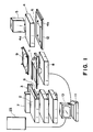
- Figure 1 is a schematic and perspective view of a portion of a semiconductor device manufacturing apparatus according to a first embodiment of the present invention, which portion relates to conveyance of a reticle.
- Figure 2 is a plan view for explaining movement of a reticle in the semiconductor device manufacturing apparatus of the Figure 1 embodiment.
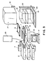
- Figure 3 is a schematic and perspective view of a portion of a semiconductor device manufacturing apparatus according to a second embodiment of the present invention, which portion relates to conveyance of a reticle.
- FIG. 1 denoted in Figure 1 at 6 is a reticle, and denoted at 2 is a reticle cassette for storing a reticle therein.
- a plurality of reticle cassettes 2 can be accommodated.
- Denoted at 7 is a cassette library, and denoted at 3 is a cassette opening/closing mechanism annexed to the cassette library 7.
- Denoted at 5 is a cassette opening/closing mechanism for opening and closing a cassette 4 with an upper cover 4a and a lower base 4b, having a shape different from that of the cassette 2.
- Denoted at 12 is a cassette table on which the cassette 4 can be placed, and denoted at 9 is a reticle stage on which a reticle is to be placed for execution of an exposure process.
- Denoted at 1 is a reticle hand for unloading or loading a reticle out of or into the cassette 2 or the cassette 4, through vacuum attraction.
- Denoted at 8 is reticle hand driving means which serves to perform (i) rotational drive for changing the orientation of the reticle hand 1 toward the cassette 2, the cassette 4 or the reticle stage 9, for example, (ii) horizontal drive for expanding or contracting the reticle hand 1 along a horizontal direction, and (iii) vertical drive for moving the reticle hand upwardly and downwardly.
- Denoted at 11 is control means for controlling the reticle hand driving means 8, the cassette library 7 and the cassette table 12.
- Denoted at 10 is a display for displaying information about the state of operation of the reticle hand as well as the information related to the cassette into which or out of which a reticle has been loaded or unloaded.
- the control means is connected to a superordinate operational unit 23 to which a plurality of semiconductor device manufacturing apparatuses can be connected.
- the cassette 4 of different shape has the same shape as of a cassette to be used in a reticle cleaning apparatus.
- a reticle For use of a reticle in the semiconductor device manufacturing apparatus, an operator loads the cassette 2 having a reticle 6 stored therein into the semiconductor device manufacturing apparatus. Simultaneously therewith, a vacant cassette 4 usable with the cleaning apparatus is loaded. The control means 11 and the display means 10 are manipulated, and the reticle loading operation of the semiconductor device manufacturing apparatus starts. In response, the semiconductor device manufacturing apparatus performs discrimination as to whether there is reticle management information supplied from the operational unit 23, for selection of reticle management information to be used.
- reticle management information supplied from the operational unit 23 it is read into the control means 11. If there is no reticle management information supplied from the operational unit 23, reticle management information having already stored in the apparatus is read into the control means 11.
- control means 11 In response to the reading of the reticle management information, the control means 11 operates to actuate the cassette library 7 to move a designated cassette 2 to the position, the same level as the reticle hand 1, and to open a door of the cassette 2 through the cassette opening/closing mechanism 3.
- the reticle hand 1 As the door of the cassette 2 opens, the reticle hand 1 is rotationally moved toward the cassette 2 and, then, it is moved forwardly into the cassette 2. Subsequently, the reticle hand 1 is moved upwardly so that the reticle 6 within the cassette 2 is placed on the reticle hand 1. Thereafter, the reticle hand 1 holds the reticle 6 in the cassette 2 through vacuum attraction, whereby the reticle 6 is fixedly supported by the reticle hand 1. As the reticle 6 is held by vacuum attraction, the reticle hand 1 is moved backwardly and is rotationally moved toward the reticle stage 9. Then, it is moved forwardly and downwardly and, then, backwardly, whereby the reticle 6 is conveyed onto the reticle stage 9. As a result of this, the reticle 6 is displaced in the direction of an arrow 13 from the position of the cassette 2 in Figure 2, and it is conveyed onto the reticle stage 9.
- the control means 11 rewrites the data, in the reticle management information, regarding the number of operations in which the reticle has been used, to thereby renew that number. If the reticle management information used is the one having been supplied from the superordinate operational unit 23, the renewed reticle management information is transmitted back to the operational unit 23.
- a pattern of the reticle 6 placed on the reticle stage 9 is projected and printed onto a semiconductor wafer (not shown) through the semiconductor device manufacturing apparatus.
- the operator starts the operation for unloading the reticle 6 from the semiconductor device manufacturing apparatus by using the control means 11 and the display 10.
- the control means 11 checks the data, in the reticle management information, regarding the number of operations in which the reticle has been used (i.e., the number of operations in which the reticle has been conveyed onto the reticle stage 9 for execution of the pattern printing process).
- the control means 11 performs the operation reverse to the reticle loading operation, whereby the reticle 6 is collected into the cassette 2 from the reticle stage 9. In response, completion of collection of the reticle 6 into the cassette 2 is displayed by the display 10.
- the motion of the reticle 2 described above corresponds to an arrow 14 in Figure 2, and it means that the reticle 6 is unloaded from the reticle stage 9 into the cassette 2.
- the control means 11 controls the reticle hand 1 to collect the reticle 6 toward the cassette 4 side. More specifically, the reticle hand 1 is rotationally moved toward the reticle stage 9, and then it is moved forwardly and upwardly to hold the reticle 6 through vacuum attraction. Subsequently, the reticle hand 1 is moved backwardly and is rotationally moved toward the cassette 4. As the reticle hand 1 is moved rotationally toward the cassette 4, the cassette opening/closing mechanism 5 opens the upper cover 4a and the lower base 4b of the cassette 4.
- the reticle hand 1 is moved forwardly and downwardly to place the reticle 6 on the lower base 4b. As the reticle 6 is placed on the lower base 4b, the reticle hand 1 moves back and the opening/closing mechanism 5 closes the cassette 4. As the cassette 4 closing motion completes, the display 10 displays information that the reticle 6 has not moved back to the unloaded cassette 2 but it has been collected into the cassette 4. Also, the display 10 displays that the reticle 6 is the one which should be cleaned.
- the reticle 6 is cleaned by the cleaning apparatus (not shown) and, if the operator inputs a command to load the cleaned reticle 6 into the semiconductor device manufacturing apparatus, the cassette 4 unloaded from the reticle cleaning apparatus is placed on the cassette table 12. Also, at the same time, a vacant cassette 2 is set in the cassette library 7.
- the operator manipulates the control means 11 and the display 10 to start the reticle loading operation for loading the reticle into the semiconductor device manufacturing apparatus.
- the semiconductor device manufacturing apparatus checks whether there is reticle management information supplied from the superordinate operational unit 23.
- the reticle management information from the operational unit 23 is read into the control means 11. If there is no reticle management information from the operational unit 23, reticle management information having already stored in the apparatus is read into the control means 11.
- the control means 11 operates to cause the cassette opening/closing driving means 5 of the cassette table 12 to open the upper cover 4a and the lower base 4b of the cassette 4.
- the cassette 4 opens, the reticle hand 1 is rotationally moved toward the cassette 4 and, then, it is moved forwardly and upwardly to hold the reticle 6 by vacuum attraction.
- the reticle hand 1 is moved backwardly and it is moved rotationally toward the reticle stage 9. Subsequently, it is moved forwardly and downwardly, and then, backwardly whereby the reticle 6 is conveyed onto the reticle stage 9.
- the reticle 6 is moved along an arrow 15 from the position of the cassette 4 in Figure 2, and it is conveyed onto the reticle stage 9.
- the control means 11 erases the data, in the reticle management information, concerning the number of operations in which the reticle has been used, and it newly starts management of that number. If the used reticle management information is the one having been supplied from the operational unit 23, the renewed reticle management information is transmitted back to the operational unit 23.
- the operator manipulates the control means 11 and the display 10 to start the operation for unloading the reticle 6 from the semiconductor device manufacturing apparatus.
- the control means 11 checks the data, in the reticle management information, regarding the number of operations in which the reticle has been used.
- the control means 11 performs the operation reverse to the reticle loading operation, by which the reticle 6 is collected into the cassette 2 from the reticle stage 9. Completion of collection of the reticle 6 into the cassette 2 is displayed by the display 10. This operation corresponds to an arrow 14 in Figure 2, and it means that the reticle 6 has been collected into the cassette 2 from the reticle stage 9.
- FIG 3 is a perspective view of a portion of a semiconductor device manufacturing apparatus according to a second embodiment of the present invention, which portion relates to reticle conveyance.
- This embodiment differs from the first embodiment in that: the cassette 4 of different shape shown in Figure 1 is replaced by a cassette 19 which is adapted to accommodate a plurality of reticles 6; and the cassette 4, the cassette table 12 and the cassette opening/closing driving means 5 are replaced by the cassette 19 for plural reticles 6, an upper cassette cover 17 for accommodating the cassette 19, a cassette table 20, and a cassette cover opening/closing mechanism 18.
- the cassette cover opening/closing mechanism 18 serves to open or close a combination of the upper cassette cover 17 and the cassette table 20 on which the cassette 19 is placed.
- the cassette 19 placed on the cassette table 20 is moved by means of an elevator mechanism 22 and a mounting table 21, along a Z direction, namely, upwardly and downwardly.
- the cassette 19 has the same shape as of a cassette used in a reticle particle-inspection apparatus, for example.
- the operator uses a reticle particle-inspection apparatus (not shown) to perform a reticle 6 to be used, in respect to adhesion of foreign particles thereto.
- the reticle 6 having its inspection completed is accommodated in the cassette 19, and the cassette 19 is held on the cassette table 20 and within the upper cassette cover 17.
- the operator mounts the cassette 19, held by the cassette table 20 and the upper cassette cover 17, on the semiconductor device manufacturing apparatus and, at the same time, mounts a vacant cassette 2 which is used as a standard cassette in the semiconductor device manufacturing apparatus. Then, the operator manipulates the control means 11 and the display 10 to start the reticle loading operation of the semiconductor device manufacturing apparatus. In response, the semiconductor device manufacturing apparatus checks, for selection of reticle management information to be used, whether there is reticle management information supplied from the operational unit 23.
- the control means 11 operates to cause the cassette cover opening/closing mechanism 18 to separate the upper cassette cover 17 and the cassette table 20 from each other. This brings the cassette 19 into a state in which it can be separated and moved downwardly.
- the elevator mechanism 22 moves the mounting table 21 downwardly until the position in the cassette 19 where the reticle 6 selected by the operator is placed comes to the same level as of the reticle hand 1.
- the elevator mechanism 21 moves the mounting table 21 to the position of the same level as the reticle hand 1, the reticle hand 1 is moved rotationally toward the cassette 19. Then, it is moved forwardly and upwardly into the cassette 2, so that the reticle hand 1 holds the reticle 6 in the cassette 2 by vacuum attraction. As the reticle 8 is held fixed by vacuum attraction, the reticle hand 1 is moved backwardly and, additionally, it is rotationally moved toward the reticle stage 9. Subsequently, it is moved forwardly and downwardly and, then, backwardly, by which the reticle 6 is conveyed onto the reticle stage 9.
- the reticle 6 is conveyed to the reticle stage 9, from the position of the cassette 12.
- the control means 11 rewrites the data in the reticle management information, related to the reticle 6, and it renews the data regarding the number of operations in which the reticle has been used or the data regarding the apparatus which is going to be used subsequently. If the used reticle management information is the one having been supplied from the operational unit 23, the renewed reticle management information is transmitted back to the operational unit 23.
- the operator Upon completion of use of the reticle 6, for collecting the reticle 6 into the cassette, the operator uses the control unit 11 and the display 10 to start the operation for unloading the reticle 6 out of the semiconductor device manufacturing apparatus.
- the control means 11 checks the data regarding the number of operations in which the reticle has been used or the data regarding the apparatus to be used subsequently.
- control means 11 performs the operation reverse to the reticle loading operation for loading the reticle 6 from the reticle stage 9, such that the reticle 6 is accommodated into the cassette 11, and collection of the reticle 6 into the cassette 11 is displayed by the display 10.
- the reticle 6 is collected from the reticle stage 9 to the cassette 11.
- control means 11 controls the reticle hand 1 to collect the reticle 6 into the cassette 2.
- the reticle hand 1 is rotationally moved toward the reticle stage 9 and, then it is moved forwardly and upwardly into the cassette 2.
- the reticle hand 1 then holds the reticle 6 in the cassette 2 by vacuum attraction, and it is then moved backwardly and rotationally toward the cassette 2.
- the cassette library 7 opens the cassette 2 by using the cassette opening/closing mechanism 3.
- the cassette 2 opens, the reticle hand 1 is moved forwardly and downwardly to place the reticle 6 in the cassette 2.
- the cassette opening/closing mechanism 3 of the cassette library 7 closes the cassette 2.
- the display 10 displays that the reticle is collected into the cassette 2. Also, the display 10 displays the necessity of moving the reticle to a different apparatus.
- the reticle 6 is collected from the reticle stage 9 into the cassette 2.
- the operator places a cassette 2 having been unloaded from the separate apparatus on the cassette library. Also, the operator places the cassette table 20 having the cassette 19 held thereon as well as the upper cassette cover 17, on the mounting table 21.
- the operator manipulates the control means 11 and the display 10 to start the reticle loading operation of the semiconductor device manufacturing apparatus.
- the semiconductor device manufacturing apparatus checks whether there is reticle management information supplied from the operational unit 23.
- the control means 11 moves the cassette 2 in the cassette library 7 to the position of the same level as the reticle hand 1.
- the cassette opening/closing mechanism 5 opens the door of the cassette 2.
- the reticle hand is rotationally moved toward the cassette 2 and, then, it is moved forwardly and upwardly, whereby the reticle is held through vacuum attraction.
- the reticle hand 1 As the reticle is held fixed by vacuum attraction, the reticle hand 1 is moved backward and is moved rotationally toward the reticle stage 9. Subsequently, it is moved forwardly and downwardly and, then, backwardly, whereby the reticle is conveyed onto the reticle stage 9.
- the reticle 6 is conveyed onto the reticle stage 9, from the position of the cassette 2.
- the control means 11 rewrites the data in the reticle management information and renews the data in the reticle management information, regarding the number of operations in which the reticle has been used or the data regarding an apparatus to be used subsequently. If the used reticle management information is the one having been supplied from the operational unit 23, the renewed reticle management information is transmitted back to the operational unit 23.
Landscapes
- Engineering & Computer Science (AREA)
- Physics & Mathematics (AREA)
- General Physics & Mathematics (AREA)
- Condensed Matter Physics & Semiconductors (AREA)
- Manufacturing & Machinery (AREA)
- Computer Hardware Design (AREA)
- Microelectronics & Electronic Packaging (AREA)
- Power Engineering (AREA)
- Library & Information Science (AREA)
- Exposure Of Semiconductors, Excluding Electron Or Ion Beam Exposure (AREA)
- Container, Conveyance, Adherence, Positioning, Of Wafer (AREA)
- Exposure And Positioning Against Photoresist Photosensitive Materials (AREA)
Abstract
Description
- This invention relates generally to a method and apparatus for manufacture of semiconductor devices. More particularly, the invention is concerned with automation of reticle conveyance, for example, in a semiconductor device manufacturing apparatus wherein an original such as a photomask or reticle is to be used.
- In order to prevent adhesion of foreign particles to a reticle, to meet the requirement of further miniaturization of a semiconductor device, semiconductor device manufacturing apparatuses use a mechanism for automatically unloading a reticle from a reticle cassette, which accommodates reticles therein, and for automatically conveying the reticle to an exposure station. Also, in order to avoid adhesion of foreign particles to a reticle, an operator manages the number of operations in which that the reticle is used, to determine execution of a reticle cleaning operation, an inspection operation for adhesion of foreign particles on the reticle, and an inspection operation for any fault of a pattern of the reticle, and so on.
- In such operational environment and apparatus environment, reticle cassettes to be used in a reticle cleaning system, a reticle foreign-particle inspecting system, a reticle pattern-fault inspecting system or the like, have different shapes peculiar to these systems, respectively. There is no unification or compatibility in the shape. For this reason, if a reticle having been cleaned by the reticle cleaning system is to be loaded into the semiconductor device manufacturing apparatus, it is necessary to transfer the reticle from a reticle cassette for the reticle cleaning system into a reticle cassette for the semiconductor device manufacturing apparatus. To this end, the operator carries a reticle cassette having a reticle kept therein and a vacant reticle cassette for the semiconductor device manufacturing apparatus, into a clean room and executes transfer of the reticle between them.
- This necessitates that the operator goes into the clean room every time a reticle is to be transferred. Since the number of reticles to be used is increasing, it causes prolonged work time of the operator for the reticle transfer operations. Also, the manual reticle transfer operation does not avoid particle adhesion completely even if it is done carefully.
- A reticle transfer mechanism has been proposed in an attempt to decreasing the work time and reducing particle adhesion. However, in such mechanism, there is an operation for loading a cassette into which a reticle is to be transferred. Since the cassette has to be loaded manually by an operator, there is a possibility that a reticle which is not to be transferred is transferred by an error of the operator so that the reticle which is not going to be used is loaded into the semiconductor device manufacturing apparatus. If this occurs, the operation of the semiconductor device manufacturing apparatus will be stopped or an erroneous operation will occur.
- Further, the reticle transfer mechanism has to be installed in a clean room. This requires a very large clean room, and it causes increases of cost of the apparatus or settings.
- In is an object of the present invention to provide a method or apparatus for manufacture of semiconductor devices, for example, wherein transfer of an original such as a reticle is executed efficiently while reducing adhesion of foreign particles to the reticle.
- In accordance with an aspect of the present invention, there is provided a semiconductor device manufacturing apparatus, comprising: cassette accommodating means for accommodating a first cassette for storing an original therein; conveying means for unloading the original out of the first cassette in said cassette accommodating means and for conveying the original into said apparatus so that the original is used or processed therein; cassette mounting means for mounting a second cassette having a shape different from that of the first cassette; and conveying means for discriminating whether the original unloaded out of the first cassette, for use or process in said apparatus, is to be moved, after the use or the process, back to the first cassette or the second cassette on the basis of information related to the original and stored in said apparatus, and then for moving the original to one of the first cassette and second cassette.
- Said apparatus may further comprise display means for displaying, to an operator, whether the original is moved to the first cassette or the second cassette.
- Said conveying means may use one of information supplied thereto from an operational unit for controlling said apparatus and information stored in said apparatus, to execute the discrimination.
- In the structure described above, the original unloaded out of the cassette accommodated in said cassette accommodating means may be conveyed to said apparatus and may be used or processed therein.
- Discrimination may be made as to whether the original having been used or processed is to be moved back to the same cassette so that the original is to be used or processed in the same apparatus, or it is to be moved back to a separate cassette, having a different shape, so that the original is to be used in an apparatus for use with the cassette of different shape, wherein discrimination may be made on the basis of selected one of original management information supplied from operational means to control means, for controlling the conveying means, and original management information prepared in said apparatus.
- The original with which the discrimination has been executed may be moved back to an appropriate cassette, in accordance with the original management information selected by an operator.
- After the original is moved back into a cassette in cassette conveying means by said conveying means, the control means may operate to cause display means to perform display, for an operator, concerning the cassette into which the original has been moved back.
- In accordance with this aspect of the present invention, after the original is used or processed, an apparatus which is to be uses subsequently is discriminated automatically without any manual operation or additional mechanism, and the original is transferred automatically to a cassette which is to be used with the subsequent apparatus. This prevents adhesion of particles to the original during the original transfer operation.
- Since the original transfer operation is based on the information within the apparatus, unwanted stoppage of the operation due to an error in original transfer, for example, is avoided. The work time of the operator reduces, and the rate of operation of the apparatus as well as the operation efficiency of the operator increase.
- Embodiments of the present invention will now be described with reference to the accompanying drawings, in which:
- Figure 1 is a schematic and perspective view of a portion of a semiconductor device manufacturing apparatus according to a first embodiment of the present invention, which portion relates to conveyance of a reticle.
- Figure 2 is a plan view for explaining movement of a reticle in the semiconductor device manufacturing apparatus of the Figure 1 embodiment.
- Figure 3 is a schematic and perspective view of a portion of a semiconductor device manufacturing apparatus according to a second embodiment of the present invention, which portion relates to conveyance of a reticle.
- Referring to Figures 1 and 2 showing a semiconductor device manufacturing apparatus according to a first embodiment of the present invention, denoted in Figure 1 at 6 is a reticle, and denoted at 2 is a reticle cassette for storing a reticle therein. In this embodiment, a plurality of
reticle cassettes 2 can be accommodated. Denoted at 7 is a cassette library, and denoted at 3 is a cassette opening/closing mechanism annexed to thecassette library 7. Denoted at 5 is a cassette opening/closing mechanism for opening and closing acassette 4 with anupper cover 4a and alower base 4b, having a shape different from that of thecassette 2. Denoted at 12 is a cassette table on which thecassette 4 can be placed, and denoted at 9 is a reticle stage on which a reticle is to be placed for execution of an exposure process. - Denoted at 1 is a reticle hand for unloading or loading a reticle out of or into the
cassette 2 or thecassette 4, through vacuum attraction. Denoted at 8 is reticle hand driving means which serves to perform (i) rotational drive for changing the orientation of the reticle hand 1 toward thecassette 2, thecassette 4 or thereticle stage 9, for example, (ii) horizontal drive for expanding or contracting the reticle hand 1 along a horizontal direction, and (iii) vertical drive for moving the reticle hand upwardly and downwardly. Denoted at 11 is control means for controlling the reticle hand driving means 8, thecassette library 7 and the cassette table 12. Denoted at 10 is a display for displaying information about the state of operation of the reticle hand as well as the information related to the cassette into which or out of which a reticle has been loaded or unloaded. - The control means is connected to a superordinate
operational unit 23 to which a plurality of semiconductor device manufacturing apparatuses can be connected. Thecassette 4 of different shape has the same shape as of a cassette to be used in a reticle cleaning apparatus. - The operation of the apparatus will be described with reference to Figures 1 and 2.
- For use of a reticle in the semiconductor device manufacturing apparatus, an operator loads the
cassette 2 having areticle 6 stored therein into the semiconductor device manufacturing apparatus. Simultaneously therewith, avacant cassette 4 usable with the cleaning apparatus is loaded. The control means 11 and the display means 10 are manipulated, and the reticle loading operation of the semiconductor device manufacturing apparatus starts. In response, the semiconductor device manufacturing apparatus performs discrimination as to whether there is reticle management information supplied from theoperational unit 23, for selection of reticle management information to be used. - If there is reticle management information supplied from the
operational unit 23, it is read into the control means 11. If there is no reticle management information supplied from theoperational unit 23, reticle management information having already stored in the apparatus is read into the control means 11. - In response to the reading of the reticle management information, the control means 11 operates to actuate the
cassette library 7 to move a designatedcassette 2 to the position, the same level as the reticle hand 1, and to open a door of thecassette 2 through the cassette opening/closing mechanism 3. - As the door of the
cassette 2 opens, the reticle hand 1 is rotationally moved toward thecassette 2 and, then, it is moved forwardly into thecassette 2. Subsequently, the reticle hand 1 is moved upwardly so that thereticle 6 within thecassette 2 is placed on the reticle hand 1. Thereafter, the reticle hand 1 holds thereticle 6 in thecassette 2 through vacuum attraction, whereby thereticle 6 is fixedly supported by the reticle hand 1. As thereticle 6 is held by vacuum attraction, the reticle hand 1 is moved backwardly and is rotationally moved toward thereticle stage 9. Then, it is moved forwardly and downwardly and, then, backwardly, whereby thereticle 6 is conveyed onto thereticle stage 9. As a result of this, thereticle 6 is displaced in the direction of anarrow 13 from the position of thecassette 2 in Figure 2, and it is conveyed onto thereticle stage 9. - As the
reticle 6 is conveyed onto thereticle stage 9, the control means 11 rewrites the data, in the reticle management information, regarding the number of operations in which the reticle has been used, to thereby renew that number. If the reticle management information used is the one having been supplied from the superordinateoperational unit 23, the renewed reticle management information is transmitted back to theoperational unit 23. - A pattern of the
reticle 6 placed on thereticle stage 9 is projected and printed onto a semiconductor wafer (not shown) through the semiconductor device manufacturing apparatus. When a predetermined exposure process or processes are completed and the use of thereticle 6 is to be finished, for collection of thereticle 6 into thecassette 2, the operator starts the operation for unloading thereticle 6 from the semiconductor device manufacturing apparatus by using the control means 11 and thedisplay 10. In response, the control means 11 checks the data, in the reticle management information, regarding the number of operations in which the reticle has been used (i.e., the number of operations in which the reticle has been conveyed onto thereticle stage 9 for execution of the pattern printing process). - If this number is less than a predetermined limitation number for use of the reticle, the control means 11 performs the operation reverse to the reticle loading operation, whereby the
reticle 6 is collected into thecassette 2 from thereticle stage 9. In response, completion of collection of thereticle 6 into thecassette 2 is displayed by thedisplay 10. The motion of thereticle 2 described above corresponds to anarrow 14 in Figure 2, and it means that thereticle 6 is unloaded from thereticle stage 9 into thecassette 2. - If the data in the reticle management information, concerning the number of operations in which the reticle has been used, is equal to the predetermined limitation number, the control means 11 controls the reticle hand 1 to collect the
reticle 6 toward thecassette 4 side. More specifically, the reticle hand 1 is rotationally moved toward thereticle stage 9, and then it is moved forwardly and upwardly to hold thereticle 6 through vacuum attraction. Subsequently, the reticle hand 1 is moved backwardly and is rotationally moved toward thecassette 4. As the reticle hand 1 is moved rotationally toward thecassette 4, the cassette opening/closing mechanism 5 opens theupper cover 4a and thelower base 4b of thecassette 4. After thecassette 4 is opened, the reticle hand 1 is moved forwardly and downwardly to place thereticle 6 on thelower base 4b. As thereticle 6 is placed on thelower base 4b, the reticle hand 1 moves back and the opening/closing mechanism 5 closes thecassette 4. As thecassette 4 closing motion completes, thedisplay 10 displays information that thereticle 6 has not moved back to the unloadedcassette 2 but it has been collected into thecassette 4. Also, thedisplay 10 displays that thereticle 6 is the one which should be cleaned. - The operation described above corresponds to an
arrow 16 in Figure 2, and it means that thereticle 6 has been unloaded from thereticle stage 9 into thecassette 4. - The
reticle 6 is cleaned by the cleaning apparatus (not shown) and, if the operator inputs a command to load the cleanedreticle 6 into the semiconductor device manufacturing apparatus, thecassette 4 unloaded from the reticle cleaning apparatus is placed on the cassette table 12. Also, at the same time, avacant cassette 2 is set in thecassette library 7. - After these cassettes are set in the semiconductor device manufacturing apparatus, the operator manipulates the control means 11 and the
display 10 to start the reticle loading operation for loading the reticle into the semiconductor device manufacturing apparatus. In response, for selection of reticle management information to be used, the semiconductor device manufacturing apparatus checks whether there is reticle management information supplied from the superordinateoperational unit 23. - If there is reticle management information supplied from the
operational unit 23, the reticle management information from theoperational unit 23 is read into the control means 11. If there is no reticle management information from theoperational unit 23, reticle management information having already stored in the apparatus is read into the control means 11. - As the reticle management information is read, the control means 11 operates to cause the cassette opening/closing driving means 5 of the cassette table 12 to open the
upper cover 4a and thelower base 4b of thecassette 4. As thecassette 4 opens, the reticle hand 1 is rotationally moved toward thecassette 4 and, then, it is moved forwardly and upwardly to hold thereticle 6 by vacuum attraction. - As the
reticle 6 is held fixed by vacuum attraction, the reticle hand 1 is moved backwardly and it is moved rotationally toward thereticle stage 9. Subsequently, it is moved forwardly and downwardly, and then, backwardly whereby thereticle 6 is conveyed onto thereticle stage 9. - With this operation, the
reticle 6 is moved along anarrow 15 from the position of thecassette 4 in Figure 2, and it is conveyed onto thereticle stage 9. - As the
reticle 6 is conveyed onto thereticle stage 9, the control means 11 erases the data, in the reticle management information, concerning the number of operations in which the reticle has been used, and it newly starts management of that number. If the used reticle management information is the one having been supplied from theoperational unit 23, the renewed reticle management information is transmitted back to theoperational unit 23. - After the
reticle 6 is used so that it is to be collected back to a cassette, the operator manipulates the control means 11 and thedisplay 10 to start the operation for unloading thereticle 6 from the semiconductor device manufacturing apparatus. In response, the control means 11 checks the data, in the reticle management information, regarding the number of operations in which the reticle has been used. - If this number is less than a predetermined limitation number for use of the reticle, the control means 11 performs the operation reverse to the reticle loading operation, by which the
reticle 6 is collected into thecassette 2 from thereticle stage 9. Completion of collection of thereticle 6 into thecassette 2 is displayed by thedisplay 10. This operation corresponds to anarrow 14 in Figure 2, and it means that thereticle 6 has been collected into thecassette 2 from thereticle stage 9. - Figure 3 is a perspective view of a portion of a semiconductor device manufacturing apparatus according to a second embodiment of the present invention, which portion relates to reticle conveyance. This embodiment differs from the first embodiment in that: the
cassette 4 of different shape shown in Figure 1 is replaced by acassette 19 which is adapted to accommodate a plurality ofreticles 6; and thecassette 4, the cassette table 12 and the cassette opening/closing driving means 5 are replaced by thecassette 19 forplural reticles 6, anupper cassette cover 17 for accommodating thecassette 19, a cassette table 20, and a cassette cover opening/closing mechanism 18. The cassette cover opening/closing mechanism 18 serves to open or close a combination of theupper cassette cover 17 and the cassette table 20 on which thecassette 19 is placed. - The
cassette 19 placed on the cassette table 20 is moved by means of anelevator mechanism 22 and a mounting table 21, along a Z direction, namely, upwardly and downwardly. - The
cassette 19 has the same shape as of a cassette used in a reticle particle-inspection apparatus, for example. - The operation of the semiconductor device manufacturing apparatus of this embodiment will be explained with reference to Figure 3.
- When a reticle is going to be used in the semiconductor device manufacturing apparatus, the operator uses a reticle particle-inspection apparatus (not shown) to perform a
reticle 6 to be used, in respect to adhesion of foreign particles thereto. Thereticle 6 having its inspection completed is accommodated in thecassette 19, and thecassette 19 is held on the cassette table 20 and within theupper cassette cover 17. - The operator mounts the
cassette 19, held by the cassette table 20 and theupper cassette cover 17, on the semiconductor device manufacturing apparatus and, at the same time, mounts avacant cassette 2 which is used as a standard cassette in the semiconductor device manufacturing apparatus. Then, the operator manipulates the control means 11 and thedisplay 10 to start the reticle loading operation of the semiconductor device manufacturing apparatus. In response, the semiconductor device manufacturing apparatus checks, for selection of reticle management information to be used, whether there is reticle management information supplied from theoperational unit 23. - If there is reticle management information supplied from the
operational unit 23, it is read into the control means 11. If there is no reticle management information supplied from theoperational unit 23, the reticle management information having already stored in the apparatus is read into the control means 11. - As the reticle management information is read, the control means 11 operates to cause the cassette cover opening/
closing mechanism 18 to separate theupper cassette cover 17 and the cassette table 20 from each other. This brings thecassette 19 into a state in which it can be separated and moved downwardly. - As the
cassette 19 is brought into a state in which it can be separated and moved downwardly, theelevator mechanism 22 moves the mounting table 21 downwardly until the position in thecassette 19 where thereticle 6 selected by the operator is placed comes to the same level as of the reticle hand 1. - As the
elevator mechanism 21 moves the mounting table 21 to the position of the same level as the reticle hand 1, the reticle hand 1 is moved rotationally toward thecassette 19. Then, it is moved forwardly and upwardly into thecassette 2, so that the reticle hand 1 holds thereticle 6 in thecassette 2 by vacuum attraction. As thereticle 8 is held fixed by vacuum attraction, the reticle hand 1 is moved backwardly and, additionally, it is rotationally moved toward thereticle stage 9. Subsequently, it is moved forwardly and downwardly and, then, backwardly, by which thereticle 6 is conveyed onto thereticle stage 9. - With this operation, the
reticle 6 is conveyed to thereticle stage 9, from the position of thecassette 12. - As the
reticle 6 is conveyed onto thereticle stage 9, the control means 11 rewrites the data in the reticle management information, related to thereticle 6, and it renews the data regarding the number of operations in which the reticle has been used or the data regarding the apparatus which is going to be used subsequently. If the used reticle management information is the one having been supplied from theoperational unit 23, the renewed reticle management information is transmitted back to theoperational unit 23. - Upon completion of use of the
reticle 6, for collecting thereticle 6 into the cassette, the operator uses the control unit 11 and thedisplay 10 to start the operation for unloading thereticle 6 out of the semiconductor device manufacturing apparatus. In response, the control means 11 checks the data regarding the number of operations in which the reticle has been used or the data regarding the apparatus to be used subsequently. - If, in relation to use of the
reticle 6, the same apparatus is to be used again, the control means 11 performs the operation reverse to the reticle loading operation for loading thereticle 6 from thereticle stage 9, such that thereticle 6 is accommodated into the cassette 11, and collection of thereticle 6 into the cassette 11 is displayed by thedisplay 10. - With this operation, the
reticle 6 is collected from thereticle stage 9 to the cassette 11. - If a different apparatus is to be used subsequently, the control means 11 controls the reticle hand 1 to collect the
reticle 6 into thecassette 2. - More specifically, the reticle hand 1 is rotationally moved toward the
reticle stage 9 and, then it is moved forwardly and upwardly into thecassette 2. The reticle hand 1 then holds thereticle 6 in thecassette 2 by vacuum attraction, and it is then moved backwardly and rotationally toward thecassette 2. - As the reticle hand 1 is rotationally moved toward the
cassette 2, thecassette library 7 opens thecassette 2 by using the cassette opening/closing mechanism 3. As thecassette 2 opens, the reticle hand 1 is moved forwardly and downwardly to place thereticle 6 in thecassette 2. As thereticle 6 is placed in thecassette 2, the reticle hand 1 moves backwardly. As the reticle hand 1 moves backwardly, the cassette opening/closing mechanism 3 of thecassette library 7 closes thecassette 2. As thecassette 2 closes, thereticle 6 does not move back to thecassette 19 from which thereticle 6 has been unloaded, and thedisplay 10 displays that the reticle is collected into thecassette 2. Also, thedisplay 10 displays the necessity of moving the reticle to a different apparatus. - With this operation, the
reticle 6 is collected from thereticle stage 9 into thecassette 2. - If a
reticle 6 having been unloaded from a separate apparatus is to be loaded into the semiconductor device manufacturing apparatus, the operator places acassette 2 having been unloaded from the separate apparatus on the cassette library. Also, the operator places the cassette table 20 having thecassette 19 held thereon as well as theupper cassette cover 17, on the mounting table 21. - After these cassettes are set in the semiconductor device manufacturing apparatus, the operator manipulates the control means 11 and the
display 10 to start the reticle loading operation of the semiconductor device manufacturing apparatus. In response, for selection of reticle management information to be used, the semiconductor device manufacturing apparatus checks whether there is reticle management information supplied from theoperational unit 23. - If there is reticle management information supplied from the
operational unit 23, it is read into the control means 11. If there is no reticle management information supplied from theoperational unit 23, the reticle management information having already stored in the apparatus is read into the control unit 11. - As the reticle management information is read, the control means 11 moves the
cassette 2 in thecassette library 7 to the position of the same level as the reticle hand 1. As thecassette 2 is moved up to this position, the cassette opening/closing mechanism 5 opens the door of thecassette 2. As the door of thecassette 2 opens, the reticle hand is rotationally moved toward thecassette 2 and, then, it is moved forwardly and upwardly, whereby the reticle is held through vacuum attraction. - As the reticle is held fixed by vacuum attraction, the reticle hand 1 is moved backward and is moved rotationally toward the
reticle stage 9. Subsequently, it is moved forwardly and downwardly and, then, backwardly, whereby the reticle is conveyed onto thereticle stage 9. - With this operation, the
reticle 6 is conveyed onto thereticle stage 9, from the position of thecassette 2. - As the
reticle 6 is conveyed onto thereticle stage 9, the control means 11 rewrites the data in the reticle management information and renews the data in the reticle management information, regarding the number of operations in which the reticle has been used or the data regarding an apparatus to be used subsequently. If the used reticle management information is the one having been supplied from theoperational unit 23, the renewed reticle management information is transmitted back to theoperational unit 23. - While the invention has been described with reference to the structures disclosed herein, it is not confined to the details set forth and this application is intended to cover such modifications or changes as may come within the purposes of the improvements or the scope of the following claims.
Claims (12)
- A semiconductor device manufacturing apparatus, comprising:cassette accommodating means for accommodating a first cassette for storing an original therein;conveying means for unloading the original out of the first cassette in said cassette accommodating means and for conveying the original into said apparatus so that the original is used or processed therein;cassette mounting means for mounting a second cassette having a shape different from that of the first cassette; andconveying means for discriminating whether the original unloaded out of the first cassette, for use or process in said apparatus, is to be moved, after the use or the process, back to the first cassette or the second cassette on the basis of information related to the original and stored in said apparatus, and then for moving the original to one of the first cassette and second cassette.
- An apparatus according to Claim 1, further comprising display means for displaying, to an operator, whether the original is moved to the first cassette or the second cassette.
- An apparatus according to Claim 1, wherein said conveying means uses one of information supplied thereto from an operational unit for controlling said apparatus and information stored in said apparatus, to execute the discrimination.
- A semiconductor device manufacturing method, comprising the steps of:unloading a reticle out of a first cassette accommodated in first cassette accommodating means and placing the reticle on a reticle stage;executing a process for semiconductor device manufacture by using the reticle placed on the reticle stage;collecting, after the execution, the reticle on the reticle stage;discriminating, through control means, whether the reticle is to be moved back to the first cassette or to a second cassette having a shape different from that of the first cassette, on the basis of information stored in the control means; andconveying, through conveying means, the reticle to one of the first and second cassettes in accordance with the discrimination.
- A method according to Claim 4, wherein the control means performs the discrimination on the basis of the number of operations of conveyance and use of the reticle on the reticle stage.
- A method according to Claim 5, further comprising cleaning the reticle, as conveyed into the second cassette, outside the second cassette.
- A method according to Claim 6, wherein the second cassette is adapted to accommodate plural reticles therein.
- A semiconductor device manufacturing method comprising the steps of:unloading an original from a first cassette storage means;placing the original on an original stage;executing a process for semiconductor manufacture using the original;collecting the original from the original stage;determining whether the original has been used for a threshold number of process executions;returning the original to the first cassette storage means if the original has been used for less than the threshold number of process executions, or placing the original in a second cassette storage means if the original has been used for less than the threshold number of process executions.
- A method according to claim 8, wherein cleaning of the original takes place in the second cassette storage means.
- A method according to claim 8 or claim 9, wherein the process comprises exposure of a substrate through the original to print a semiconductor device pattern on the substrate.
- A semiconductor device manufacturing apparatus comprising:first cassette storage means for storing an original therein;second cassette storage means for storing an original therein;conveying means for unloading an original from the first cassette storage means for use in a process for semiconductor manufacture using the original, and for returning the original to the first cassette storage means or placing the original in the second storage means in dependence upon whether the original has been used for respectively less or more than a threshold number of process executions.
- Apparatus according to claim 11, wherein the second cassette storage means comprises an original cleaning stage where cleaning of the original takes place.
Applications Claiming Priority (3)
| Application Number | Priority Date | Filing Date | Title |
|---|---|---|---|
| JP14686895 | 1995-05-23 | ||
| JP14686895A JP3347528B2 (en) | 1995-05-23 | 1995-05-23 | Semiconductor manufacturing equipment |
| JP146868/95 | 1995-05-23 |
Publications (3)
| Publication Number | Publication Date |
|---|---|
| EP0744764A2 true EP0744764A2 (en) | 1996-11-27 |
| EP0744764A3 EP0744764A3 (en) | 1997-11-12 |
| EP0744764B1 EP0744764B1 (en) | 2005-03-02 |
Family
ID=15417389
Family Applications (1)
| Application Number | Title | Priority Date | Filing Date |
|---|---|---|---|
| EP96303562A Expired - Lifetime EP0744764B1 (en) | 1995-05-23 | 1996-05-20 | Method and apparatus for manufacture of semiconductor devices |
Country Status (5)
| Country | Link |
|---|---|
| US (1) | US5740052A (en) |
| EP (1) | EP0744764B1 (en) |
| JP (1) | JP3347528B2 (en) |
| KR (1) | KR100193154B1 (en) |
| DE (1) | DE69634395D1 (en) |
Cited By (2)
| Publication number | Priority date | Publication date | Assignee | Title |
|---|---|---|---|---|
| EP0940721A2 (en) * | 1998-03-04 | 1999-09-08 | Hewlett-Packard Company | Reticle library apparatus and method |
| EP1043625A1 (en) * | 1997-12-25 | 2000-10-11 | Nikon Corporation | Method and apparatus for manufacturing photomask and method of fabricating device |
Families Citing this family (8)
| Publication number | Priority date | Publication date | Assignee | Title |
|---|---|---|---|---|
| JPH0936198A (en) * | 1995-07-19 | 1997-02-07 | Hitachi Ltd | Vacuum processor and semiconductor production line using the processor |
| JP3741401B2 (en) | 1998-02-27 | 2006-02-01 | キヤノン株式会社 | Substrate transport device, semiconductor manufacturing device, and liquid crystal plate manufacturing device |
| US6136614A (en) * | 1998-03-04 | 2000-10-24 | Agilent Technologies | Apparatus and method for manufacturing integrated circuit devices |
| US6192290B1 (en) * | 1998-05-21 | 2001-02-20 | Lucent Technologies Inc. | System and method of manufacturing semicustom integrated circuits using reticle primitives from a library and interconnect reticles |
| JP3513437B2 (en) | 1999-09-01 | 2004-03-31 | キヤノン株式会社 | Substrate management method and semiconductor exposure apparatus |
| US6746879B1 (en) * | 2002-10-02 | 2004-06-08 | Taiwan Semiconductor Manufacturing Company | Guard filter methodology and automation system to avoid scrap due to reticle errors |
| JP2004228474A (en) * | 2003-01-27 | 2004-08-12 | Canon Inc | Original-edition conveyor |
| US7206652B2 (en) * | 2004-08-20 | 2007-04-17 | International Business Machines Corporation | Method and system for intelligent automated reticle management |
Citations (1)
| Publication number | Priority date | Publication date | Assignee | Title |
|---|---|---|---|---|
| US4676637A (en) * | 1984-10-24 | 1987-06-30 | Hitachi, Ltd. | Exposure apparatus with foreign particle detector |
Family Cites Families (12)
| Publication number | Priority date | Publication date | Assignee | Title |
|---|---|---|---|---|
| US4062463A (en) * | 1976-05-11 | 1977-12-13 | Machine Technology, Inc. | Automated single cassette load mechanism for scrubber |
| JPS598352Y2 (en) * | 1979-05-28 | 1984-03-15 | 富士通株式会社 | Glass mask cleaning equipment |
| US4248508A (en) * | 1979-08-03 | 1981-02-03 | The Perkin-Elmer Corporation | Projection mask storage and carrier system |
| US4549843A (en) * | 1983-03-15 | 1985-10-29 | Micronix Partners | Mask loading apparatus, method and cassette |
| US4758127A (en) * | 1983-06-24 | 1988-07-19 | Canon Kabushiki Kaisha | Original feeding apparatus and a cassette for containing the original |
| US5097421A (en) * | 1984-12-24 | 1992-03-17 | Asyst Technologies, Inc. | Intelligent waxer carrier |
| US4757355A (en) * | 1985-10-29 | 1988-07-12 | Canon Kabushiki Kaisha | Mask storing mechanism |
| US4746256A (en) * | 1986-03-13 | 1988-05-24 | Roboptek, Inc. | Apparatus for handling sensitive material such as semiconductor wafers |
| US4999671A (en) * | 1986-07-11 | 1991-03-12 | Canon Kabushiki Kaisha | Reticle conveying device |
| US4984953A (en) * | 1987-02-20 | 1991-01-15 | Canon Kabushiki Kaisha | Plate-like article conveying system |
| EP0358443B1 (en) * | 1988-09-06 | 1997-11-26 | Canon Kabushiki Kaisha | Mask cassette loading device |
| JPH0758397B2 (en) * | 1989-12-05 | 1995-06-21 | 株式会社東芝 | Mask management device |
-
1995
- 1995-05-23 JP JP14686895A patent/JP3347528B2/en not_active Expired - Fee Related
-
1996
- 1996-05-17 US US08/651,038 patent/US5740052A/en not_active Expired - Lifetime
- 1996-05-20 DE DE69634395T patent/DE69634395D1/en not_active Expired - Lifetime
- 1996-05-20 EP EP96303562A patent/EP0744764B1/en not_active Expired - Lifetime
- 1996-05-23 KR KR1019960017605A patent/KR100193154B1/en not_active IP Right Cessation
Patent Citations (1)
| Publication number | Priority date | Publication date | Assignee | Title |
|---|---|---|---|---|
| US4676637A (en) * | 1984-10-24 | 1987-06-30 | Hitachi, Ltd. | Exposure apparatus with foreign particle detector |
Cited By (4)
| Publication number | Priority date | Publication date | Assignee | Title |
|---|---|---|---|---|
| EP1043625A1 (en) * | 1997-12-25 | 2000-10-11 | Nikon Corporation | Method and apparatus for manufacturing photomask and method of fabricating device |
| EP1043625A4 (en) * | 1997-12-25 | 2004-11-10 | Nikon Corp | Method and apparatus for manufacturing photomask and method of fabricating device |
| EP0940721A2 (en) * | 1998-03-04 | 1999-09-08 | Hewlett-Packard Company | Reticle library apparatus and method |
| EP0940721A3 (en) * | 1998-03-04 | 2003-03-12 | Agilent Technologies, Inc. (a Delaware corporation) | Reticle library apparatus and method |
Also Published As
| Publication number | Publication date |
|---|---|
| JP3347528B2 (en) | 2002-11-20 |
| EP0744764B1 (en) | 2005-03-02 |
| KR960042919A (en) | 1996-12-21 |
| JPH08316137A (en) | 1996-11-29 |
| KR100193154B1 (en) | 1999-06-15 |
| US5740052A (en) | 1998-04-14 |
| EP0744764A3 (en) | 1997-11-12 |
| DE69634395D1 (en) | 2005-04-07 |
Similar Documents
| Publication | Publication Date | Title |
|---|---|---|
| US5740052A (en) | Method and apparatus for manufacture of semiconductor devices | |
| US7778721B2 (en) | Small lot size lithography bays | |
| KR20010034647A (en) | Cluster tool | |
| EP0756316A1 (en) | Vacuum processing apparatus and semiconductor manufacturing line using the same | |
| US6398476B1 (en) | Automatic storage unit and automatic storing method | |
| US6772032B2 (en) | Semiconductor device manufacturing line | |
| US6457587B1 (en) | Integrated reticle sorter and stocker | |
| JP2010509785A (en) | Removable compartment for workpiece stocker | |
| JP2791251B2 (en) | Semiconductor processing apparatus and method, and semiconductor processing apparatus module | |
| US6618639B2 (en) | System, process, apparatus and program for controlling special lot carrying in semiconductor carrying facility | |
| US6945258B2 (en) | Substrate processing apparatus and method | |
| US20020003994A1 (en) | Component source interchange gantry | |
| JP5160603B2 (en) | Substrate processing apparatus, substrate processing method, and storage medium | |
| US6392403B1 (en) | Integrated wafer stocker and sorter apparatus | |
| JPH09260461A (en) | Semiconductor manufacture device | |
| KR100370635B1 (en) | METHOD AND APPARATUS CONTROL METHOD | |
| JP2002270669A (en) | Substrate transfer method and apparatus | |
| US6057697A (en) | Measurement system for a semiconductor manufacturing line in which a robot conveys wafers among a cluster of checking parts | |
| EP0940721A2 (en) | Reticle library apparatus and method | |
| JPH11147613A (en) | Original edition conveyer device | |
| JPH10198585A (en) | Controller | |
| JP4056284B2 (en) | Substrate processing apparatus and substrate processing method | |
| JP2774911B2 (en) | Semiconductor wafer transfer device | |
| JPS6322410A (en) | Printed circuit board accommodating rack | |
| JPH08181057A (en) | Exposure apparatus and method therefor |
Legal Events
| Date | Code | Title | Description |
|---|---|---|---|
| PUAI | Public reference made under article 153(3) epc to a published international application that has entered the european phase |
Free format text: ORIGINAL CODE: 0009012 |
|
| AK | Designated contracting states |
Kind code of ref document: A2 Designated state(s): DE GB NL |
|
| PUAL | Search report despatched |
Free format text: ORIGINAL CODE: 0009013 |
|
| AK | Designated contracting states |
Kind code of ref document: A3 Designated state(s): DE GB NL |
|
| 17P | Request for examination filed |
Effective date: 19980325 |
|
| 17Q | First examination report despatched |
Effective date: 20000814 |
|
| GRAP | Despatch of communication of intention to grant a patent |
Free format text: ORIGINAL CODE: EPIDOSNIGR1 |
|
| RIN1 | Information on inventor provided before grant (corrected) |
Inventor name: NAKAMURA, GEN,C/O KOSUGI JIGYOSHO CANON K. K. |
|
| GRAS | Grant fee paid |
Free format text: ORIGINAL CODE: EPIDOSNIGR3 |
|
| GRAA | (expected) grant |
Free format text: ORIGINAL CODE: 0009210 |
|
| AK | Designated contracting states |
Kind code of ref document: B1 Designated state(s): DE GB NL |
|
| PG25 | Lapsed in a contracting state [announced via postgrant information from national office to epo] |
Ref country code: NL Free format text: LAPSE BECAUSE OF FAILURE TO SUBMIT A TRANSLATION OF THE DESCRIPTION OR TO PAY THE FEE WITHIN THE PRESCRIBED TIME-LIMIT Effective date: 20050302 |
|
| REG | Reference to a national code |
Ref country code: GB Ref legal event code: FG4D |
|
| REF | Corresponds to: |
Ref document number: 69634395 Country of ref document: DE Date of ref document: 20050407 Kind code of ref document: P |
|
| PG25 | Lapsed in a contracting state [announced via postgrant information from national office to epo] |
Ref country code: DE Free format text: LAPSE BECAUSE OF FAILURE TO SUBMIT A TRANSLATION OF THE DESCRIPTION OR TO PAY THE FEE WITHIN THE PRESCRIBED TIME-LIMIT Effective date: 20050603 |
|
| NLV1 | Nl: lapsed or annulled due to failure to fulfill the requirements of art. 29p and 29m of the patents act | ||
| PLBE | No opposition filed within time limit |
Free format text: ORIGINAL CODE: 0009261 |
|
| STAA | Information on the status of an ep patent application or granted ep patent |
Free format text: STATUS: NO OPPOSITION FILED WITHIN TIME LIMIT |
|
| 26N | No opposition filed |
Effective date: 20051205 |
|
| PGFP | Annual fee paid to national office [announced via postgrant information from national office to epo] |
Ref country code: GB Payment date: 20140523 Year of fee payment: 19 |
|
| GBPC | Gb: european patent ceased through non-payment of renewal fee |
Effective date: 20150520 |
|
| PG25 | Lapsed in a contracting state [announced via postgrant information from national office to epo] |
Ref country code: GB Free format text: LAPSE BECAUSE OF NON-PAYMENT OF DUE FEES Effective date: 20150520 |