EP0741350B1 - Switch capacitor interface circuit - Google Patents
Switch capacitor interface circuit Download PDFInfo
- Publication number
- EP0741350B1 EP0741350B1 EP96303060A EP96303060A EP0741350B1 EP 0741350 B1 EP0741350 B1 EP 0741350B1 EP 96303060 A EP96303060 A EP 96303060A EP 96303060 A EP96303060 A EP 96303060A EP 0741350 B1 EP0741350 B1 EP 0741350B1
- Authority
- EP
- European Patent Office
- Prior art keywords
- voltage
- terminal
- mosfet switch
- circuit
- switch
- Prior art date
- Legal status (The legal status is an assumption and is not a legal conclusion. Google has not performed a legal analysis and makes no representation as to the accuracy of the status listed.)
- Expired - Lifetime
Links
Images

Classifications
-
- G—PHYSICS
- G01—MEASURING; TESTING
- G01R—MEASURING ELECTRIC VARIABLES; MEASURING MAGNETIC VARIABLES
- G01R19/00—Arrangements for measuring currents or voltages or for indicating presence or sign thereof
Definitions
- the present invention relates generally to an interface circuit connected between a processing component and a sensor. More specifically, the invention relates to an interface circuit that translates sensor voltages outside the voltage range of the power supply voltage of the processing component into voltages within range of the power supply voltage of the processing component.
- Sensors particularly in automotive applications, produce varying output voltages corresponding to particular sensed characteristics.
- the output of a sensor usually requires signal processing such as noise filtering and analogue-to-digital conversion, for example.
- Signal processing circuits commonly use CMOS components having a zero to five volt power supply. It is common for sensors to produce an output voltage exceeding the range of the power supply of the CMOS circuitry. Voltages exceeding the power supply voltage result in an inaccurate measurement. Consequently, some interface circuit is required to translate the sensor voltage within the range of the power supply.
- Previous voltage translation circuits use a MOS type transistor to perform switching of the sensor output voltages across a pair of capacitors according to a clock signal.
- This type of circuit is known as a switched capacitor circuit.
- this voltage translation circuitry does not take into account high voltages which may be developed at the switch.
- MOS type transistors have a gate terminal which is isolated from a drain terminal, a source terminal and bulk terminal by a gate oxide layer. The gate oxide layer must be thick enough to withstand excessive voltage potentials generated during the switching of the transistor. Sudden failure of the transistor due to extremely excessive voltages is an eventuality that must be taken into account by the design.
- Time dependent dielectric breakdown is another type of failure that occurs when the MOS type transistor breaks down over time due to the stress of excessive voltages across the gate oxide layer.
- the gate oxide layer of prior designs is formed thick enough (e.g., at least 250 angstroms thick) to withstand the relatively high voltage potentials developed during switching.
- US-A-4 716 319 describes a MOS switched capacitor integrated circuit configuration for use in low voltage supply applications.
- the circuit configuration has a reference supply node, an operational amplifier having an inverting input terminal, a non inverting input terminal connected to the reference node and an output terminal connected to the integrated circuit output node.
- a capacitor has first and second plates, the second plate being coupled to the operational amplifier inverting input terminal.
- An N-channel MOS transistor receiving a first control signal constitutes a first switch connected between the integrated circuit input node and the first capacitor plate.
- An N-channel MOS transistor receiving a second control signal constitutes a second switch between the first capacitor plate and the reference node and an N-channel MOS transistor receiving a third control signal constitutes a third switch connected to the operational amplifier input terminal.
- Clock signals provide the control signals to each of the switches.
- the first and second control signals are delayed with respect to the third control signal whereby adverse switching characteristics of the first and second switches do not affect the charge injection at the operational amplifier inverting input terminal
- US-A-5 210 501 describes a circuit arrangement for processing the output from a sensor such as a resistance sensor.
- the processing circuit converts the sensor signal to an output signal of a desired form preferably related to a reference signal.
- the processing circuit includes a buffer and an integrating circuit.
- the buffer includes a first operational amplifier, a first storage capacitor and two switches. When the first switch is closed it connects the output of the first amplifier to an inverting input thereof. When the second switch is closed it connects the output of the first amplifier to the one electrode of the first storage capacitor the other of which is connected to the inverting input of the first operational amplifier so that the first storage capacitor lies in the feedback path of the first operational amplifier.
- the integrator includes a second operational amplifier, an integration capacitor lying in the feedback path of this second operational amplifier and a switch operable to close a connection between the inverting input of the second operational amplifier and the first storage capacitor.
- the analog output signal is proportional to the measurement result from the sensor.
- CMOS processes have been developed using thinner gate oxide thickness (e.g., 150 angstroms or less). Components using reduced oxide gate thickness are cheaper to manufacture, have faster switching times and have a smaller package size, all of which are desirable in integrated circuit designs. Previous voltage translation circuits generate high gate oxide voltages which would cause TDDB if thinner CMOS gate oxides were used.
- One advantage of the circuit is that accurate voltage translation has been accomplished while controlling the operating voltages of the MOS transistors used within the circuit.
- the present invention is an interface circuit connecting a sensor to a switched capacitor circuit.
- the switched capacitor circuit is connected to a processing component having a power supply voltage range.
- the sensor has an output voltage range outside the voltage range of the power supply.
- the interface circuit includes a MOSFET switch connected between the sensor and the switched capacitor circuit for connecting the output voltage to the switched capacitor circuit.
- the MOSFET switch has a gate oxide layer, a switch conducting state resistance, a gate voltage and bulk voltage.
- a control circuit is connected to the output of the sensor and to the MOSFET switch and continually adjusts the gate voltage and the bulk voltage in relation to the output voltage to prevent a voltage across the gate oxide layer from exceeding a predetermined value corresponding to time dependent dielectric breakdown.
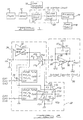
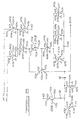
- automobiles have components such as an engine 10 requiring sensed operating parameters to be input to a processing circuit 14 such as an engine control module.
- Processing circuit 14 adjusts the operating parameters of engine 10 accordingly.
- a sensor 12 connected to some portion of engine 10 converts a monitored operating condition such as mass air flow into a corresponding electrical signal.
- Processing circuit 14 typically operates from a power supply 16 having a voltage supply range between zero and five volts.
- An interface circuit 18 converts the output of sensor 12 into a signal processable by processing circuit 14.
- Interface circuit 18 is preferably formed on a single integrated circuit chip. Interface circuit 18 comprises a switched capacitor circuit 20 and a control circuit 22 controlling the operation of switched capacitor circuit 20.
- a clock generator 19 generates clock signals used for controlling circuit timing. The signals are shown below in reference to FIG. 9.
- the interface circuit of FIG. 2 has an input voltage Vin from the output of sensor 12 of between -1.5 volts and 5.0 volts.
- Interface circuit 18 operates between VDD which is five volts and VSS which is zero volts, i.e., ground potential.
- Interface circuit 18 preferably uses an operational amplifier switched capacitor circuit, however, other circuits such as a comparator circuit may be employed.
- Operational amplifier 24 has an inverting terminal 26, a non-inverting terminal 28 and an output terminal 30.
- a feedback capacitor C2 is connected between inverting terminal 26 and output terminal 30.
- An NMOS switch N1 is also connected between inverting terminal 26 and output terminal 30.
- NMOS switch N1 has a gate N1g connected to a clock signal clk5 further described below.
- Inverting terminal 26 is connected to control circuit 22 through a capacitor C1.
- a reference voltage vag is connected to non-inverting terminal 28. Reference voltage vag is defined as VDD/2 which in this case is 2.5 volts.
- Vag is preferably set half way between VDD and VSS to maximise the dynamic range of the processing circuit 14.
- the output voltage of operational amplifier 24 is Vout which is referenced to vag.
- the gain ratio of the operational amplifier circuit is -C1/C2.
- the accuracy of the circuit is primarily controlled by the gain ratio which is easily controlled if sufficiently large capacitors such as 1 picofarad for C1 and 2 picofarad for C2 are used.
- PMOS switch P1 has a bulk terminal P1b, a drain terminal P1d, a gate terminal P1g and a source terminal P1s.
- Switch P1 has a gate oxide layer 31 represented by the space between bulk terminal P1b, source terminal P1s and drain terminal P1d and gate terminal P1g. Drain terminal P1d is directly electrically connected to capacitor C1. Source terminal P1s is connected to the input voltage Vin.
- Gate terminal P1g is connected to a charge pump X9.
- a voltage buffer 32 has an output out2 connected to bulk terminal P1b. Voltage buffer 32 has an additional output out1 and an input 34. Input 34 is connected to input voltage Vin. A preferred implementation of voltage buffer 32 is described below in FIG. 5.
- Charge pump X9 has two inputs Vref_hi1 and Vref_lo1.
- Vref_hi1 is connected to output out1 of voltage buffer 32.
- Vref_lo1 is connected to output out2 of voltage buffer 32.
- Charge pump X9 also has a clock input 36 which is connected to clock signals clk1, clk2, and clk3. Output signal out9 is connected to gate terminal P1g. The operation of charge pump X9 will be further described with reference to FIG. 4.
- capacitor C1 is connected to PMOS switches P2 and P3.
- PMOS switch P2 has a drain terminal P2d, a bulk terminal P2b, a gate terminal P2g and a source terminal P2s. Drain terminal P2d is connected to VSS. Source terminal P2s is connected to capacitor C1.
- Gate terminal P1g is connected to a charge pump X8.
- PMOS switch P3 has a drain terminal P3d, a bulk terminal P3b, a gate terminal P3g and a source terminal P3s. Drain terminal P3d is connected to bulk terminal P2b of switch P2. Source terminal P3s is connected to capacitor C1. Bulk terminal P2b is connected to output out2 of voltage buffer 32. Gate terminal P1g is connected to a clock signal clk5.
- An NMOS switch N2 connects drain terminal P3d and bulk terminal P2b with VSS.
- Switch N2 has a gate terminal N2g which is connected to a clock signal clk5.
- a bulk terminal N2b is connected to VSS.
- Charge pump X8 has two inputs Vref_hi2 and Vref_lo2.
- Vref_hi2 is connected to output out1 of voltage buffer 32.
- Vref_lo2 is connected to VSS.
- Charge pump X8 also has a clock input 38 which is connected to clock signals clk4, clk5 and clk6. Output signal out8 is connected to gate terminal P2g. Charge pump X8 operates similarly to charge pump X9 further described in FIG. 4.
- the switched capacitor circuit 20 operates as follows. Initially, switch P2 and switch N1 are conducting, while switch P1 is non-conducting. Capacitor C2 is discharged and voltage vag is placed across capacitor C1. Next, switches P2 and N1 are non-conducting, while switch P1 is conducting. The voltage at drain terminal P1d which was at zero volts rises to input voltage Vin. Capacitive coupling via C1 causes inverting terminal 26 of operational amplifier 24 to obtain a voltage equal to Vag+Vin. Feedback capacitor C2 provides a path to drive inverting terminal 26 to voltage vag.
- the voltage across the gate oxide layer i.e., the gate-to-bulk, gate-to-source and gate-to-drain voltages, must be minimised to minimise TDDB.
- a gate oxide thickness of 15 nanometers is used.
- the circuit may also be easily modified for further reductions in the oxide layer thickness by reducing the potentials across the gate oxide layer further by increasing the number of components. operation of such a circuit would operate in the same general way as the circuit described below.
- the operating voltages of the PMOS switches are best illustrated by comparing the range limits of input voltage Vin.
- Vin When Vin is -1.5 volts, the gate voltage of P1 must be less than -3.5 volts to yield a sufficient "on" resistance.
- Vin When input voltage Vin is five volts, the bulk voltage must be at least five volts to prevent the parasitic PNP within switch P1 from turning “on.”
- a total voltage of 8.5 volts across gate oxide layer causes time dependent dielectric breakdown.
- the interface circuit 18 continually adjusts the gate voltage and the bulk voltage in relation to said output voltage of sensor 12 to prevent a voltage across the gate oxide layer from exceeding a predetermined value corresponding to time dependent dielectric breakdown. This is accomplished in the in circuit using charge pump X8 and X9 and output buffer 32.
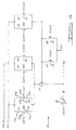
- Voltage buffer 32 supplies a bulk voltage to switch P1.
- Voltage buffer 32 is preferably configured as a source follower.
- Voltage buffer 32 is comprised of four PMOS transistors P8, P9, P10 and P11.
- PMOS transistor P8 has a drain terminal P8d, a bulk terminal P8b, a gate terminal P8g and a source terminal P8s.
- PMOS transistor P9 has a drain terminal P9d, a bulk terminal P9b, a gate terminal P9g and a source terminal P9s.
- PMOS transistor P10 has a drain terminal P10d, a bulk terminal P10b, a gate terminal P10g and a source terminal P10s.
- PMOS transistor P11 has a drain terminal P11d, a bulk terminal P11b, a gate terminal P11g and a source terminal P11s.
- Source terminal P8s is connected to bulk terminal P8b and both receive voltage VDD.
- Drain terminal P8d is connected to gate terminal P8g and both receive voltage VSS through a resistor R1 and gate terminal P9g.
- Source terminal P9s is connected to bulk terminal P9b and both receive voltage VDD.
- Drain terminal P9d is connected to source terminal P10s the junction of which forms the output voltage out1 of input buffer 32.
- Gate terminal P10g is connected to VSS.
- Bulk terminal P10b is connected to VDD.
- Drain terminal P10d is connected to source terminal P11s, the junction of which forms the output voltage out2 of input buffer 32.
- Bulk terminal P11b is directly connected to source terminal P11s. Drain terminal P10d is directly connected to VSS.
- voltages of the above circuit are dependent on the input 34 which is coupled to gate terminal P11g.
- voltage out2 is always greater than input 34 to insure the bulk-drain and bulk source junctions of switch P1 do not forward bias. Also, voltage out2 never falls below ground to insure the P-substrate-Nwell junction of P1 does not forward bias.
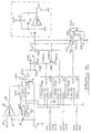
- Charge pump X9 has three parallel PMOS/NMOS combinations, each of which are identical with the exceptions noted below.
- Switches P4 and N4 have drain terminals P4d and N4d, bulk terminals P4b and N4b, gate terminals P4g and N4g and source terminals P4s and N4s, respectively.
- Drain terminal P4d is connected to source terminal N4s.
- Drain terminal N4d is connected to source terminal P4s.
- Gate terminal P4g is connected to inverted clock signal clk1.
- Bulk terminal P4b is connected to VDD.
- Gate terminal N4g is connected to clock signal clk 1.
- Bulk terminal N4b is connected to VSS.
- gate terminal P5g is connected to inverted clock signal clk3.
- Gate terminal N5g is connected to clock signal clk3.
- Gate terminal P6g is connected to inverted clock signal clk5.
- Gate terminal N6g is connected to clock signal clk5.
- Source terminal P4s and drain terminal N4d are connected to vref_low1.
- Source terminal P5s and drain terminal N5d are connected to vref_hi1.
- Source terminal P6s and drain terminal N6d are connected to vref_low1.
- the three NMOS/PMOS combinations are connected to two NMOS switches N7 and N8 and to a PMOS switch P7.
- Switches P7, N7 and N8 each have drain terminal P7d, N7d and N8d, bulk terminal P7b, N7b and N8b, gate terminal P7g, N7g and N8g and source terminal P7s, N7s and N8s, respectively.
- Source terminal N4s, drain terminal P4d, source terminal N5s and drain terminal P5d are connected to source terminal P7s and bulk terminal P7b.
- Source terminal N6s and drain terminal P6d are connected gate terminal P7g, drain terminal N7d and drain terminal N8d.
- Source terminal N7s and source terminal N8s are connected to VSS.
- Gate terminal N7g is connected to clock signal clk1.
- Gate terminal N8g is connected to clock signal clk3.
- Bulk terminals of N4 through N8 are connected to VSS.
- Clock signal clk2 is inverted in an inverter 40 and is capacitively coupled though a capacitor 42 which is connected to drain terminal P7d and output signal OUT9.
- Output signal OUT9 for charge pump X9 is connected to gate terminal P1g.
- Output signal OUT8 for charge pump X8 is connected to gate terminal P2g.
- Clock signals clk1 to clk 5 are shown as generated by clock generator 19.
- the groups of clock signals are preferably non-overlapping waveforms (i.e., they are not high simultaneously).
- the non-overlapping clock waveforms result in non-overlapping waveforms at P2g so that switch P1 and switch P2 are not conducting simultaneously.
- Vb1 is defined as input voltage Vin plus the absolute value of threshold voltage of P11 (FIG. 5). If Vb1 is less than the absolute value of threshold of P7, output signal OUT9 will be less than Vb1+Vbe.
- Vbe is the base-emitter voltage of a parasitic PNP transistor formed by the source terminal P7s (i.e., the emitter of the PNP), bulk terminal P4b (i.e., the base of the PNP) and the underlying substrate (i.e., the collector of the PNP).
- the on voltage does not follow Vin since the lower limit of Vb1 is VSS.
- the gate voltage of P1 thus has a lower limit of Vbe-Vdd.
- the gate-source voltage will eventually be too low to turn on switch P1.
- the absolute value of the threshold voltage of P11 is one volt and Vbe is one volt the gate-source "on"voltage is always between -2.5 volts and four volts for values of Vin from -1.5 volts to 5 volts and the gate-bulk voltage is around -5 volts.
- TDDB is minimised.
- Switch P1 turns off. During the high clock signal clk2, charge is transferred from capacitor C1 to capacitor C2. When clk2 goes low, a transition of zero to five volts is capacitively coupled to output signal OUT9.
- Charge pump X8 operates in a similar manner to charge X9. The only difference is that the input Vref_lo2 is connected to VSS since the drain of P2 is always connected to VSS. The on gate voltage of P2 is Vbe-VDD.
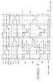
- FIGS. 6 through 8 the circuit of FIG. 1 has been modified for an embodiment where the maximum Vin exceeds five volts. (The previous example assumes a maximum Vin of five volts.) The following example presumes a maximum Vin of 6.5 volts. The reference numerals corresponding to components in FIG. 1 have been primed.
- Switch N20 has been added to drain terminal P2d' to block current flowing through P2' when Vin is greater than five volts.
- the output signal OUT8 of charge pump X8' has a maximum value of five volts.
- the switch P2' will conduct current.
- N20 becomes non-conducting to prevent P2' from conducting.
- Switch P2 prevents N20 from becoming forward biased when Vin is less than Vss.
- Switch P1 also should does not turn off when Vin is above five volts.
- PMOS switch P20 is used to turn off switch P1 when Vin is above five volts.
- Switch P20 is driven by charge pump X10 which is further described in connection with FIG. 8.
- Charge pump X10 is capable of generating voltages over five volts.
- switches N21 and P21 and a comparator 50 are provided.
- Switches P21 and N21 each have a drain terminal P21d and N21d, bulk terminal P21b and N21b, gate terminal P21g and N21g and a source terminal P21s and N21s.
- Comparator 50 has an inverting terminal 52, a non-inverting terminal 54 and an output terminal 56.
- Gate terminals P21g and N21g are connected to output terminal 56. Output voltage OUT2 from voltage buffer is connected to drain terminal N21d. Source terminals N21s and P21s and bulk terminal P21b are connected to bulk terminals P20b and P1b'. Drain terminal P21d is connected to source terminal P20s.
- Non-inverting terminal 54 is connected to voltage vag. Inverting terminal 52 is connected to input voltage Vin.
- Switch pair N21 and P21 operate to connect bulk terminals P20b and P1b' and P3b' to input voltage Vin through comparator 50 when Vin is greater than vag (i.e., P21 is on and N21 is off). When Vin is less than vag, comparator 50 turns off P21 and turns on N21 allowing voltage buffer 32' to drive bulk terminals P20b, P3' and P1b'. Both switches N21 and P21 are required to prevent undesirable forward biasing of either switch.
- Charge pump X10 has inputs Vref_hi3 and Vref_lo3 connected to outputs outl and out2 of voltage buffer 32', respectively. Output out10 of charge pump X10 is connected to gate terminal P20g and a collector PNP1c of transistor PNP1.
- Base terminal PNPlb is connected to base terminal P3b', P1b', P20b, P21b, P21s and N21s.
- Emitter terminal PNPle is connected to ground.
- charge pump X10 functions similarly to the charge pump of FIG. 4. However, the high portion of clock signal clk3 is divided into two signals clk3a and clk3b. Clock signal clk3a is another precharge phase. During clock clk3a, output OUT10 is driven toward the voltage of OUT1 of buffer 32. During clock phase clk3b, output OUT10 is driven toward the voltage of OUT1 of buffer 32 plus VDD.
- Charge pump X10 includes several MOSFET switches each having gate, source, bulk and drain terminals connected as shown.
- Drain terminal N22d is connected to input vref_lo3 of charge pump X10.
- Source terminal N22s is connected to drain terminal N23d.
- Drain terminal N24d is connected to input vref_hi3 of charge pump X10.
- Source terminal N24s is connected to drain terminal N23d and to drain terminal N25d.
- Source terminal N25s is connected to VSS.
- Gate terminal N22g is connected to clock signal clk1.
- Gate terminal N24g is connected to clock signal clk3a.
- Gate terminal N25g is connected to clock signal clk2.
- Bulk terminals N24b and N25b are connected to VSS.
- Gate terminal N23g is connected to Vdd.
- Source terminal N23s and bulk terminal P23b are connected to source terminals P22s and P23s and bulk terminal P22b.
- Gate terminal P23g is connected to inverted clock signal clk3b.
- Gate terminal P22g and drain terminal P23d are connected to drain terminal N26d.
- Gate terminal N26g is connected to VDD.
- Source terminal N26s is connected to drain terminals N27d, N28d, and N29d.
- Source terminals N27s, N28s, and N29s are connected to Vss.
- Gate terminals N27g, N28g, and N29g are connected to clock signals clk3a, clk1, and clk2, respectively.
- Drain terminal P22d is connected to output terminal OUT10.
- Source terminal P25s is connected to bulk terminal P25b and Vdd.
- Gate terminal P25g is connected to inverted clock signal clk3b. Drain terminal P25d is connected to one end of resistor 58.
- Source terminal N30s is connected to VSS.
- Gate terminal N30G is connected to clock signal clk2.
- Source terminal N31s is connected to VSS.
- Gate terminal N31g is connected to clock signal clk3a.
- Drain terminals N30d and N31d and one end of resistor 58 are connected to one electrode of capacitor 60. The opposite electrode of capacitor 60 is connected to output terminal OUT10.
- Switches N23 and N26 are used to protect N22, N24, N25, N27, N28 and N29 from excessive gate oxide voltages.
- the voltages at P23d and P23s may temporarily exceed 6.5 volts due to charge injection when the voltage at switch P23g transitions from zero to five volts.
- Switch N23 and N26 form a voltage divider so that the maximum gate oxide voltage across any switch is five volts.
- gate terminal P22g is shorted to source terminal P22s by switch P23. P22 is then off and the signal from output terminal OUT10 of charge pump X10 floats. At the same time, switch N25 causes a five volt transition in OUT 10 via capacitor 60. When the voltage of output signal OUT10 rises, the drain-to-bulk junction of P22 forward biases. The bulk voltage of P22 and P23 will track output signal OUT10. Transistor PNP1 clamps output signal OUT10 to Vb1+Vbe, which when Vin>vag, equates to output signal OUT10 to Vin+Vbe. This turns P20 off when Vin is 6.5 volts. Thus, the maximum gate voltage of P20 when driven by charge pump X10 is Vin+Vbe which is higher than charge pump X9 would provide. Thus, when Vin exceeds the power supply voltage, charge pump X10 is used to control P1.
Landscapes
- Physics & Mathematics (AREA)
- General Physics & Mathematics (AREA)
- Electronic Switches (AREA)
- Logic Circuits (AREA)
- Dc-Dc Converters (AREA)
- Filters That Use Time-Delay Elements (AREA)
- Manipulation Of Pulses (AREA)
Description
Claims (11)
- An interface circuit interfacing a sensor (12) to a switched capacitor circuit (20) and a processing component (14), said processing component (14) having a power supply voltage range, said sensor having a sensor output in a voltage range outside said power supply voltage range, said interface circuit comprising:
a MOSFET (P1) coupled between said sensor and said switched capacitor circuit (20) for connecting said sensor output to said switched capacitor circuit, said MOSFET having a gate oxide layer (31), a switch conducting-state resistance, a gate voltage and a bulk voltage;
characterised in that there is provided;
a control circuit (22) coupled to said sensor output and to said MOSFET (P1), said control circuit (22) continually adjusting said gate voltage and said bulk voltage in relation to the voltage of said sensor output to prevent a voltage across said gate oxide layer (31) from exceeding a predetermined value. - An interface circuit as claimed in claim 1, wherein said predetermined value corresponds to time dependent dielectric breakdown.
- An interface circuit as claimed in claim 1 or 2, wherein said control circuit maintains a predetermined conducting state resistance for said MOSFET switch.
- An interface circuit as claimed in any one of claims 1 to 3, wherein said MOSFET switch comprises a PMOS switch.
- An interface circuit as claimed in any one of the preceding claims comprising;a second MOSFET switch (P2) connected to the first said MOSFET switch (P1), said second MOSFET switch (P2) having a bulk-source junction and a conducting state;the control circuit (22) comprising;a voltage buffer (32) connected to said first MOSFET switch (P1), said voltage buffer (32) having a voltage buffer output voltage greater than the voltage of said sensor output;a first charge pump (X9) connected to said first MOSFET switch (P1) generating a first control voltage, said first charge pump (X9) selectively and continually adjusting said first control voltage in relation to the voltage of said sensor output to prevent time dependent dielectric breakdown of said gate oxide layer;and a second charge pump (X8) connected to said second MOSFET switch (P2), said second charge pump (X8) generating a second control voltage, said second charge pump (X8) adjusting said second control voltage so that when said second MOSFET switch (P2) is conducting said bulk-source junction of said second MOSFET switch (P2) is forward biased;and the switched capacitor circuit (20) being electrically coupled to said first MOSFET switch (P1) and said second MOSFET switch (P2) so as to provide a translated output corresponding to a predetermined translation of said sensor output to within said power supply voltage range of said processing component (14).
- An interface circuit as claimed in claim 5 further comprising a third MOSFET switch (N20) coupled to said second MOSFET switch (P2') for preventing said second MOSFET switch (P2') from conducting current when the voltage of said sensor output is greater than said power supply voltage.
- An interface circuit as claimed in claim 5 or 6, wherein said voltage buffer (32) includes a source follower circuit.
- An interface circuit as claimed in claim 6 further comprising a third charge pump (X10'), a PNP transistor, and a fourth MOSFET switch (P20) operatively connected to said first MOSFET switch (P1'), said third charge pump (X10'), said PNP transistor and said fourth MOSFET switch (P20) controlling said first MOSFET switch (P1') when said sensor output voltage exceeds said power supply voltage.
- An interface circuit as claimed in claim 6 further comprising a fourth MOSFET switch means (N21,P21), a comparator circuit (50), and a reference voltage (VAG), said comparator having an output terminal, an inverting input terminal, and a non-inverting input terminal, said comparator output terminal connected to said fourth MOSFET switch means (N21,P21), said inverting input terminal connected to said sensor output and said non-inverting input terminal connected to said reference voltage (VAG) said fourth MOSFET switch means coupling said comparator output terminal to said first MOSFET switch means when said sensor output voltage is greater than said reference voltage.
- An interface circuit as claimed in claim 9, wherein said reference voltage (VAG) is half of said power supply voltage.
- An interface circuit as claimed in claim 9, wherein said switched capacitor circuit (20) comprises;an operational amplifier (24) having an output terminal (30), an inverting input terminal (26), and a non-inverting input terminal (28),a first capacitor (C2) selectively switched between said inverting input terminal (26) and said output terminal (30) anda second capacitor (C1) connected to said inverting input terminal (26) of said operational amplifier (24),the reference voltage (VAG) being connected to said non-inverting terminal (28), andsaid second capacitor (C1) capacitively coupling said switched capacitor circuit (20) to said first MOSFET switch (P1).
Applications Claiming Priority (2)
| Application Number | Priority Date | Filing Date | Title |
|---|---|---|---|
| US432378 | 1995-05-01 | ||
| US08/432,378 US5541531A (en) | 1995-05-01 | 1995-05-01 | Switch capacitor interface circuit |
Publications (3)
| Publication Number | Publication Date |
|---|---|
| EP0741350A2 EP0741350A2 (en) | 1996-11-06 |
| EP0741350A3 EP0741350A3 (en) | 1998-11-18 |
| EP0741350B1 true EP0741350B1 (en) | 2001-10-17 |
Family
ID=23715902
Family Applications (1)
| Application Number | Title | Priority Date | Filing Date |
|---|---|---|---|
| EP96303060A Expired - Lifetime EP0741350B1 (en) | 1995-05-01 | 1996-05-01 | Switch capacitor interface circuit |
Country Status (4)
| Country | Link |
|---|---|
| US (1) | US5541531A (en) |
| EP (1) | EP0741350B1 (en) |
| JP (1) | JPH08307212A (en) |
| DE (1) | DE69615910T2 (en) |
Cited By (1)
| Publication number | Priority date | Publication date | Assignee | Title |
|---|---|---|---|---|
| CN101488755B (en) * | 2008-01-14 | 2010-12-29 | 盛群半导体股份有限公司 | CMOS series comparator, single terminal CMOS phase reverser and control method therefor |
Families Citing this family (9)
| Publication number | Priority date | Publication date | Assignee | Title |
|---|---|---|---|---|
| SE510612C2 (en) | 1996-11-08 | 1999-06-07 | Ericsson Telefon Ab L M | Method and apparatus for direct current matching a first circuit to at least a second circuit |
| US5959853A (en) * | 1998-08-24 | 1999-09-28 | Kos; Marek John | Closed-loop switched capacitor network power supply |
| ITTO20020263A1 (en) * | 2002-03-25 | 2003-09-25 | Sila Holding Ind Spa | INTERFACE CIRCUIT BETWEEN A CONTINUOUS VOLTAGE SOURCE AND A LOAD PILOTING CIRCUIT, PARTICULARLY FOR ON BOARD USE |
| US6828851B1 (en) * | 2002-10-31 | 2004-12-07 | National Semiconductor Corporation | Constant voltage charge-pump circuit with feedback |
| DE10357785B3 (en) * | 2003-12-10 | 2005-05-04 | Infineon Technologies Ag | Linear switched capacitor circuit device using integrated deep-sub-micron technology has thick oxide transistors used in switched capacitor circuit |
| CN100516893C (en) * | 2007-07-04 | 2009-07-22 | 深圳市长运通集成电路设计有限公司 | Programmable voltage monitoring circuit |
| CN103872900A (en) * | 2012-12-11 | 2014-06-18 | 中芯国际集成电路制造(上海)有限公司 | Method for improving efficiency of charge pump |
| US9048777B2 (en) * | 2012-12-31 | 2015-06-02 | Silicon Laboratories Inc. | Apparatus for integrated circuit interface and associated methods |
| US10215589B2 (en) * | 2015-08-12 | 2019-02-26 | Infineon Technologies Ag | IO matching current modulated output for sensors |
Family Cites Families (13)
| Publication number | Priority date | Publication date | Assignee | Title |
|---|---|---|---|---|
| US4438473A (en) * | 1981-07-21 | 1984-03-20 | The United States Of America As Represented By The Secretary Of The Interior | Power supply for an intrinsically safe circuit |
| US4405964A (en) * | 1982-03-29 | 1983-09-20 | Zenith Radio Corporation | Over voltage circuit for a switching regulator power supply |
| US4493092A (en) * | 1982-12-17 | 1985-01-08 | Gte Automatic Electric, Inc. | Interface circuit for digital signal transmission system |
| EP0220816B1 (en) * | 1985-10-23 | 1992-06-10 | Pilkington Micro-Electronics Limited | Gated transmission circuit (on-chip) |
| US4710647A (en) * | 1986-02-18 | 1987-12-01 | Intel Corporation | Substrate bias generator including multivibrator having frequency independent of supply voltage |
| US4716319A (en) * | 1986-08-04 | 1987-12-29 | Motorola, Inc. | Switched capacitor filter for low voltage applications |
| US4752699A (en) * | 1986-12-19 | 1988-06-21 | International Business Machines Corp. | On chip multiple voltage generation using a charge pump and plural feedback sense circuits |
| JPH0695545B2 (en) * | 1988-01-07 | 1994-11-24 | 株式会社東芝 | Semiconductor integrated circuit |
| US5003197A (en) * | 1989-01-19 | 1991-03-26 | Xicor, Inc. | Substrate bias voltage generating and regulating apparatus |
| US5057707A (en) * | 1989-07-05 | 1991-10-15 | Motorola, Inc. | Charge pump including feedback circuitry for eliminating the requirement of a separate oscillator |
| DE3940537A1 (en) * | 1989-12-07 | 1991-06-13 | Endress Hauser Gmbh Co | ARRANGEMENT FOR PROCESSING SENSOR SIGNALS |
| US5140196A (en) * | 1991-04-15 | 1992-08-18 | Motorola, Inc. | Variable level translator |
| JP3337241B2 (en) * | 1991-07-26 | 2002-10-21 | テキサス インスツルメンツ インコーポレイテツド | Improved multi-channel sensor interface circuit and manufacturing method thereof |
-
1995
- 1995-05-01 US US08/432,378 patent/US5541531A/en not_active Expired - Fee Related
-
1996
- 1996-04-24 JP JP8102843A patent/JPH08307212A/en active Pending
- 1996-05-01 DE DE69615910T patent/DE69615910T2/en not_active Expired - Fee Related
- 1996-05-01 EP EP96303060A patent/EP0741350B1/en not_active Expired - Lifetime
Cited By (1)
| Publication number | Priority date | Publication date | Assignee | Title |
|---|---|---|---|---|
| CN101488755B (en) * | 2008-01-14 | 2010-12-29 | 盛群半导体股份有限公司 | CMOS series comparator, single terminal CMOS phase reverser and control method therefor |
Also Published As
| Publication number | Publication date |
|---|---|
| EP0741350A3 (en) | 1998-11-18 |
| US5541531A (en) | 1996-07-30 |
| JPH08307212A (en) | 1996-11-22 |
| DE69615910D1 (en) | 2001-11-22 |
| EP0741350A2 (en) | 1996-11-06 |
| DE69615910T2 (en) | 2002-05-29 |
Similar Documents
| Publication | Publication Date | Title |
|---|---|---|
| US7282894B2 (en) | Method and apparatus for performing lossless sensing and negative inductor currents in a high side switch | |
| US6445244B1 (en) | Current measuring methods | |
| US7176742B2 (en) | Bootstrapped switch with an input dynamic range greater than supply voltage | |
| US6525574B1 (en) | Gate bootstrapped CMOS sample-and-hold circuit | |
| EP0969344A2 (en) | Semiconductor integrated circuit including voltage follower circuit | |
| EP0741350B1 (en) | Switch capacitor interface circuit | |
| CN109213248B (en) | Negative power supply control circuit and power supply device | |
| JP2916505B2 (en) | Comparison circuit | |
| US6429696B1 (en) | Peak hold and calibration circuit | |
| US6466076B2 (en) | Variable delay circuit having a ramp voltage generating unit | |
| US5148054A (en) | High accuracy MOSFET-switched sampling circuit | |
| US20020030535A1 (en) | Dynamic bias circuitry utilizing early voltage clamp and translinear techniques | |
| JP2975378B2 (en) | Track and hold circuit | |
| US20210391838A1 (en) | Switched-capacitor amplifier | |
| JPS62258521A (en) | Analog-digital converter | |
| US6693479B1 (en) | Boost structures for switched-capacitor systems | |
| US5625304A (en) | Voltage comparator requiring no compensating offset voltage | |
| US11611341B2 (en) | Sampling circuit and sampling method | |
| US8232904B2 (en) | Folding analog-to-digital converter | |
| US20090039924A1 (en) | Systems and methods for reducing distortion in semiconductor based sampling systems | |
| US20190199337A1 (en) | Comparator | |
| US20220021380A1 (en) | Analog Switch with Boost Current for Fast Turn On | |
| US20040189356A1 (en) | Power-on detector, and power-on reset circuit using the same | |
| US6480065B1 (en) | CMOS folding amplifier having high resolution and low power consumption | |
| US10892617B2 (en) | High speed wide dynamic range input structure |
Legal Events
| Date | Code | Title | Description |
|---|---|---|---|
| PUAI | Public reference made under article 153(3) epc to a published international application that has entered the european phase |
Free format text: ORIGINAL CODE: 0009012 |
|
| AK | Designated contracting states |
Kind code of ref document: A2 Designated state(s): DE FR GB |
|
| PUAL | Search report despatched |
Free format text: ORIGINAL CODE: 0009013 |
|
| AK | Designated contracting states |
Kind code of ref document: A3 Designated state(s): DE FR GB |
|
| 17P | Request for examination filed |
Effective date: 19981127 |
|
| 17Q | First examination report despatched |
Effective date: 20000208 |
|
| GRAG | Despatch of communication of intention to grant |
Free format text: ORIGINAL CODE: EPIDOS AGRA |
|
| GRAG | Despatch of communication of intention to grant |
Free format text: ORIGINAL CODE: EPIDOS AGRA |
|
| GRAH | Despatch of communication of intention to grant a patent |
Free format text: ORIGINAL CODE: EPIDOS IGRA |
|
| GRAH | Despatch of communication of intention to grant a patent |
Free format text: ORIGINAL CODE: EPIDOS IGRA |
|
| GRAA | (expected) grant |
Free format text: ORIGINAL CODE: 0009210 |
|
| AK | Designated contracting states |
Kind code of ref document: B1 Designated state(s): DE FR GB |
|
| PG25 | Lapsed in a contracting state [announced via postgrant information from national office to epo] |
Ref country code: FR Free format text: LAPSE BECAUSE OF FAILURE TO SUBMIT A TRANSLATION OF THE DESCRIPTION OR TO PAY THE FEE WITHIN THE PRESCRIBED TIME-LIMIT Effective date: 20011017 |
|
| REF | Corresponds to: |
Ref document number: 69615910 Country of ref document: DE Date of ref document: 20011122 |
|
| REG | Reference to a national code |
Ref country code: GB Ref legal event code: IF02 |
|
| PG25 | Lapsed in a contracting state [announced via postgrant information from national office to epo] |
Ref country code: GB Free format text: LAPSE BECAUSE OF NON-PAYMENT OF DUE FEES Effective date: 20020501 |
|
| EN | Fr: translation not filed | ||
| PLBE | No opposition filed within time limit |
Free format text: ORIGINAL CODE: 0009261 |
|
| STAA | Information on the status of an ep patent application or granted ep patent |
Free format text: STATUS: NO OPPOSITION FILED WITHIN TIME LIMIT |
|
| 26N | No opposition filed | ||
| PG25 | Lapsed in a contracting state [announced via postgrant information from national office to epo] |
Ref country code: DE Free format text: LAPSE BECAUSE OF NON-PAYMENT OF DUE FEES Effective date: 20021203 |
|
| GBPC | Gb: european patent ceased through non-payment of renewal fee |
Effective date: 20020501 |