EP0740427A1 - Transmitting and receiving apparatus - Google Patents
Transmitting and receiving apparatus Download PDFInfo
- Publication number
- EP0740427A1 EP0740427A1 EP96106638A EP96106638A EP0740427A1 EP 0740427 A1 EP0740427 A1 EP 0740427A1 EP 96106638 A EP96106638 A EP 96106638A EP 96106638 A EP96106638 A EP 96106638A EP 0740427 A1 EP0740427 A1 EP 0740427A1
- Authority
- EP
- European Patent Office
- Prior art keywords
- transmitting
- changeover switch
- circulator
- diodes
- power
- Prior art date
- Legal status (The legal status is an assumption and is not a legal conclusion. Google has not performed a legal analysis and makes no representation as to the accuracy of the status listed.)
- Granted
Links
Images


Classifications
-
- H—ELECTRICITY
- H04—ELECTRIC COMMUNICATION TECHNIQUE
- H04B—TRANSMISSION
- H04B1/00—Details of transmission systems, not covered by a single one of groups H04B3/00 - H04B13/00; Details of transmission systems not characterised by the medium used for transmission
- H04B1/38—Transceivers, i.e. devices in which transmitter and receiver form a structural unit and in which at least one part is used for functions of transmitting and receiving
- H04B1/40—Circuits
- H04B1/44—Transmit/receive switching
- H04B1/48—Transmit/receive switching in circuits for connecting transmitter and receiver to a common transmission path, e.g. by energy of transmitter
-
- H—ELECTRICITY
- H04—ELECTRIC COMMUNICATION TECHNIQUE
- H04B—TRANSMISSION
- H04B1/00—Details of transmission systems, not covered by a single one of groups H04B3/00 - H04B13/00; Details of transmission systems not characterised by the medium used for transmission
- H04B1/38—Transceivers, i.e. devices in which transmitter and receiver form a structural unit and in which at least one part is used for functions of transmitting and receiving
- H04B1/40—Circuits
- H04B1/44—Transmit/receive switching
Definitions
- the present invention relates to a transmitting and receiving apparatus wherein an antenna is shared by a transmission system and a receiving system, and more particularly to an automatic switching arrangement for interconnecting the transmission system, the receiving system, and the antenna.
- a transmitting and receiving apparatus In the field of mobile communications, a transmitting and receiving apparatus is used in which a single antenna is shared by its transmitting and receiving systems. In this type of apparatus, a switching or duplexing method is employed for separating the transmitting and receiving systems to avoid mixing the transmitted and received signals.
- Fig. 7 is a schematic diagram of a conventional transmitting and receiving apparatus including digital communication equipment using the time division multiple access (TDMA) and time division duplex (TDD) systems.
- TDMA time division multiple access
- TDD time division duplex
- a changeover switch 22 is disposed in the feed line to a single antenna 21, and is connected to a transmitter 23 and a receiver 24, whereby the antenna 21 can be connected to either the transmitter 23 or the receiver 24 through the switch 22.
- an isolator 25 is connected between the switch 22 and the transmitter 23 for preventing the generation of intermodulation (IM) due to reflection of a transmitted signal as well as for avoiding unstable operation of a power amplifier (PA) caused by load fluctuations.
- IM intermodulation
- PA power amplifier
- Fig. 8 is a circuit diagram of the changeover switch 22.
- the switch 22 includes coupling capacitors C1 to C3 and a high-frequency short-circuiting capacitor C4.
- a 1/4-wavelength high-impedance line L1 is short-circuited at one end by the capacitor C4 at high frequencies, thus making the impedance of the input terminal of switching power viewed from the other end P1 infinite and resulting in the input terminal being in an open state at high frequencies.
- the switch 22 also has diodes D1 and D2 and a 1/4-wavelength stripline L2 having characteristic impedance Z0 which is equal to a circuit impedance, generally 50 ⁇ .
- the switching current is discontinued to turn off the diodes D1 and D2. Accordingly, the points P1 and P2 are disconnected from each other by the diode D1, and the point P3 is disconnected from ground by the diode D2. Thus, a received signal input through the antenna 21 can be completely conducted to the receiving circuit.
- the transmitting and receiving apparatus of the above conventional type requires a battery for providing a switching current in order to switch between the transmitting and receiving operations and also requires a current control circuit. This deteriorates the power efficiency of the transmitting and receiving apparatus and also shortens battery life. Further, the provision of a current control circuit inevitably enlarges the overall apparatus and increases its cost. There is also a problem of low reliability in the performance of the apparatus, for example, since any erroneous operation of the current control circuit renders the apparatus inoperable.
- a measure that has been considered but has not yet been published or patented, to overcome the above-described drawbacks inherent in the conventional apparatuses, may be the use of a changeover switch 30 as illustrated in Fig. 9 for automatically switching between the transmitting and receiving systems depending on an output voltage of a transmitting signal.
- the switch 30 includes diodes D3 to D6 and a 1/4-wavelength stripline L3 having characteristic impedance Z0. This switch 30 takes advantage of the fact that the transmitting power is greater than the receiving power. For example, in the Personal Handyphone System (PHS), the peak receiving power is several dozens of ⁇ W, while the transmitting power is approximately 100 mW.
- PHS Personal Handyphone System
- a high-frequency signal having approximately 100 mW of power is outputted.
- diodes D3 to D6 one of the diodes D3 and D4 or one of the diodes D5 and D6 is accordingly turned on when the transmitted signal exceeds 10 mW.
- Which diodes are on, from among diodes D3 or D4, and D5 or D6, depends on the polarity of the voltage: a positive voltage turns on the diodes D3 and D5, while a negative voltage turns on the diodes D4 and D6.
- a branch point P4 and the terminal of the transmitting circuit are electrically connected through the diodes D3 and D4 at high-frequencies.
- a point P5 is short-circuited to ground through the diodes D5 and D6 so that the impedance of a portion viewed from the point P4 to the receiving circuit can be infinite, thus resulting in this portion being in an open state.
- a transmitted signal is mostly radiated from the antenna, and partially reflected by the antenna and absorbed in the isolator before returning to the transmitting circuit.
- the configuration of the changeover switch 30 makes it possible to eliminate the need for the provision of a battery and a current control circuit for providing a switching current. This improves the power efficiency of the transmitting and receiving apparatus, thereby avoiding an increase in the size and cost of the apparatus, as well as enhancing the reliability of its performance.
- Diodes have different signal passing characteristics depending on input power; in general, a larger amount of power passing through a diode decreases its insertion loss (I. L.).
- I. L. insertion loss
- the I. L. is substantially constant regardless of the power of a transmitted signal.
- the I. L. is susceptible to varying, and more specifically, a smaller amount of power increases the I. L., thereby causing a degradation in the performance of the overall apparatus.
- a signal passes through the switch during a transmitting operation, which increases losses in the transmission system and further degrades the power efficiency.
- a switch having high isolation characteristics is also required for switching between the transmitting and receiving systems, thereby increasing the cost of parts.
- a transmitting and receiving apparatus including a transmitter and a receiver that share a single antenna, comprising: a circulator disposed for interconnecting the transmitter, the receiver, and the antenna; a terminating resistor provided between ground and a point where the circulator and the receiver are connected; and a changeover switch disposed between the terminating resistor and the above point of connection so that it automatically connects the circulator to the terminating resistor in response to input power supplied from the transmitter during transmission.
- Another aspect of the invention relates to a changeover switch for use in the above transmitting and receiving apparatus.
- a circulator is disposed at the branch portion of the antenna, and also, a changeover switch is provided between the terminating resistor and a point where the circulator and the receiver are connected so that it can be automatically switched to connect the circulator to the terminating resistor in response to transmission power.
- the apparatus is free from fluctuations in the I. L. caused by changes in the power of a transmitted signal, thereby avoiding deterioration in performance.
- the transmitted signal does not pass through the switch, which eliminates the need for the use of a switch that has low insertion losses, thereby decreasing the cost of parts.
- the transmitted signal and the received signal are separated by the circulator, it is not necessary to use a switch having high isolation characteristics which is conventionally required. This also contributes to a reduction in the cost of parts.
- the circulator whose port is terminated during transmission serves as an isolator, thereby precluding IM generation by the transmission system and also ensuring stable PA operation without being influenced by load fluctuations.
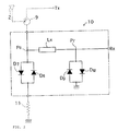
- Figs. 1 and 2 illustrate a transmitting and receiving apparatus according to an embodiment of the present invention. More specifically, Fig. 1 is a schematic diagram of the transmitting and receiving apparatus; and Fig. 2 is a circuit diagram of a changeover switch for use in the apparatus according to this embodiment.
- a single antenna 2 is shared by a transmitter 3 and a receiver 4 via a circulator 9 disposed at the feed point A of the antenna 2.
- a PA 6 for amplifying transmitted signals is disposed between the transmitter 3 and the feed point A, and a low-noise amplifier (LNA) 7 and a band-pass filter 8 are connected between the receiver 4 and the feed point A.
- the circulator 9 located at the feed point A serves the function of allowing signals to pass only in the transmitting direction and preventing them from flowing in the reverse direction.
- a changeover switch 10 intervenes between the circulator 9 and the LNA 7 of the receiver 4, and a terminating resistor 11 is located between one terminal of the switch 10 and ground.
- the above-described changeover switch 10 is configured as shown in Fig. 2.
- Diodes D7 and D8 are connected in parallel to each other between the circulator 9 and the terminating resistor 11.
- a 1/4-wavelength stripline L4 having characteristic impedance Z0 is connected to a point P6 located between the diodes D7 and D8.
- Diodes D9 and D10 are connected in parallel to each other between the other end of the stripline L4 and ground.
- the receiver (Rx system) is connected to a point P7 positioned between the diodes D9 and D10.
- the changeover switch 10 will now be explained by its application to a PHS system by way of example.
- a high-frequency signal of approximately 100 mW is outputted from the transmitter 3.
- a high-frequency signal of approximately several dozens of mW flows through the switch 10 via the circulator 9 after the signal has been partially reflected by the antenna 2.
- diodes that are turned on at 10 mW as the diodes D7 to D10, it is arranged that one of the diodes D7 and D8 and one of the diodes D9 and D10 are turned on if the high-frequency signal exceeds 10 mW.
- a positive voltage turns on the diodes D7 and D9, while a negative voltage turns on the diodes D8 and D10.
- the point P7 is short-circuited to the ground through either diode D9 or diode D10, the impedance of a portion viewed from the point P6 toward the receiver 4 becomes infinite, thus resulting in this portion being in an open state.
- the point P6 is connected to the terminating resistor 11 through either diode D7 or diode D8, whereby 10 mW or more signal power is absorbed and dissipated in the resistor 11.
- no diodes are provided for the transmitter 3, which would otherwise produce adverse influences on the apparatus caused by the non-linearity of diodes. This further precludes losses caused by diodes and suppresses fluctuations in the I. L. caused by changes in transmission power.
- Fig. 3 is a circuit diagram of an alternate embodiment of a changeover switch and Fig. 4 illustrates a micro-stripline, both of these components being used in an experiment carried out for ensuring the advantages of this embodiment.
- the changeover switch shown in Fig. 3 for use in a 950 MHz frequency band was produced by the use of various types of commercially-available devices, as shown in Table 1.
- Table 1 Device List Device Manufacturer Item of product Diode NEC Corporation ISS283 Resistor Rohm Co.,Ltd. MCR03 Micro-stripline Mitsubishi Gas Chemical Co.,Inc. CCK-HL870
- Table 2 shows the measurements of electrical characteristics, such as reflection losses (dB) and insertion losses (I. L.) (dB), caused as a result of varying incident power at 950 MHz from 100 ⁇ W to 100 mW.
- the reflection losses indicate reflection characteristics viewed from a point P8 of Fig. 3, and the I. L. designate losses resulting in a portion from point 8 to point 9 of Fig. 3.
- Figs. 5A and 5B are characteristic diagrams indicating reflection losses with respect to the incident power 100 ⁇ W and 100 mW, respectively.
- Figs. 6A and 6B are characteristic diagrams designating the I. L. with respect to the incident power 100 ⁇ W and 100 mW, respectively.
- the reflection losses with respect to various frequencies are 18dB or greater in response to a change of the incident power from 100 ⁇ W and 100 mW when the receiving power is 100 ⁇ W and the transmission power is 100 mW. This indicates that a signal reflected from the antenna is too weak to flow into the transmitter, thereby preventing IM generation and unstable PA operations.
- a received signal passes through the switch with the I. L. of 0.9 dB and further passes through the LNA and BPF, followed by finally flowing into the receiver. Since the received signal is amplified in the LNA, the above-mentioned I. L. do not present any substantial problem.
- the circulator 9 is disposed at the feed point A of the antenna 2, and also, the changeover switch 10 is provided between the circulator 9 and the receiver 4 to perform an automatic switching operation in accordance with transmission power.
- This obviates the need for the provision of a battery for switching a current and a current control circuit, as has been conventionally required, thereby improving the power efficiency of the overall transmitting and receiving apparatus and also enhancing the reliability in its performance, as well as avoiding an increase in the size and costs of the apparatus.
- the apparatus is free from fluctuations in the I. L. caused by a change in power of a transmitted signal, which further avoids deterioration in performance.
- the transmitted signal does not pass through the switch 10, which eliminates the need for a switch especially designed to suppress insertion losses to a low level, thereby decreasing the cost of parts.
- the transmitted signal and the received signal are separated by the circulator 9, it is not necessary to use a switch having high isolation characteristics, as has been conventionally required. This also contributes to a reduction in the cost of parts, thereby meeting a demand for lower prices of the apparatus.
- the circulator 9 serves as an isolator during transmission, thereby precluding IM generation in the transmission system and ensuring stable PA operations without being influenced by load fluctuations.
- the transmitting and receiving apparatus of the present invention offers the following advantages.
- a circulator is provided at the feed point of the antenna, and a changeover switch is disposed between the terminating resistor and the point of connection between the circulator and the receiver so that it can be automatically switched to the resistor in response to power inputted from the transmitter during transmission.
- fluctuations in the I. L. caused by a change in transmission power can be prevented without requiring the provision of a battery and a current control circuit for providing a switching current. It is also possible to suppress losses of the transmission system and improve the power efficiency, as well as to decrease the cost of parts.
Landscapes
- Engineering & Computer Science (AREA)
- Computer Networks & Wireless Communication (AREA)
- Signal Processing (AREA)
- Transceivers (AREA)
- Control Of Motors That Do Not Use Commutators (AREA)
- Transmitters (AREA)
Abstract
Description
- The present invention relates to a transmitting and receiving apparatus wherein an antenna is shared by a transmission system and a receiving system, and more particularly to an automatic switching arrangement for interconnecting the transmission system, the receiving system, and the antenna.
- In the field of mobile communications, a transmitting and receiving apparatus is used in which a single antenna is shared by its transmitting and receiving systems. In this type of apparatus, a switching or duplexing method is employed for separating the transmitting and receiving systems to avoid mixing the transmitted and received signals.
- Fig. 7 is a schematic diagram of a conventional transmitting and receiving apparatus including digital communication equipment using the time division multiple access (TDMA) and time division duplex (TDD) systems. In this transmitting and receiving apparatus generally indicated by 20, a
changeover switch 22 is disposed in the feed line to asingle antenna 21, and is connected to atransmitter 23 and areceiver 24, whereby theantenna 21 can be connected to either thetransmitter 23 or thereceiver 24 through theswitch 22. Also, anisolator 25 is connected between theswitch 22 and thetransmitter 23 for preventing the generation of intermodulation (IM) due to reflection of a transmitted signal as well as for avoiding unstable operation of a power amplifier (PA) caused by load fluctuations. - Fig. 8 is a circuit diagram of the
changeover switch 22. Theswitch 22 includes coupling capacitors C1 to C3 and a high-frequency short-circuiting capacitor C4. A 1/4-wavelength high-impedance line L1 is short-circuited at one end by the capacitor C4 at high frequencies, thus making the impedance of the input terminal of switching power viewed from the other end P1 infinite and resulting in the input terminal being in an open state at high frequencies. Theswitch 22 also has diodes D1 and D2 and a 1/4-wavelength stripline L2 having characteristic impedance Z0 which is equal to a circuit impedance, generally 50 Ω. - An explanation will now be given of the transmitting and receiving operation of the
changeover switch 22. In the transmitting operation, a switching current is allowed to flow through theswitch 22 so as to turn on the diodes D1 and D2. This causes a point P3 to be short-circuited to ground through the diode D2, whereby a portion of the circuit viewed from a point P2 at one end of the stripline L2 toward the receiving circuit has an infinite impedance and is in an open state at high frequencies. On the other hand, since the points P1 and P2 are short-circuited to each other through the diode D1, a transmitted signal from the transmitting circuit is radiated from theantenna 21. This transmitted signal is partially absorbed in theisolator 25, thereby preventing the IM generation and unstable PA operations. - In a receiving operation, the switching current is discontinued to turn off the diodes D1 and D2. Accordingly, the points P1 and P2 are disconnected from each other by the diode D1, and the point P3 is disconnected from ground by the diode D2. Thus, a received signal input through the
antenna 21 can be completely conducted to the receiving circuit. - However, the transmitting and receiving apparatus of the above conventional type requires a battery for providing a switching current in order to switch between the transmitting and receiving operations and also requires a current control circuit. This deteriorates the power efficiency of the transmitting and receiving apparatus and also shortens battery life. Further, the provision of a current control circuit inevitably enlarges the overall apparatus and increases its cost. There is also a problem of low reliability in the performance of the apparatus, for example, since any erroneous operation of the current control circuit renders the apparatus inoperable.
- A measure that has been considered but has not yet been published or patented, to overcome the above-described drawbacks inherent in the conventional apparatuses, may be the use of a
changeover switch 30 as illustrated in Fig. 9 for automatically switching between the transmitting and receiving systems depending on an output voltage of a transmitting signal. Theswitch 30 includes diodes D3 to D6 and a 1/4-wavelength stripline L3 having characteristic impedance Z0. Thisswitch 30 takes advantage of the fact that the transmitting power is greater than the receiving power. For example, in the Personal Handyphone System (PHS), the peak receiving power is several dozens of µW, while the transmitting power is approximately 100 mW. - The transmitting and receiving operation of the switch circuit of Fig. 9 will now be explained in connection with its application to the PHS system by way of example.
- During a transmitting operation, a high-frequency signal having approximately 100 mW of power is outputted. By the use of diodes that are turned on by 10 mW of power, as the diodes D3 to D6, one of the diodes D3 and D4 or one of the diodes D5 and D6 is accordingly turned on when the transmitted signal exceeds 10 mW. Which diodes are on, from among diodes D3 or D4, and D5 or D6, depends on the polarity of the voltage: a positive voltage turns on the diodes D3 and D5, while a negative voltage turns on the diodes D4 and D6. At this time, a branch point P4 and the terminal of the transmitting circuit are electrically connected through the diodes D3 and D4 at high-frequencies. A point P5 is short-circuited to ground through the diodes D5 and D6 so that the impedance of a portion viewed from the point P4 to the receiving circuit can be infinite, thus resulting in this portion being in an open state. Hence, a transmitted signal is mostly radiated from the antenna, and partially reflected by the antenna and absorbed in the isolator before returning to the transmitting circuit.
- On the other hand, during a receiving operation, all the diodes D3 to D6 are turned off, since the receiving power inputted from the antenna is only several dozens of µW. Thus the point P4 is disconnected from the terminal of the transmitting circuit by the diodes D3 and D4 and also the point P5 is disconnected from ground by the diodes D5 and D6. Accordingly, a received signal inputted from the antenna can be completely sent to the receiving circuit.
- In this manner, the configuration of the
changeover switch 30 makes it possible to eliminate the need for the provision of a battery and a current control circuit for providing a switching current. This improves the power efficiency of the transmitting and receiving apparatus, thereby avoiding an increase in the size and cost of the apparatus, as well as enhancing the reliability of its performance. - Diodes have different signal passing characteristics depending on input power; in general, a larger amount of power passing through a diode decreases its insertion loss (I. L.). In the foregoing
conventional changeover switch 22, however, since a large amount of power is supplied from a battery, the I. L. is substantially constant regardless of the power of a transmitted signal. However, if automatic switching is performed according to the power of the transmitted signal, as in thechangeover switch 30, the I. L. is susceptible to varying, and more specifically, a smaller amount of power increases the I. L., thereby causing a degradation in the performance of the overall apparatus. - Moreover, whichever
switch - Accordingly, in view of the above background, it is an object of the present invention to provide a transmitting and receiving apparatus which does not have fluctuations in insertion losses caused by changes in transmission power, which does not require the provision of a battery and a current control circuit for providing a switching current so as to improve its reliability, which has reduced losses in its transmission system so as to enhance its power efficiency, and which has lower-cost parts.
- In order to achieve the above objects, according to an aspect of the present invention, there is provided a transmitting and receiving apparatus including a transmitter and a receiver that share a single antenna, comprising: a circulator disposed for interconnecting the transmitter, the receiver, and the antenna; a terminating resistor provided between ground and a point where the circulator and the receiver are connected; and a changeover switch disposed between the terminating resistor and the above point of connection so that it automatically connects the circulator to the terminating resistor in response to input power supplied from the transmitter during transmission.
- Another aspect of the invention relates to a changeover switch for use in the above transmitting and receiving apparatus.
- In a transmitting and receiving apparatus according to an embodiment of the present invention, a circulator is disposed at the branch portion of the antenna, and also, a changeover switch is provided between the terminating resistor and a point where the circulator and the receiver are connected so that it can be automatically switched to connect the circulator to the terminating resistor in response to transmission power. This obviates the need for the provision of a battery and a current control circuit for providing a switching current, as has been conventionally required, thereby improving the power efficiency and reliability of the overall transmitting and receiving apparatus. Also, there is no need for the provision of an extra control circuit, thereby avoiding an increase in the size and cost of the apparatus.
- Further, since the above-described changeover switch is provided only for the receiver but not for the transmitter, the apparatus is free from fluctuations in the I. L. caused by changes in the power of a transmitted signal, thereby avoiding deterioration in performance. Further, the transmitted signal does not pass through the switch, which eliminates the need for the use of a switch that has low insertion losses, thereby decreasing the cost of parts. Since the transmitted signal and the received signal are separated by the circulator, it is not necessary to use a switch having high isolation characteristics which is conventionally required. This also contributes to a reduction in the cost of parts. Additionally, the circulator whose port is terminated during transmission serves as an isolator, thereby precluding IM generation by the transmission system and also ensuring stable PA operation without being influenced by load fluctuations.
-
- Fig. 1
- is a schematic diagram of a transmitting and receiving apparatus according to an embodiment of the present invention;
- Fig. 2
- is a circuit diagram of a changeover switch used in the transmitting and receiving apparatus of this embodiment;
- Fig. 3
- is a circuit diagram of a changeover switch used in the experiment carried out for ensuring the advantages of this embodiment;
- Fig. 4
- is a perspective view of a micro-stripline for use in the experiment;
- Fig. 5
- is a characteristic diagram of reflection losses caused in the experiment;
- Fig. 6
- is a characteristic diagram of insertion losses caused in the experiment;
- Fig. 7
- is a schematic diagram of a conventional transmitting and receiving apparatus;
- Fig. 8
- is a circuit diagram of a conventional changeover switch; and
- Fig. 9
- is a circuit diagram of a changeover switch used for illustrating a process for accomplishing the present invention.
- An embodiment of the present invention will now be described with reference to the accompanying drawings.
- Figs. 1 and 2 illustrate a transmitting and receiving apparatus according to an embodiment of the present invention. More specifically, Fig. 1 is a schematic diagram of the transmitting and receiving apparatus; and Fig. 2 is a circuit diagram of a changeover switch for use in the apparatus according to this embodiment.
- In the transmitting and receiving apparatus 1 of this embodiment, a single antenna 2 is shared by a
transmitter 3 and a receiver 4 via acirculator 9 disposed at the feed point A of the antenna 2. A band-pass filter 5, connected between the antenna 2 and its feed point A, serves the function of allowing only signals in a predetermined frequency band to pass therethrough and preventing the entry of signals in other frequency bands. - Also, a PA 6 for amplifying transmitted signals is disposed between the
transmitter 3 and the feed point A, and a low-noise amplifier (LNA) 7 and a band-pass filter 8 are connected between the receiver 4 and the feed point A. Thecirculator 9 located at the feed point A serves the function of allowing signals to pass only in the transmitting direction and preventing them from flowing in the reverse direction. Achangeover switch 10 intervenes between thecirculator 9 and the LNA 7 of the receiver 4, and a terminatingresistor 11 is located between one terminal of theswitch 10 and ground. When a received signal is inputted, theswitch 10 is automatically set to connect thecirculator 9 to the receiver 4, and when a transmitted signal is outputted, theswitch 10 is automatically set to connect thecirculator 9 to the terminatingresistor 11 in accordance with the signal voltage. - The above-described
changeover switch 10 is configured as shown in Fig. 2. Diodes D7 and D8 are connected in parallel to each other between thecirculator 9 and the terminatingresistor 11. A 1/4-wavelength stripline L4 having characteristic impedance Z0 is connected to a point P6 located between the diodes D7 and D8. Diodes D9 and D10 are connected in parallel to each other between the other end of the stripline L4 and ground. The receiver (Rx system) is connected to a point P7 positioned between the diodes D9 and D10. - The operation of the
changeover switch 10 will now be explained by its application to a PHS system by way of example. During transmission, a high-frequency signal of approximately 100 mW is outputted from thetransmitter 3. It will now be assumed that a high-frequency signal of approximately several dozens of mW flows through theswitch 10 via thecirculator 9 after the signal has been partially reflected by the antenna 2. By the use of diodes that are turned on at 10 mW as the diodes D7 to D10, it is arranged that one of the diodes D7 and D8 and one of the diodes D9 and D10 are turned on if the high-frequency signal exceeds 10 mW. In this case, a positive voltage turns on the diodes D7 and D9, while a negative voltage turns on the diodes D8 and D10. - At this time, since the point P7 is short-circuited to the ground through either diode D9 or diode D10, the impedance of a portion viewed from the point P6 toward the receiver 4 becomes infinite, thus resulting in this portion being in an open state. Also, the point P6 is connected to the terminating
resistor 11 through either diode D7 or diode D8, whereby 10 mW or more signal power is absorbed and dissipated in theresistor 11. - In this fashion, a reflection signal from the antenna 2 does not return to the
circulator 9, thus preventing the entry of reflected waves to thetransmitter 3. It is also possible to prevent reflected waves from entering the receiver 4, since no signals pass through theswitch 10. As a consequence, IM generation and unstable conditions of the PA operation can be prevented. - Further, no diodes are provided for the
transmitter 3, which would otherwise produce adverse influences on the apparatus caused by the non-linearity of diodes. This further precludes losses caused by diodes and suppresses fluctuations in the I. L. caused by changes in transmission power. - On the other hand, during a receiving operation, since the power of a received signal is much smaller, approximately several dozens of µW, than the power of a transmitted signal, all the diodes D7 to D10 are turned off. This disconnects the point P6 from the terminating
resistor 11 through the diodes D7 and D8 and also disconnects the point P7 from ground through the diodes D9 and D10. Because of this insulation, a receiving signal from the antenna 2 can flow completely into the receiver 4. In the event of an inadvertent entry of a large current during a receiving operation, such a current is absorbed by theswitch 10, thereby avoiding an adverse influence on the LNA 7. - Fig. 3 is a circuit diagram of an alternate embodiment of a changeover switch and Fig. 4 illustrates a micro-stripline, both of these components being used in an experiment carried out for ensuring the advantages of this embodiment. In this experiment, the changeover switch shown in Fig. 3 for use in a 950 MHz frequency band was produced by the use of various types of commercially-available devices, as shown in Table 1. Although the 1/4-wavelength of the stripline L is nominally approximately 48 mm at 950 MHz, it was reduced to 40 mm, since the diodes have internal capacitance (see Fig. 4).
Table 1 Device List Device Manufacturer Item of product Diode NEC Corporation ISS283 Resistor Rohm Co.,Ltd. MCR03 Micro-stripline Mitsubishi Gas Chemical Co.,Inc. CCK-HL870 - Table 2 shows the measurements of electrical characteristics, such as reflection losses (dB) and insertion losses (I. L.) (dB), caused as a result of varying incident power at 950 MHz from 100 µW to 100 mW. The reflection losses indicate reflection characteristics viewed from a point P8 of Fig. 3, and the I. L. designate losses resulting in a portion from point 8 to point 9 of Fig. 3.
Table 2 Relationship between incident power and electrical characteristics Power Reflection losses (dB) Insertion losses (dB) 100 µW 19.0 0.9 1 mW 26.1 3.0 10 mW 19.3 5.9 100 mW 18.2 9.6 - Figs. 5A and 5B are characteristic diagrams indicating reflection losses with respect to the
incident power 100 µW and 100 mW, respectively. Figs. 6A and 6B are characteristic diagrams designating the I. L. with respect to theincident power 100 µW and 100 mW, respectively. As is clearly seen from Table 2 and Figs. 5A to 6B, the reflection losses with respect to various frequencies are 18dB or greater in response to a change of the incident power from 100 µW and 100 mW when the receiving power is 100 µW and the transmission power is 100 mW. This indicates that a signal reflected from the antenna is too weak to flow into the transmitter, thereby preventing IM generation and unstable PA operations. On the other hand, a received signal passes through the switch with the I. L. of 0.9 dB and further passes through the LNA and BPF, followed by finally flowing into the receiver. Since the received signal is amplified in the LNA, the above-mentioned I. L. do not present any substantial problem. - With the I. L. of approximately 10 dB during transmission, approximately 10 mW power out of 100 mW transmission power is sent to the LNA. Thus, by the application of an LNA having standards of 10 mW, unstable operations caused by load fluctuations can be avoided.
- As has been discussed above, according to this embodiment, the
circulator 9 is disposed at the feed point A of the antenna 2, and also, thechangeover switch 10 is provided between thecirculator 9 and the receiver 4 to perform an automatic switching operation in accordance with transmission power. This obviates the need for the provision of a battery for switching a current and a current control circuit, as has been conventionally required, thereby improving the power efficiency of the overall transmitting and receiving apparatus and also enhancing the reliability in its performance, as well as avoiding an increase in the size and costs of the apparatus. - Further, since the above-described
changeover switch 10 is not provided for the transmitter, the apparatus is free from fluctuations in the I. L. caused by a change in power of a transmitted signal, which further avoids deterioration in performance. Further, the transmitted signal does not pass through theswitch 10, which eliminates the need for a switch especially designed to suppress insertion losses to a low level, thereby decreasing the cost of parts. Since the transmitted signal and the received signal are separated by thecirculator 9, it is not necessary to use a switch having high isolation characteristics, as has been conventionally required. This also contributes to a reduction in the cost of parts, thereby meeting a demand for lower prices of the apparatus. Additionally, thecirculator 9 serves as an isolator during transmission, thereby precluding IM generation in the transmission system and ensuring stable PA operations without being influenced by load fluctuations. - As will be clearly understood from the foregoing description, the transmitting and receiving apparatus of the present invention offers the following advantages. A circulator is provided at the feed point of the antenna, and a changeover switch is disposed between the terminating resistor and the point of connection between the circulator and the receiver so that it can be automatically switched to the resistor in response to power inputted from the transmitter during transmission. Hence, fluctuations in the I. L. caused by a change in transmission power can be prevented without requiring the provision of a battery and a current control circuit for providing a switching current. It is also possible to suppress losses of the transmission system and improve the power efficiency, as well as to decrease the cost of parts.
Claims (2)
- A transmitting and receiving apparatus (1) for allowing a transmitter (3) and a receiver (4) to share a single antenna (2), comprising:a circulator (9) having a first port for being connected to said transmitter (3) and a second port for being connected to said antenna (2);a changeover switch (10) receiving its input from a third port of said circulator (9);said changeover switch (10) having a first output for being connected to said receiver (4), and a second output for being connected to a terminating resistor (11),said terminating resistor (11) being provided between said second output and ground; andsaid changeover switch (10) being automatically changeable to connect said circulator (9) to said terminating resistor (11) in response to a level of input power supplied to said changeover switch (10) from said transmitter (3) during transmission.
- An apparatus as recited in claim 1, wherein said changeover switch (10) has a quarter-wavelength microstripline (L4) connected between said input (P6) and said first output (P7), a first pair of diodes (D7, D8) connected in parallel in opposite directions between said input (P6) and said terminating resistor (11), and a second pair of diodes (D9, D10) connected in parallel in opposite directions between said first output (P7) and ground.
Applications Claiming Priority (2)
| Application Number | Priority Date | Filing Date | Title |
|---|---|---|---|
| JP7104024A JPH08298404A (en) | 1995-04-27 | 1995-04-27 | Transmitter-receiver |
| JP104024/95 | 1995-04-27 |
Publications (2)
| Publication Number | Publication Date |
|---|---|
| EP0740427A1 true EP0740427A1 (en) | 1996-10-30 |
| EP0740427B1 EP0740427B1 (en) | 1998-12-02 |
Family
ID=14369695
Family Applications (1)
| Application Number | Title | Priority Date | Filing Date |
|---|---|---|---|
| EP96106638A Expired - Lifetime EP0740427B1 (en) | 1995-04-27 | 1996-04-26 | Transmitting and receiving apparatus |
Country Status (6)
| Country | Link |
|---|---|
| EP (1) | EP0740427B1 (en) |
| JP (1) | JPH08298404A (en) |
| KR (1) | KR100200411B1 (en) |
| CN (1) | CN1141517A (en) |
| DE (1) | DE69601044T2 (en) |
| NO (1) | NO961692L (en) |
Cited By (2)
| Publication number | Priority date | Publication date | Assignee | Title |
|---|---|---|---|---|
| WO1998010525A1 (en) * | 1996-09-06 | 1998-03-12 | Ericsson Inc. | Circulator usage in time division duplex radios |
| EP2067264A1 (en) * | 2006-09-27 | 2009-06-10 | KWM Inc. | Radio frequency switch |
Families Citing this family (10)
| Publication number | Priority date | Publication date | Assignee | Title |
|---|---|---|---|---|
| WO1997046358A1 (en) * | 1996-06-04 | 1997-12-11 | Moriya, Emiko | Method of drying wood and method of subjecting wood to impregnative treatment |
| KR100469500B1 (en) * | 2002-06-29 | 2005-02-02 | 엘지전자 주식회사 | Tranceiver appratus for mobile communication terminal |
| KR20040004779A (en) * | 2002-07-05 | 2004-01-16 | (주)싸이버뱅크 | RF apparatus to reduce the battery power dissipation in the wireless telecommunication terminal |
| KR100743425B1 (en) | 2004-05-17 | 2007-07-30 | 삼성전자주식회사 | Rf front-end apparatus in tdd wireless communication system |
| JP4509899B2 (en) * | 2005-09-07 | 2010-07-21 | 株式会社東芝 | Transceiver module |
| JP2009267943A (en) * | 2008-04-28 | 2009-11-12 | Toshiba Corp | Transmission device for railway vehicle and transmission system for railway vehicle |
| JP5225113B2 (en) * | 2009-01-07 | 2013-07-03 | 三菱電機株式会社 | Communication device |
| RU2663377C2 (en) * | 2014-06-16 | 2018-08-03 | Телефонактиеболагет Лм Эрикссон (Пабл) | Method and node in the tdd radio transmissions |
| JP6976216B2 (en) * | 2018-05-14 | 2021-12-08 | 三菱電機株式会社 | Send / receive module |
| CN112087243B (en) * | 2019-06-14 | 2022-05-17 | 海能达通信股份有限公司 | Signal forwarding device |
Citations (4)
| Publication number | Priority date | Publication date | Assignee | Title |
|---|---|---|---|---|
| US4380822A (en) * | 1981-11-02 | 1983-04-19 | Motorola, Inc. | Transmit-receive switching circuit for radio frequency circulators |
| JPH02305122A (en) * | 1989-05-19 | 1990-12-18 | Mitsubishi Electric Corp | Communication equipment |
| JPH04271621A (en) * | 1991-02-27 | 1992-09-28 | Mitsubishi Electric Corp | Antenna switching device |
| FR2696889A3 (en) * | 1992-10-12 | 1994-04-15 | Sagem | Coupler between common antenna and transmitter amplifier and receiver - has circulator between antenna and power amplifier, and receiving duplexer using resistor to short circuit interference |
-
1995
- 1995-04-27 JP JP7104024A patent/JPH08298404A/en active Pending
-
1996
- 1996-04-26 EP EP96106638A patent/EP0740427B1/en not_active Expired - Lifetime
- 1996-04-26 DE DE69601044T patent/DE69601044T2/en not_active Expired - Fee Related
- 1996-04-26 NO NO961692A patent/NO961692L/en not_active Application Discontinuation
- 1996-04-26 KR KR1019960013194A patent/KR100200411B1/en not_active IP Right Cessation
- 1996-04-27 CN CN96108907A patent/CN1141517A/en active Pending
Patent Citations (4)
| Publication number | Priority date | Publication date | Assignee | Title |
|---|---|---|---|---|
| US4380822A (en) * | 1981-11-02 | 1983-04-19 | Motorola, Inc. | Transmit-receive switching circuit for radio frequency circulators |
| JPH02305122A (en) * | 1989-05-19 | 1990-12-18 | Mitsubishi Electric Corp | Communication equipment |
| JPH04271621A (en) * | 1991-02-27 | 1992-09-28 | Mitsubishi Electric Corp | Antenna switching device |
| FR2696889A3 (en) * | 1992-10-12 | 1994-04-15 | Sagem | Coupler between common antenna and transmitter amplifier and receiver - has circulator between antenna and power amplifier, and receiving duplexer using resistor to short circuit interference |
Non-Patent Citations (2)
| Title |
|---|
| PATENT ABSTRACTS OF JAPAN vol. 015, no. 094 (E - 1041) 6 March 1991 (1991-03-06) * |
| PATENT ABSTRACTS OF JAPAN vol. 017, no. 069 (E - 1318) 10 February 1993 (1993-02-10) * |
Cited By (6)
| Publication number | Priority date | Publication date | Assignee | Title |
|---|---|---|---|---|
| WO1998010525A1 (en) * | 1996-09-06 | 1998-03-12 | Ericsson Inc. | Circulator usage in time division duplex radios |
| US5923647A (en) * | 1996-09-06 | 1999-07-13 | Ericsson Inc. | Circulator usage in time division duplex radios |
| EP2067264A1 (en) * | 2006-09-27 | 2009-06-10 | KWM Inc. | Radio frequency switch |
| EP2067264A4 (en) * | 2006-09-27 | 2010-06-16 | Kmw Inc | Radio frequency switch |
| US8175013B2 (en) | 2006-09-27 | 2012-05-08 | Kmw Inc. | Radio frequency switch |
| EP2738947A1 (en) * | 2006-09-27 | 2014-06-04 | KMW Inc. | Radio frequency switch |
Also Published As
| Publication number | Publication date |
|---|---|
| EP0740427B1 (en) | 1998-12-02 |
| JPH08298404A (en) | 1996-11-12 |
| KR100200411B1 (en) | 1999-06-15 |
| NO961692L (en) | 1996-10-28 |
| DE69601044T2 (en) | 1999-06-24 |
| NO961692D0 (en) | 1996-04-26 |
| CN1141517A (en) | 1997-01-29 |
| DE69601044D1 (en) | 1999-01-14 |
| KR960039685A (en) | 1996-11-25 |
Similar Documents
| Publication | Publication Date | Title |
|---|---|---|
| US5896563A (en) | Transmitting and receiving switch comprising a circulator and an automatic changeover switch which includes an impedance circuit | |
| EP0741463B1 (en) | Half duplex RF transceiver having low transmit path signal loss | |
| EP0923811B1 (en) | Circulator usage in time division duplex radios | |
| US7417515B2 (en) | On-chip TX/RX antenna switching | |
| EP1146656B1 (en) | Antenna switching device | |
| US6847829B2 (en) | Multiband high-frequency switch | |
| US6927646B2 (en) | Bypass arrangement for low-noise amplifier | |
| US6472952B1 (en) | Antenna duplexer circuit with a phase shifter on the receive side | |
| EP0928038A1 (en) | Two-frequency switch, device using two-frequency antenna in common, and mobile radio communication equipment for two-frequency bands using the device | |
| US20050255810A1 (en) | Apparatus for transmit and receive switching in a time-division duplexing wireless network | |
| KR20010043766A (en) | Harmonic suppression in dual band mobile phones | |
| EP0740427B1 (en) | Transmitting and receiving apparatus | |
| EP0964477B1 (en) | Antenna sharing device for dual frequency band | |
| KR20010042499A (en) | Antenna switch | |
| US6812786B2 (en) | Zero-bias bypass switching circuit using mismatched 90 degrees hybrid | |
| US11855677B2 (en) | High-frequency signal transmission-reception circuit | |
| US4361905A (en) | Arrangement for connecting selected antennas to a radio for transmitting and receiving | |
| US4691379A (en) | Mixer circuit | |
| US7236519B2 (en) | Transceiving filter and communication device | |
| EP1492245A1 (en) | Transmitting-receiving switch | |
| KR0133217B1 (en) | Transmission and reception matching method of wireless communication device and device therefor | |
| US20210297096A1 (en) | Radio-frequency module and communication device | |
| US20030119455A1 (en) | Transmitting/receiving switch and portable terminal unit | |
| EP1292024A1 (en) | GPS low noise amplifier unit, duplex filter unit and GPS-cellular hand-set | |
| JPH09186626A (en) | Transmission reception changeover device |
Legal Events
| Date | Code | Title | Description |
|---|---|---|---|
| PUAI | Public reference made under article 153(3) epc to a published international application that has entered the european phase |
Free format text: ORIGINAL CODE: 0009012 |
|
| 17P | Request for examination filed |
Effective date: 19960426 |
|
| AK | Designated contracting states |
Kind code of ref document: A1 Designated state(s): DE FI FR GB SE |
|
| 17Q | First examination report despatched |
Effective date: 19970619 |
|
| GRAG | Despatch of communication of intention to grant |
Free format text: ORIGINAL CODE: EPIDOS AGRA |
|
| GRAG | Despatch of communication of intention to grant |
Free format text: ORIGINAL CODE: EPIDOS AGRA |
|
| GRAG | Despatch of communication of intention to grant |
Free format text: ORIGINAL CODE: EPIDOS AGRA |
|
| GRAH | Despatch of communication of intention to grant a patent |
Free format text: ORIGINAL CODE: EPIDOS IGRA |
|
| GRAH | Despatch of communication of intention to grant a patent |
Free format text: ORIGINAL CODE: EPIDOS IGRA |
|
| GRAA | (expected) grant |
Free format text: ORIGINAL CODE: 0009210 |
|
| AK | Designated contracting states |
Kind code of ref document: B1 Designated state(s): DE FI FR GB SE |
|
| REF | Corresponds to: |
Ref document number: 69601044 Country of ref document: DE Date of ref document: 19990114 |
|
| ET | Fr: translation filed | ||
| PLBE | No opposition filed within time limit |
Free format text: ORIGINAL CODE: 0009261 |
|
| STAA | Information on the status of an ep patent application or granted ep patent |
Free format text: STATUS: NO OPPOSITION FILED WITHIN TIME LIMIT |
|
| 26N | No opposition filed | ||
| REG | Reference to a national code |
Ref country code: GB Ref legal event code: IF02 |
|
| PGFP | Annual fee paid to national office [announced via postgrant information from national office to epo] |
Ref country code: FR Payment date: 20080312 Year of fee payment: 13 Ref country code: DE Payment date: 20080502 Year of fee payment: 13 |
|
| PGFP | Annual fee paid to national office [announced via postgrant information from national office to epo] |
Ref country code: FI Payment date: 20080411 Year of fee payment: 13 |
|
| PGFP | Annual fee paid to national office [announced via postgrant information from national office to epo] |
Ref country code: SE Payment date: 20080408 Year of fee payment: 13 |
|
| PGFP | Annual fee paid to national office [announced via postgrant information from national office to epo] |
Ref country code: GB Payment date: 20080430 Year of fee payment: 13 |
|
| EUG | Se: european patent has lapsed | ||
| GBPC | Gb: european patent ceased through non-payment of renewal fee |
Effective date: 20090426 |
|
| REG | Reference to a national code |
Ref country code: FR Ref legal event code: ST Effective date: 20091231 |
|
| PG25 | Lapsed in a contracting state [announced via postgrant information from national office to epo] |
Ref country code: FI Free format text: LAPSE BECAUSE OF NON-PAYMENT OF DUE FEES Effective date: 20090426 Ref country code: DE Free format text: LAPSE BECAUSE OF NON-PAYMENT OF DUE FEES Effective date: 20091103 |
|
| PG25 | Lapsed in a contracting state [announced via postgrant information from national office to epo] |
Ref country code: GB Free format text: LAPSE BECAUSE OF NON-PAYMENT OF DUE FEES Effective date: 20090426 Ref country code: FR Free format text: LAPSE BECAUSE OF NON-PAYMENT OF DUE FEES Effective date: 20091222 |
|
| PG25 | Lapsed in a contracting state [announced via postgrant information from national office to epo] |
Ref country code: SE Free format text: LAPSE BECAUSE OF NON-PAYMENT OF DUE FEES Effective date: 20090427 |