EP0738883B1 - Ultrasonic transducer with integrated controllable amplifier - Google Patents
Ultrasonic transducer with integrated controllable amplifier Download PDFInfo
- Publication number
- EP0738883B1 EP0738883B1 EP96105227A EP96105227A EP0738883B1 EP 0738883 B1 EP0738883 B1 EP 0738883B1 EP 96105227 A EP96105227 A EP 96105227A EP 96105227 A EP96105227 A EP 96105227A EP 0738883 B1 EP0738883 B1 EP 0738883B1
- Authority
- EP
- European Patent Office
- Prior art keywords
- amplifier
- amplifier device
- capacitive component
- transfer
- transducer head
- Prior art date
- Legal status (The legal status is an assumption and is not a legal conclusion. Google has not performed a legal analysis and makes no representation as to the accuracy of the status listed.)
- Expired - Lifetime
Links
Images


Classifications
-
- B—PERFORMING OPERATIONS; TRANSPORTING
- B06—GENERATING OR TRANSMITTING MECHANICAL VIBRATIONS IN GENERAL
- B06B—METHODS OR APPARATUS FOR GENERATING OR TRANSMITTING MECHANICAL VIBRATIONS OF INFRASONIC, SONIC, OR ULTRASONIC FREQUENCY, e.g. FOR PERFORMING MECHANICAL WORK IN GENERAL
- B06B1/00—Methods or apparatus for generating mechanical vibrations of infrasonic, sonic, or ultrasonic frequency
- B06B1/02—Methods or apparatus for generating mechanical vibrations of infrasonic, sonic, or ultrasonic frequency making use of electrical energy
- B06B1/0207—Driving circuits
-
- H—ELECTRICITY
- H03—ELECTRONIC CIRCUITRY
- H03G—CONTROL OF AMPLIFICATION
- H03G1/00—Details of arrangements for controlling amplification
- H03G1/0005—Circuits characterised by the type of controlling devices operated by a controlling current or voltage signal
- H03G1/0035—Circuits characterised by the type of controlling devices operated by a controlling current or voltage signal using continuously variable impedance elements
- H03G1/0052—Circuits characterised by the type of controlling devices operated by a controlling current or voltage signal using continuously variable impedance elements using diodes
- H03G1/0064—Variable capacitance diodes
-
- H—ELECTRICITY
- H03—ELECTRONIC CIRCUITRY
- H03G—CONTROL OF AMPLIFICATION
- H03G3/00—Gain control in amplifiers or frequency changers without distortion of the input signal
Definitions
- the invention relates to an ultrasonic transducer head and an ultrasound device with such a transducer head.
- the Ultrasonic transducer head comprises at least one transducer element, which receives ultrasound signals and into electrical reception signals converts, as well as an amplifier device that the Received signals of the converter element are electrically amplified.
- an ultrasonic transducer head is from EP-A-0 600 654 known.
- ultrasound devices for imaging objects with Ultrasound using the pulse-echo method is known mainly in medicine for imaging tissue and in non-destructive material testing.
- the converter head contains at least one piezoelectric transducer element, but generally a variety of transducer elements, that form a linear or two-dimensional array.
- the converter elements in the converter head are in a transmission mode of the ultrasound device through electrical transmission pulses of a transmitter excited to high frequency vibrations and generate an ultrasound pulse directed at the object. This ultrasound pulse is applied to the object, for example Interfaces between two media of different acoustic Impedance reflected.
- These receive signals are converted from the converter head via appropriate signal cables transmitted to a main frame. Be in the main unit the transmitted received signals of each transducer element from a preamplifier assigned to this converter element strengthened.
- the amplified received signals become one Signal processing unit in the main unit for evaluating the Information about the depicted object is supplied.
- a problem with such ultrasound devices is the high dynamics of the reception signals during reception operation.
- TGC amplifiers time-dependent gain control
- each transducer element in the transducer head is assigned an amplifier with controllable gain (variable gain amplifier) in addition to a preamplifier with constant gain.
- the pre-amplifier with a predetermined gain is electrically connected between the converter element and the controllable amplifier.
- the output of the controllable amplifier is formed with a push-pull emitter follower as an impedance converter and is electrically connected to the associated signal cable, which transmits the amplified received signals to a main device.
- the input impedance of the preamplifier is matched to the high impedance of the transducer element, while the output impedance of the push-pull emitter follower is matched to the lower impedance of the signal cable.
- the amplified received signals are used to build up an image of the object.
- the controllable amplifier is controlled by the main unit via additional lines in the signal cable with control signals (TGC control signals) for controlling the amplification of the controllable amplifier in order to compensate for time-dependent damping.
- TGC control signals control signals for controlling the amplification of the controllable amplifier in order to compensate for time-dependent damping.
- the controllable compensation amplifiers TGC amplifiers
- the controllable amplifiers in this converter head known from EP - A - 0 600 654 function according to the principle of a steepness multiplier, which is known, for example, from Tietze, Schenk: "Semiconductor circuit technology", 9th edition, 1990, Springer Verlag, p. 350 .
- the quiescent current of the entire circuit must be dimensioned such that the ultrasound received signal with the highest amplitude is also transmitted without distortion.
- the controllable amplifiers in the ultrasound device known from EP - A - 0 600 654 therefore have a comparatively high power loss.
- An operational amplifier with a controllable amplification in which a field effect transistor (FET) controllable by a continuously or digitally controllable control voltage source is connected to a negative feedback circuit for the operational amplifier.
- a feedback circuit with a further operational amplifier for linearizing the electrical resistance of the FET is additionally provided for the FET as a controllable resistor.
- the FET can also be connected to a negative feedback to increase its dynamic range ( "Application Note 200-1, Designer's Guide for 200 Series Op Amps" from Comlinear Corporation, November 1984 ).
- FETs as controllable resistors do not require any control power, but they have comparatively high tolerances in their characteristic curves.
- the invention is therefore based on the object of an ultrasonic transducer head with at least one transducer element and with a controllable amplifier device for each transducer element and an ultrasound device with one Specify transducer head where the gain of each amplifier device is controllable and at the same time the power loss each amplifier device is kept low. at a one-dimensional or two-dimensional array of transducer elements in the transducer head they should be the transducer elements each associated amplifier devices also good Have synchronism properties.
- the invention is based on the consideration, the amplification of the Control amplifier device by controlling a capacitance. Such a capacitive control is practical negligible power consumption.
- the amplifier device based on this consideration, contains at least one capacitive component, the capacity of which is controllable and determines the gain of the amplifier device.
- a controllable capacitive component is preferably one Capacitance diode provided. Capacitance diodes are over one control voltage applied in the reverse direction is practically lossless controllable and precisely reproducible Characteristic curves on.
- this is at least one capacitive component in a negative feedback circuit for switched at least one amplifier.
- a particularly advantageous embodiment is based on the further consideration, the electrical reception signal of the transducer element two in succession in the amplifier device Transmission links with different frequency-dependent Feed transfer functions and the two transfer functions to choose or adjust so that their frequency dependencies in a given frequency range substantially compensate for the received signals and the amplitude of the amplified output signal of the amplifier device versus the amplitude of the input signal an essentially frequency-independent gain having.
- the gain for the electrical received signal is then changed by changing the frequency dependence of the two Transfer functions in the specified frequency range controlled.
- the amplifier device contains in this embodiment two electrical Transmission elements, each with a frequency-dependent Transfer function.
- the transfer function is included defined as the ratio of the amplitude of the output signal to the Amplitude of the input signal of the respective transmission element.
- the two transmission links are between one Input of the amplifier device for applying the one to be amplified electrical received signal and an output of Amplifier device for tapping the amplified electrical Received signal connected in series.
- At least one of the two transmission elements contains at least one controllable capacitive component.
- the frequency dependencies the transfer functions of the two transfer elements are chosen so that the two corresponding logarithmic Transfer functions in the area of one edge each essentially linear depending on a bijective function of the frequency.
- the logarithmic transfer function is proportional to the logarithm of the amount in general complex transfer function to a given real basis.
- the logarithmic transfer function one of the two transmission links has a positive one Slope with a positive slope while the logarithmic Transfer function of the other transmission link has a negative edge with a negative edge Pitch.
- the slopes of the two flanks of the logarithmic In terms of amount, transfer functions are at least chosen approximately the same.
- the flanks of the two logarithmic Transfer functions are now relative to each other slidable within the frequency range of the received signals. By moving the flanks against each other the Gain of the amplifier device controlled.
- the ultrasound device contains control means that at least with the transmission element that is the capacitive component contains, are in operative connection.
- the tax revenue can only flank to smaller or larger frequencies move towards it while the other flank remains unchanged remains, or shift both flanks at the same time.
- the transmission element with the positive edge can be at least one element from one High pass at least first order, a differentiator and a pre-emphasis group of electrical Circuits or networks included.
- the transmission link with the negative edge at least one element from the one low pass at least first Order, comprising an integrator and a de-emphasis member Group of electrical circuits or networks contain.
- Such transmission elements can in particular with negative feedback amplifiers can be realized.
- the ultrasonic transducer head shown in FIG. 1, designated 9 contains at least one converter element 1 and an amplifier device 2 for amplifying the received signals S des Converter element 1. To an input 2A of the amplifier device 2, the received signals S of the converter element 1 are applied. The amplified received signals can be at an output 2B of the amplifier device 2 are tapped and are denoted by S '.
- the gain A * of Amplifier device 2 is of the capacitance C of the controllable capacitive component 23 dependent.
- To control the Capacitance C of the capacitive component 23 and thus the gain A * of the amplifier device 2 is at least a capacitive component 23 via a dashed line Active connection line 8 connected to control means 5.
- the active connection line 8 can then accordingly with an electrical connection or an optical coupler or an inductive coupler or a piezo coupler.
- the control means 5 are generally arranged outside the transducer head 9, can, however, also be at least partially integrated in the converter head 9 his.
- the transducer element 1 is preferably part of an ultrasound array (not shown in FIG. 1) with several Transducer elements.
- the array can be linear or also a two-dimensional, for example matrix-shaped array his. Such arrays are generally in a substrate integrated through microstructuring. Every converter element of the array is then a controllable amplifier device for Amplify the received signals of the transducer element. The amplifier devices are together with the transducer elements of the array integrated in the converter head.
- the transducer head 9 can only be used to receive ultrasound or also for both sending and receiving ultrasound be provided.
- the ultrasound device for imaging a - not shown - Object with ultrasound contains one Transducer head 9 for both sending and receiving Ultrasound with an array of transducer elements 1 and each a controllable amplifier device 2 for each Transducer element 1.
- a transmitter 30 transmits via transmission lines 33 Transmitting pulses for driving each transducer element 1 that are that the transducer elements 1 to ultrasonic vibrations be stimulated.
- the duty cycle of an individual Transmitting pulse can generally be between 50 ns and 500 ns, preferably around 150 ns, and the pulse height (amplitude) of the transmission pulses between 50 and 150 V.
- All transducer elements 1 of the array are preferred controlled by the transmitter 30 to generate a delay a preferably focusable ultrasound beam which is directed onto the object is directed (electronic scan).
- a Converter head with only a single converter element 1 will In contrast, the object is mechanically scanned by moving the transducer element 1 (mechanical scan).
- the transducer element 1 mechanical scan.
- a receiving company of the ultrasound device are those from the object to the transducer elements 1 reflected ultrasound pulses in each Converter element 1 converted into electrical received signals S.
- These received signals S are in the converter head 9 from the associated amplifier device 2 amplified, and the amplified Received signals S 'are transmitted via signal lines 34 signal processing means 31 for building an image of the Object supplied.
- the impedances of the amplifier devices 2 are preferably at least approximately the impedances the assigned signal lines 34 adapted.
- each Transducer element 1 is preferably a duplexer 32 for switching between transmit mode and receive mode.
- On first part 32A of duplexer 32 connects in the transmission mode the associated transducer element 1 with the transmitter 30 and decoupled in reception mode, the transmitter 30 both from the Amplifier device 2 as well as from the converter element 1.
- a second part 32B of the duplexer 32 connects this Transducer element 1 in reception mode with the amplifier device 2 and decouples the transmission in general sensitive amplifier device 2 'on the one hand by the transmitter 30 to protect against its transmission pulses and the other from the Transducer element 1.
- the transducer element 1 and the two parts 32A and 32B of duplexer 32 are in common Switching point electrically connected. At least the one in between Converter element 1 and the input 2A of the associated amplifier device 2 arranged second part 32 B of each duplexer 32 is with the transducer element 1 and the amplifier device 2 integrated in the converter head 9.
- the first part 32A can also be arranged in the converter head 9 as shown.
- For the Duplexers 32 can control lines, not shown, for Switching between transmit and receive mode provided his.
- Each amplifier device 2 contains at least one controllable one capacitive component 23.
- Any controllable capacitive Component 23 is preferably a common electrical Control line 8 as an active connection line with the Control means 5 connected.
- the capacitive components 23 are driven by a common control signal CS Controlling the gains A * of the amplifier devices 2.
- This embodiment with a common control of all Amplifier devices 2 is particularly advantageous in essentially identical to each other Converter elements 1 and amplifier devices 2 in the converter head 9.
- the amplifier devices 2 can also be any for itself via one or more control lines or active connection lines 8 in operative connection with the control means 5 stand for independent control of the reinforcements A * Amplifier devices 2.
- the operative connection between amplifier devices 2 and control means 5 instead by electrical means again on one of the other described Ways.
- the amplifier device 2 contains in an advantageous Embodiment at least one amplifier, the input is connected to the converter element 1 and its output with is connected to the output 2B of the amplifier device 2. additionally is a negative feedback circuit for the least provided an amplifier. With only one amplifier the output of the amplifier is connected to its input. On Part of the amplifier's output signal is fed back to the input and the input signal of the amplifier in phase opposition superimposed so that the effective input signal is weakened becomes. With several amplifiers connected in series can create a negative feedback circuit for each one Amplifier can be provided or a negative feedback circuit over at least two and preferably all successive ones Amplifier or a combination of such individual and multiple negative feedbacks can be provided.
- the negative feedback circuit contains at least one amplifier the at least one controllable capacitive component 23 Change the capacitance C of the at least one capacitive Component 23 then has a change in the degree of negative feedback and thus the gain A * of the amplifier device 2 for Episode.
- a first exemplary embodiment of an amplifier device 2 with a negative feedback amplifier is shown in FIG.
- a field effect transistor 6 is provided as an amplifier with a gate CG, a source SC and a drain D.
- the gate CG of the field effect transistor 6 is connected to the input 2A of the amplifier device 2.
- the source SC of the field effect transistor 6 is connected to a capacitance diode as a capacitive component 23.
- the drain D forms the output of the amplifier and is connected on the one hand via a capacitance 27 to the output 2B of the amplifier device 2 and on the other hand via a resistor 26 with a positive drain voltage U 0 .
- the capacitance diode 23 is connected via a control line 8 to a control voltage source as control means 5, which biases the capacitance diode 23 in the reverse direction with a reverse voltage U C.
- a control voltage source as control means 5
- the output signal of the field effect transistor 6 is partially fed back to its input signal. Therefore, if the capacitance C of the capacitance diode 23 is changed by controlling the reverse voltage U C , the degree of negative feedback of the amplifier 6 and thus the gain A * of the amplifier device 2 change.
- the negative feedback with the capacitive component 23 and the gain of the amplifier device 2 are due the influence of the capacitance C of the capacitive component 23 as a function of frequency, in the case shown in the form of a high-pass behavior.
- a resistor 29 for fixing the gate potential at the gate CG of the field-effect transistor 6 and a resistor 28 are preferably also provided, which causes the output signal which is used for the negative feedback to also occur at the source SC.
- the amplifier device 2 becomes the gain A * of the amplifier device 2 by controlling the capacitance C at least a capacitive component 23, but essentially controlled independently of frequency.
- This embodiment will 4 to 16 described in more detail.
- the amplifier device 2 comprises a first transmission link 3 with a generally complex Transfer function G ', a second transfer element 4 with a generally complex transfer function H '.
- the first transmission element 3 and the second transmission element 4 are between the input 2A and the output 2B of the amplifier device 2 electrically connected in series. That to be reinforced electrical received signal S of the converter element 1 is applied to the input 2A of the amplifier device 2 and supplied to the first transmission element 3.
- In the first Transmission element 3 becomes the received signal S with the transfer function G 'of the first transmission element 3 multiplied.
- ) and H log a (
- At least one of the two transmission elements 3 or 4 contains at least one controllable capacitive component 23.
- the control means 5 are available with each of these controllable capacitive Components 23 in the amplifier device 2 in Operatively connected. In the example in FIG. 4, the control means 5 only with a capacitive component in the transmission element 4 connected via the dashed line 8.
- the control means 5 control each connected to them capacitive component 23 in the transmission element 3 or 4, that the transfer function G 'or H' of this transfer element 3 or 4 changed in their frequency dependence becomes. The exact functioning of this control will explained below.
- the corresponding rectangular gain control area predetermined by the intervals ⁇ f and ⁇ A is hatched and designated by 10.
- the minimum logarithmic gain A min is generally chosen to be greater than or equal to 0, but can also be less than 0.
- the maximum gain A max can also be less than 0. In these cases, the amplitude of the output signal S 'of the amplifier device 2 is smaller than the amplitude of the input signal S.
- the logarithmic transfer functions G log a (
- ) and H log a (
- the first real transmission parameter m ⁇ 0 gives the amount of the slopes
- the logarithmic transfer function G of the transmission element 3 thus has a linear edge with the slope -m in the associated frequency range, while the logarithmic transfer function H of the second transmission element 4 has a linear edge with the slope + m in its assigned frequency range.
- the slopes of the two flanks differ in their algebraic signs, but have the same magnitude.
- At least for frequencies f from the frequency range ⁇ f or for function values ⁇ (f) from the corresponding, unambiguous certain value range ⁇ is the logarithmic gain A - and of course the complex reinforcement A * - the amplifier device 2 thus at least approximately frequency-independent.
- This practically frequency-independent value of the logarithmic gain A according to equation (4) can now be changed by suitable setting of at least one of the transmission parameters m, ⁇ G and ⁇ H of the two logarithmic transmission functions G and H in a manner suitable for a specific application of the amplifier device 2 ,
- the gain variation ⁇ A of the amplifier device 2 which can be achieved in this way depends on the variation ⁇ m of the amount m of the slopes of the two logarithmic transfer functions G and H in the region of their edges and / or the variation ⁇ G of the transfer parameter ⁇ G of the edge of the logarithmic transfer function G and / or Variation ⁇ H of the transfer parameter ⁇ H of the flank of the logarithmic transfer function H.
- the variations ⁇ G and ⁇ H correspond to a shift in the flank of the associated logarithmic transfer function G and H.
- the variation ⁇ m corresponds to a change in the absolute steepness of both flanks.
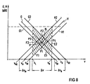
- FIGS. 6 to 8 show exemplary embodiments with the aid of diagrams how the logarithmic gain A of the amplifier device 2 can be controlled by varying the logarithmic transfer functions G and H of the two transfer elements 3 and 4.
- the decimal logarithmic amplification or transfer function that is common in electronics is described without restriction of generality
- a / dB 20 log (
- G / dB 20 log (
- ) H / dB 20 log (
- ) with the logarithm log: log 10 used for base 10.
- the transmission parameter ⁇ G corresponds to the value of ⁇ at which the elongated edge E intersects the abscissa.
- the edge E of the logarithmic transfer function G is kept constant during the operation of the amplifier device 2.
- the logarithmic transfer function H of the second transfer element 4 has a flank F which rises linearly with increasing ⁇ in accordance with the relationship (3b) with the gradient + m> 0 and which, from a certain functional limit value ⁇ 3, into a substantially constant part of the logarithmic transfer function H. transforms.
- This logarithmic transfer function H corresponds to the characteristic curve of a high pass as a transfer element 4.
- the edge F of the logarithmic transfer function H can now be shifted between two edges labeled F1 and F2 of two corresponding logarithmic transfer functions H1 and H2 with the same slope + m.
- the transfer parameter ⁇ H of the logarithmic transfer function H is varied in the interval limited by the two transfer parameters ⁇ H1 and ⁇ H2 of the two logarithmic transfer functions H1 and H2 with ⁇ H1 ⁇ H2 .
- the transmission parameters ⁇ H , ⁇ H1 and ⁇ H2 correspond to the values of ⁇ at which the extended flank F, F1 and F2 intersect the abscissa.
- the associated logarithmic transfer function H, H1 or H2 assumes a predetermined value, for example again 0 dB.
- the slope of the logarithmic transfer function H defined by the transfer parameter + m remains unchanged when the edge F is shifted.
- the flank F of the logarithmic transfer function H is in the hatched area over a functional value range ⁇ lying between the function limit value ⁇ 0 of the logarithmic transfer function G of the low pass as the left function value ⁇ L and the smallest function limit value ⁇ 1 of the logarithmic transfer function H of the high pass as the right function value ⁇ R Area displaceable relative to the edge E of the logarithmic transfer function G.
- the intersection P between the two edges E and F lies on the edge E between the two extreme intersections P1 of the edge F1 with the edge E and P2 of the edge F2 with the edge E.
- the logarithmic gain A of the amplifier device 2 can be graphically a double value one of the two logarithmic transfer functions G or H can be determined at this intersection point P.
- the maximum value A max of the logarithmic gain A corresponds to the intersection P1, the minimum value A min, however, to the intersection P2.
- the logarithmic transfer function H is now kept constant with the edge F with a positive slope (positive edge), while the logarithmic transfer function G is varied with the edge E with a negative slope (negative edge).
- the transfer parameter f H of the logarithmic transfer function H thus remains constant.
- the transfer parameter f G of the logarithmic transfer function G is controlled between the two transfer parameters f G2 and f G1 by two logarithmic transfer functions G2 and G1 with f G2 ⁇ f G1 .
- the edge E of the logarithmic transfer function G can thus be shifted with an unchanged slope m between the two edges E2 and E1 of the two logarithmic transfer functions G2 and G1 in a frequency range ⁇ f between a left corner frequency f L and a right corner frequency f R with f L ⁇ f R.
- the variation range of the edge E over the frequency range ⁇ f is hatched again.
- intersection P of the two flanks E and F varies between the intersection P2 of the edge E2 with the edge F and the intersection P1 of the edge E1 with the edge F.
- the resulting logarithmic gain A of the amplifier device 2 again corresponds to twice the logarithmic value Transfer function G or H at the intersection P.
- the logarithmic transfer function G can again be implemented with a transfer element 3 with a low-pass character.
- a variation ⁇ f G of the transmission parameter f G from f G2 to f G1 then also corresponds to a variation of the cutoff frequency of the low pass from f 2 to f 1 .
- the logarithmic transfer function H shown has a continuous edge F and can be implemented, for example, with a differentiator in the transfer element 4.
- the edges E and F of both logarithmic transfer functions G and H can now be shifted within the predetermined function value interval ⁇ .
- the transmission parameter ⁇ G of the logarithmic transmission function G of the first transmission element 3 is controlled in the variation interval limited by the two transmission parameters ⁇ G1 and ⁇ G2 of the two logarithmic transmission functions G1 and G2 with ⁇ G1 ⁇ G2 .
- the corresponding variation ranges of the flanks E and F over the interval ⁇ are hatched in each case.
- the intersection P of the two flanks E and F lies in the double-hatched, parallelogram-shaped area 15 with the four corner points P1, P2, P3 and P4.
- the vertex P1 is the intersection of the two flanks E1 and F1
- the vertex P2 is the intersection of the flanks E2 and F2
- the vertex P3 is the intersection of the flanks E1 and F2
- the vertex P4 is the intersection of the flanks E2 and F1.
- the variation ⁇ A of the gain A when the two transfer parameters ⁇ G and ⁇ H are varied is therefore equal to the sum of the individual variations ⁇ A according to the equations (7 ) or (6).
- the gain variation ⁇ A when shifting both flanks E and F by changing their associated transmission parameter ⁇ G or ⁇ H is twice as large as with variation of only one transmission parameter ⁇ G or ⁇ H , ie only when shifting an edge E or F.
- a transmission link with a positive edge such as the edge F in FIGS. 6 to 8 can preferably with the help of an nth order high pass with n ⁇ 1, one Differentiator or a preemphasis become.
- a transmission link with a negative edge like contains, for example, the edge E in FIGS. 6 to 8 preferably a low-pass n-th order with n ⁇ 1 Integrator or a de-emphasis element.
- each Transmission link preferably comprises at least in each case an amplifier for adjusting the absolute size of the associated transfer function.
- Amplifier device 2 also has at least one amplifier one that is frequency-independent at least in the frequency range ⁇ f Gain included, the electrical in series to the two Transmission elements 3 and 4 is switched.
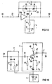
- the examples given for the transmission elements 3 and 4 The amplifier device 2 are numerous to the person skilled in the art known from embodiments. 9 to 14 show simple basic circuits for such transmission elements. All transmission elements shown contain a negative feedback Amplifier 20 with one input 20A and one Output 20B and a capacitive component 23. The input the transmission link corresponds to point 40, and the output of the transmission link corresponds to point 50. The Node 50 is at output 20B of amplifier 20 electrically connected.
- the input 20A of the amplifier 20 is connected to the output 20B of the amplifier 20 via a first electrical resistor 21 fed back.
- a minus sign at the input 20A of the amplifier 20 should indicate that the fed back part of the output signal the input signal reduced, i.e. there is negative feedback.
- An input signal at the input 40 of the high pass is via a series connection a second electrical resistor 22 and controllable capacitive component 23 to the input 20A of the amplifier 20 switched.
- the cutoff frequency of the high pass is now proportional to 1 / (RC) with the size R of the second electrical resistance 22 and the capacitance C of the capacitive component 23.
- a n-th order high pass n> 1 can be done simply by connecting n high passes in series first order.
- the slope of the rising corresponds to the positive edge of the n-th order high pass the n-fold slope of the positive flank of the high pass first order.
- the gain variation can thus be ordered for a transmission element ⁇ A of the amplifier device 2 accordingly multiply.
- FIG. 10 shows an embodiment of a differentiating element (Differentiator).
- the output 20B of the amplifier 20 is with electrically connected to the input 20A via the resistor 21. between these negative feedback input 20 A of the amplifier and the input 40 of the differentiator is capacitive Component 23 switched.
- This differentiator is obtained from the basic circuit for the high-pass filter shown in FIG. 9 Omission of the second resistor 22.
- the differentiator has no cutoff frequency.
- the output 20B of the Amplifier 20 again through the first resistor 21 with the Input 20A of amplifier 20 is fed back.
- the entrance 40 of the pre-emphasis element is now via a parallel connection of the second resistor 22 and the capacitive component 23 with electrically connected to the input 20A of the amplifier 20.
- the cutoff frequency of the pre-emphasis element is proportional to 1 / (RC), where R is the ohmic resistance of the second resistor 22 and C the electrical capacitance of the capacitive Component 23 are.
- FIG. 12 shows an embodiment of a low pass first Order shown.
- the output 20B of the amplifier 20 is via a parallel connection of the first resistor 21 and the capacitive component 23 with the input 20A of the amplifier 20 electrically connected.
- the input 40 of the low pass is via the second resistor 22 to the input 20A of the Amplifier 20 electrically connected.
- the cutoff frequency of the Low pass is proportional to 1 / (RC) with the size R of the first electrical resistance 21 and the capacitance C of the capacitive component 23.
- a n-th order low pass n> 1 can be done simply by connecting n low passes in series first order.
- the slope of the falling negative edge of the n-th order low pass corresponds to the n-fold slope of the negative edge of the First order low pass.
- FIG. 13 shows an embodiment of an integrating element (Integrators) illustrates. Output 20B and input 20A of the amplifier 20 are via the capacitive component 23 electrically coupled. In front of the input 20A of the amplifier 20, the resistor 22 is switched. The integrator 13 can by omitting the resistor 21 in the transmission element 12 can be obtained. A cut-off frequency does not have the integrator.
- FIG 14 shows a basic circuit of a Deemphasis limb as a transmission limb.
- the input 20A of the amplifier 20 is also via the second resistor 22 to the input 40 of the De-emphasis member electrically connected.
- the cutoff frequency of the The emphasis element is proportional to 1 / (RC) with the ohmic Resistor R of the first resistor 21 and the capacitor C. of the capacitive component 23.
- control means 5 are provided, which at least one capacitive component 23 each to be controlled Control the transmission element accordingly.
- the amplifier device 2 preferably each have a capacitance diode provided to which one of the control means 5 variable reverse voltage can be applied as a control voltage.
- capacitance diodes have precisely defined characteristics of their capacity depending on the reverse voltage applied.
- different converter elements 1 of an array for example in one embodiment 2 shows good synchronism properties.
- controllable capacitive component 23 also a normally-off field-effect transistor be provided on its source-drain path a control voltage is applied and its source and gate are electrically short-circuited. The capacity between source and drain is via the control voltage varied.
- a particular advantage of a capacitive control of the gain the amplifier device 2 in one of the described Embodiments is the low power dissipation such control.
- FIG. 15 shows an embodiment of a low pass according to FIG. 12, in which the controllable capacitive component 23 comprises two capacitance diodes 24 and 25 connected in series.
- the control means 5 apply a control voltage U C to the two capacitance diodes 24 and 25 via an electrical control line 8, for example, in the reverse direction.
- the control means 5 preferably contain a series resistor 52 and a control voltage source 51, which provides the control voltage U C.
- the control voltage U C is preferably selected such that neither of the two capacitance diodes 24 or 25 becomes conductive over the intended modulation range of the amplifier 20.
- Control means 5 one for both transmission elements 3 and 4 in common provided control voltage source included with the controllable capacitive components of both transmission elements 3 and 4 is connected.
- the 16 shows an embodiment of an amplifier device 2 with the two transmission elements 3 and 4 common control means 5.
- the first transmission element 3 contains a resistor 16, a pin diode 17 and a capacitor 18.
- the second transmission element 4 contains at least one bipolar transistor 19 as Amplifier and a negative feedback circuit for this at least one amplifier, which contains at least one capacitance diode as controllable capacitive component 23.
- the base B of the bipolar transistor 19 is preferably connected via a capacitance 49 and via the first transmission element 3 to the input 2A of the amplifier device 2.
- the collector C of the bipolar transistor 19 is connected to the output 2B of the amplifier device 2 via a capacitance 47.
- a positive supply voltage is present at the collector C of the bipolar transistor 19 via a series resistor 46.
- Emitter EM of the bipolar transistor 19 is a negative emitter voltage -U e via a series resistor 48.
- the signs of the two fixed voltages + U 0 and -U e apply to an npn transistor 19 and are of course interchangeable for a pnp transistor.
- a capacitance diode as controllable capacitive component 23 is now connected between the emitter EM of the bipolar transistor 19 and a control voltage source as the control means 5.
- the control means 5 apply a control voltage U C to the capacitance diode 23 operated in the reverse direction to control the capacitance of the capacitance diode 23.
- the frequency response of the transmission element 4 is a pre-emphasis element. Its thus positive edge can be shifted by changing the control voltage U C.
- Another capacitor 45 is connected to zero potential between the capacitor 49 and the bipolar transistor 19 in order to fix the base potential at the base B of the transistor 19.
- the control means 5 are also connected to the first transmission element 3.
- the control voltage U C is applied to a circuit point between the pin diode 17 and the capacitor 18 via the resistor 16.
- the series circuit of capacitance 18 and pin diode 17 is connected between the input 2A of the amplifier device 2 and zero potential.
- the first transmission element 3 forms, together with the internal resistance of the converter element 1, a low-pass filter with regard to its frequency response.
- the resistance of the pin diode 17 can be controlled by the control voltage U C of the control means 5.
- the resistance of the pin diode 17 also changes the cutoff frequency of the low pass formed with the first transmission element 3. By controlling the control voltage U C , the negative edge of the first transmission element 3 can therefore be shifted in addition to the positive edge of the second transmission element 4.
- amplifier devices have 2 in the embodiment according to FIG. 16 for arrays of converter elements 1 required good synchronization properties.
- the pin diode 17 is indeed in the forward direction operated, but are to control their resistance because of the comparatively high internal resistance of the converter element 1 only relatively low currents, typically less than 80 ⁇ A required.
- the associated maximum power loss is typically only a few 100 ⁇ W. Because of Transmission element 3 with the pin diode 17, the received signals S are weakened, is sufficient for the negative feedback bipolar Transistor 19 already has a low quiescent current not more than 100 ⁇ A. The power loss of the entire Amplifier device 2 is therefore very small.
- a gain variation according to FIG. 8 can be realized with the embodiment shown in FIG.
- the minimum gain A min and thus the modulation and dynamics of the amplifier device 2 can be determined by setting the maximum control voltage U C to be applied.
- bipolar transistor 19 instead of only one bipolar transistor 19 as an amplifier can also be a broadband cascode circuit of several bipolar transistors can be provided.
- the amplifier device 2 can in a not shown Embodiment also only one between input 2A and output 2B switched transmission element 3 or 4 in one of the above Embodiments with the at least one capacitive component 23 included.
- the amplifier device 2 is indeed on compensation the frequency response of the capacitive control of the gain A * or A omitted in the converter head 9, but can this frequency response also from a downstream signal processing Getting corrected.
- the amplifier device 2 in particular bipolar Transistors, field effect transistors, in particular MOSFETs, or also integrated operational amplifiers can be used. These three types of amplifiers are particularly suitable for Integration with an array of converter elements 1 in the converter head 9th
Description
Die Erfindung bezieht sich auf einen Ultraschallwandlerkopf und ein Ultraschallgerät mit einem solchen Wandlerkopf. Der Ultraschallwandlerkopf umfaßt wenigstens ein Wandlerelement, das Ultraschallsignale empfängt und in elektrische Empfangssignale umwandelt, sowie eine Verstärkereinrichtung, die die Empfangssignale des Wandlerelements elektrisch verstärkt. Ein solcher Ultraschallwandlerkopf ist aus der EP-A-0 600 654 bekannt.The invention relates to an ultrasonic transducer head and an ultrasound device with such a transducer head. The Ultrasonic transducer head comprises at least one transducer element, which receives ultrasound signals and into electrical reception signals converts, as well as an amplifier device that the Received signals of the converter element are electrically amplified. On such an ultrasonic transducer head is from EP-A-0 600 654 known.
Es sind Ultraschallgeräte zum Abbilden von Objekten mit Ultraschall mit Hilfe der Puls-Echo-Methode bekannt, die hauptsächlich in der Medizin zum Abbilden von Gewebe und in der zerstörungsfreien Werkstoffprüfung eingesetzt werden. Bei diesen bekannten Ultraschallgeräten wird ein Wandlerkopf (Applikator) über das abzubildende Objekt geführt. Der Wandlerkopf enthält wenigstens ein piezoelektrisches Wandlerelement, im allgemeinen jedoch eine Vielzahl von Wandlerelementen, die ein lineares oder zweidimensionales Array bilden. Die Wandlerelemente im Wandlerkopf werden in einem Sendebetrieb des Ultraschallgeräts durch elektrische Sendepulse eines Senders zu hochfrequenten Schwingungen angeregt und erzeugen einen auf das Objekt gerichteten Ultraschallpuls. Dieser Ultraschallpuls wird in dem Objekt beispielsweise an Grenzflächen zwischen zwei Medien unterschiedlicher akustischer Impedanz reflektiert. In einem Empfangsbetrieb des Systems werden die zum Wandlerkopf zurückreflektierten Ultraschall-Echopulse von den Wandlerelementen in entsprechende elektrische Empfangssignale umgewandelt. Diese Empfangssignale werden vom Wandlerkopf über entsprechende Signalkabel zu einem Hauptgerät (main frame) übertragen. Im Hauptgerät werden die übertragenen Empfangssignale jedes Wandlerelements von einem diesem Wandlerelement zugeordneten Vorverstärker verstärkt. Die verstärkten Empfangssignale werden einer Signalverarbeitungseinheit im Hauptgerät zum Auswerten der Informationen über das abgebildete Objekt zugeführt.There are ultrasound devices for imaging objects with Ultrasound using the pulse-echo method is known mainly in medicine for imaging tissue and in non-destructive material testing. at These known ultrasound devices become a transducer head (Applicator) over the object to be imaged. The converter head contains at least one piezoelectric transducer element, but generally a variety of transducer elements, that form a linear or two-dimensional array. The converter elements in the converter head are in a transmission mode of the ultrasound device through electrical transmission pulses of a transmitter excited to high frequency vibrations and generate an ultrasound pulse directed at the object. This ultrasound pulse is applied to the object, for example Interfaces between two media of different acoustic Impedance reflected. In a receiving operation of the system become the ultrasonic echo pulses reflected back to the transducer head from the transducer elements to corresponding ones electrical received signals converted. These receive signals are converted from the converter head via appropriate signal cables transmitted to a main frame. Be in the main unit the transmitted received signals of each transducer element from a preamplifier assigned to this converter element strengthened. The amplified received signals become one Signal processing unit in the main unit for evaluating the Information about the depicted object is supplied.
Ein Problem bei solchen Ultraschallgeräten ist die hohe Dynamik der Empfangssignale während des Empfangsbetriebs. Zu Beginn des Empfangsbetriebs sind die Signalamplituden der empfangenen Echopulse noch vergleichsweise hoch, nehmen dann aber wegen der Dämpfung innerhalb des Objekts mit zunehmender Dauer des Empfangsbetriebs immer mehr ab. Zum Ausgleich der durch die Dämpfung im Objekt bewirkte Signalabschwächung werden im allgemeinen im Hauptgerät steuerbare Verstärker mit einer laufzeitabhängig gesteuerten Verstärkung (Time-gaincompensation-amplifiers = TGC amplifiers) vorgesehen. Ein derartiges Hauptgerät wird beispielsweise in der US-A-4,445,379 beschrieben.A problem with such ultrasound devices is the high dynamics of the reception signals during reception operation. To The signal amplitudes of the receive mode begin received echo pulses are still relatively high, then take but because of the attenuation within the object with increasing Duration of reception operation more and more. To balance the attenuation caused by the attenuation in the object generally controllable amplifiers in the main unit a time-dependent gain control (time-gain compensation-amplifiers = TGC amplifiers). On such main unit is, for example, in the US-A-4,445,379.
Ein weiteres Problem stellen die Impedanzunterschiede zwischen den vergleichsweise hochohmigen Wandlerelementen und den niederohmigen Signalkabeln und die daraus resultierende Belastung der Wandlerelemente als Signalquellen dar. Zur besseren Impedanzanpassung ist aus US-A-4,489,729 bekannt, im Wandlerkopf für jedes Wandlerelement einen linearen Vorverstärker mit fest eingestellter Verstärkung zu integrieren. Dieser bekannte lineare Vorverstärker enthält einen Operationsverstärker, dessen Ausgang mit einem Eingang über eine Parallelschaltung aus einem Festwiderstand einerseits und einer Reihenschaltung zweier Kondensatoren andererseits (Tiefpaßschaltung) rückgekoppelt ist. Stellt man die konstante Verstärkung solcher Vorverstärker klein ein, so ist der Signal-Rausch-Abstand für schwache Empfangssignale entsprechend klein. Bei großer konstanter Verstärkung der Vorverstärker können dagegen hohe Empfangssignalamplituden verzerrt werden. Bei Verwendung eines Vorverstärkers mit fest eingestellter Verstärkung ist deshalb der Dynamikbereich des Ultraschallgeräts vergleichsweise klein. Another problem is the impedance mismatch between the relatively high impedance transducer elements and the low-signal cables, and the resultant loading of the transducer elements as signal sources represent For a better impedance matching is known from US -. A - 4,489,729 is known, in the transducer head for each transducer element is a linear preamplifier with a fixed gain to integrate. This known linear preamplifier contains an operational amplifier, the output of which is fed back with an input via a parallel circuit comprising a fixed resistor on the one hand and a series connection of two capacitors on the other hand (low-pass circuit). If the constant amplification of such preamplifiers is set to be small, the signal-to-noise ratio for weak received signals is correspondingly small. With large constant amplification of the preamplifiers, however, high received signal amplitudes can be distorted. When using a preamplifier with a fixed gain, the dynamic range of the ultrasound device is therefore comparatively small.
Aus EP-A-0 600 654 ist ein Ultraschallgerät zum Abbilden eines Objekts bekannt, bei dem jedem Wandlerelement im Wandlerkopf zusätzlich zu einem Vorverstärker mit konstanter Verstärkung ein Verstärker mit steuerbarer Verstärkung (variable gain amplifier) zugeordnet ist. Der Vorverstärker mit fest vorgegebener Verstärkung ist elektrisch zwischen das Wandlerelement und den steuerbaren Verstärker geschaltet. Der Ausgang des steuerbaren Verstärkers ist mit einem Gegentaktemitterfolger als Impedanzwandler gebildet und ist mit dem zugehörigen Signalkabel elektrisch verbunden, das die verstärkten Empfangssignale zu einem Hauptgerät überträgt. Die Eingangsimpedanz des Vorverstärkers ist der hohen Impedanz des Wandlerelements angepaßt, während die Ausgangsimpedanz des Gegentaktemitterfolgers der niedrigeren Impedanz des Signalkabels angepaßt ist. Im Hauptgerät werden die verstärkten Empfangssignale zum Aufbau eines Bildes des Objekts herangezogen. Der steuerbare Verstärker wird vom Hauptgerät über zusätzliche Leitungen im Signalkabel mit Steuersignalen (TGC control signals) zum Steuern der Verstärkung des steuerbaren Verstärkers angesteuert, um laufzeitabhängige Dämpfungen zu kompensieren. Bei diesem bekannten Ultraschallgerat sind somit die steuerbaren Kompensationsverstärker (TGC amplifiers) im Wandlerkopf integriert.An ultrasound device for imaging an object is known from EP-A-0 600 654 , in which each transducer element in the transducer head is assigned an amplifier with controllable gain (variable gain amplifier) in addition to a preamplifier with constant gain. The pre-amplifier with a predetermined gain is electrically connected between the converter element and the controllable amplifier. The output of the controllable amplifier is formed with a push-pull emitter follower as an impedance converter and is electrically connected to the associated signal cable, which transmits the amplified received signals to a main device. The input impedance of the preamplifier is matched to the high impedance of the transducer element, while the output impedance of the push-pull emitter follower is matched to the lower impedance of the signal cable. In the main device, the amplified received signals are used to build up an image of the object. The controllable amplifier is controlled by the main unit via additional lines in the signal cable with control signals (TGC control signals) for controlling the amplification of the controllable amplifier in order to compensate for time-dependent damping. In this known ultrasound device, the controllable compensation amplifiers (TGC amplifiers) are thus integrated in the transducer head.
Die steuerbaren Verstärker in diesem aus EP-A-0 600 654 bekannten Wandlerkopf funktionieren nach dem Prinzip eines Steilheitsmultiplizierers, der beispielsweise aus Tietze, Schenk: "Halbleiterschaltungstechnik", 9. Auflage, 1990, Springer Verlag, S. 350 bekannt ist. Der Ruhestrom der gesamten Schaltung muß so bemessen sein, daß auch das Ultraschallempfangssignal mit der höchsten Amplitude verzerrungsfrei übertragen wird. Die steuerbaren Verstärker beim aus EP-A-0 600 654 bekannten Ultraschallgerät weisen daher eine vergleichsweise hohe Verlustleistung auf.The controllable amplifiers in this converter head known from EP - A - 0 600 654 function according to the principle of a steepness multiplier, which is known, for example, from Tietze, Schenk: "Semiconductor circuit technology", 9th edition, 1990, Springer Verlag, p. 350 . The quiescent current of the entire circuit must be dimensioned such that the ultrasound received signal with the highest amplitude is also transmitted without distortion. The controllable amplifiers in the ultrasound device known from EP - A - 0 600 654 therefore have a comparatively high power loss.
Es ist ein Operationsverstärker mit einer steuerbaren Verstärkung bekannt, bei dem ein von einer kontinuierlich oder digital steuerbaren Steuerspannungsquelle steuerbarer Feldeffekttransistor (FET) in eine Gegenkopplungsschaltung für den Operationsverstärker geschaltet ist. Für den FET als steuerbaren Widerstand ist zusätzlich eine Rückkopplungsschaltung mit einem weiteren Operationsverstärker zum Linearisieren des elektrischen Widerstandes des FET vorgesehen. Auch kann der FET mit einer Gegenkopplung zum Vergrößern seines Dynamikbereichs beschaltet sein ("Application Note 200-1, Designer's Guide for 200 Series Op Amps" der Firma Comlinear Corporation, November 1984). FETs als steuerbare Widerstände benötigen zwar keine Steuerleistung, weisen jedoch vergleichsweise hohe Toleranzen in ihren Kennlinien auf.An operational amplifier with a controllable amplification is known, in which a field effect transistor (FET) controllable by a continuously or digitally controllable control voltage source is connected to a negative feedback circuit for the operational amplifier. A feedback circuit with a further operational amplifier for linearizing the electrical resistance of the FET is additionally provided for the FET as a controllable resistor. The FET can also be connected to a negative feedback to increase its dynamic range ( "Application Note 200-1, Designer's Guide for 200 Series Op Amps" from Comlinear Corporation, November 1984 ). FETs as controllable resistors do not require any control power, but they have comparatively high tolerances in their characteristic curves.
Bei zweidimensionalen Arrays von Ultraschallwandlerelementen ist eine große Anzahl (typischerweise 5000) von Vorverstärkern in dem Wandlerkopf in einem deutlich kleineren Volumen zu integrieren als bei eindimensionalen Arrays. Der Leistungsverbrauch der Vorverstärker muß deshalb im allgemeinen deutlich kleiner sein als bei einem eindimensionalen Array, um eine Überhitzung zu vermeiden. Aus dem gleichen Grund stellt auch die Verlustleistung der integrierten Verstärker in einem aus der genannten EP-A-0 600 654 bekannten Ultraschallwandlerkopf ein Problem dar.With two-dimensional arrays of ultrasonic transducer elements, a large number (typically 5000) of preamplifiers must be integrated in the transducer head in a significantly smaller volume than with one-dimensional arrays. The power consumption of the preamplifiers must therefore generally be significantly lower than with a one-dimensional array in order to avoid overheating. For the same reason, the power loss of the integrated amplifiers in an ultrasonic transducer head known from EP-A-0 600 654 mentioned is also a problem.
Der Erfindung liegt deshalb die Aufgabe zugrunde, einen Ultraschallwandlerkopf mit wenigstens einem Wandlerelement und mit einer steuerbaren Verstärkereinrichtung für jedes Wandlerelement sowie ein Ultraschallgerät mit einem solchen Wandlerkopf anzugeben, bei denen die Verstärkung jeder Verstärkereinrichtung steuerbar ist und zugleich die Verlustleistung jeder Verstärkereinrichtung geringgehalten wird. Bei einem eindimensionalen oder zweidimensionalen Array von Wandlerelementen im Wandlerkopf sollen die den Wandlerelementen jeweils zugeordneten Verstärkereinrichtungen außerdem gute Gleichlaufeigenschaften aufweisen.The invention is therefore based on the object of an ultrasonic transducer head with at least one transducer element and with a controllable amplifier device for each transducer element and an ultrasound device with one Specify transducer head where the gain of each amplifier device is controllable and at the same time the power loss each amplifier device is kept low. at a one-dimensional or two-dimensional array of transducer elements in the transducer head they should be the transducer elements each associated amplifier devices also good Have synchronism properties.
Diese Aufgabe wird gemäß der Erfindung gelöst mit den Merkmalen des Anspruchs 1 bzw. des Anspruchs 12. This object is achieved according to the invention with the features of claim 1 or claim 12.
Die Erfindung beruht auf der Überlegung, die Verstärkung der Verstärkereinrichtung durch Steuern einer Kapazität zu steuern. Eine solche kapazitive Steuerung weist einen praktisch vernachlässigbaren Stromverbrauch auf. Die Verstärkereinrichtung enthält ausgehend von dieser Überlegung wenigstens ein kapazitives Bauelement, dessen Kapazität steuerbar ist und die Verstärkung der Verstärkereinrichtung bestimmt.The invention is based on the consideration, the amplification of the Control amplifier device by controlling a capacitance. Such a capacitive control is practical negligible power consumption. The amplifier device based on this consideration, contains at least one capacitive component, the capacity of which is controllable and determines the gain of the amplifier device.
Ausgestaltungen und Weiterbildungen des Ultraschallwandlerkopfs und des Ultraschallgeräts gemäß der Erfindung ergeben sich aus den vom Anspruch 1 bzw. vom Anspruch 12 jeweils abhängigen Ansprüchen.Refinements and developments of the ultrasonic transducer head and the ultrasound device according to the invention depend on those of claim 1 and claim 12, respectively Claims.
Als steuerbares kapazitives Bauelement ist vorzugsweise eine Kapazitätsdiode vorgesehen. Kapazitätsdioden sind über eine in Sperrichtung angelegte Steuerspannung praktisch verlustleistungsfrei steuerbar und weisen genau reproduzierbare Kennlinien auf.A controllable capacitive component is preferably one Capacitance diode provided. Capacitance diodes are over one control voltage applied in the reverse direction is practically lossless controllable and precisely reproducible Characteristic curves on.
In einer vorteilhaften Ausführungsform ist das wenigstens eine kapazitive Bauelement in eine Gegenkopplungsschaltung für wenigstens einen Verstärker geschaltet.In an advantageous embodiment, this is at least one capacitive component in a negative feedback circuit for switched at least one amplifier.
Eine besonders vorteilhafte Ausführungsform beruht auf der weiteren Überlegung, das elektrische Empfangssignal des Wandlerelements in der Verstärkereinrichtung nacheinander zwei Übertragungsgliedern mit unterschiedlich frequenzabhängigen Übertragungsfunktionen zuzuführen und die beiden Übertragungsfunktionen dabei so zu wählen oder so einzustellen, daß sich ihre Frequenzabhängigkeiten in einem vorgegebenen Frequenzbereich der Empfangssignale im wesentlichen kompensieren und die Amplitude des verstärkten Ausgangssignals der Verstärkereinrichtung gegenüber der Amplitude des Eingangssignals eine im wesentlichen frequenzunabhängige Verstärkung aufweist. Die Verstärkung für das elektrische Empfangssignal wird dann durch Verändern der Frequenzabhängigkeit der beiden Übertragungsfunktionen in dem vorgegebenen Frequenzbereich gesteuert. Aufbauend auf dieser Überlegung enthalt die Verstärkereinrichtung in dieser Ausführungsform zwei elektrische Übertragungsglieder mit jeweils einer frequenzabhängigen Übertragungsfunktion. Die Übertragungsfunktion ist dabei definiert als Verhältnis der Amplitude des Ausgangssignal zur Amplitude des Eingangssignals des jeweiligen Übertragungsglieds. Die beiden Übertragungsglieder sind zwischen einen Eingang der Verstärkereinrichtüng zum Anlegen des zu verstärkenden elektrischen Empfangssignals und einen Ausgang der Verstärkereinrichtung zum Abgreifen des verstärkten elektrischen Empfangssignals in Reihe geschaltet. Wenigstens eines der beiden Übertragungsglieder enthält das wenigstens eine steuerbare kapazitive Bauelement. Die Frequenzabhängigkeiten der Übertragungsfunktionen der beiden Übertragungsglieder sind so gewählt, daß die beiden entsprechenden logarithmischen Übertragungsfunktionen im Bereich jeweils einer Flanke im wesentlichen linear abhängig von einer bijektiven Funktion der Frequenz sind. Die logarithmische Übertragungsfunktion ist dabei proportional zum Logarithmus des Betrags der im allgemeinen komplexen Übertragungsfunktion zu einer vorgegebenen reellen Basis. Die logarithmische Übertragungsfunktion eines der beiden Übertragungsglieder weist eine positive Flanke mit einer positiven Steigung auf, während die logarithmische Übertragungsfunktion des anderen Übertragungsglieds eine negative Flanke aufweist mit einer negativen Steigung. Die Steigungen der beiden Flanken der logarithmischen Übertragungsfunktionen sind betragsmäßig wenigstens annähernd gleich gewählt. Die Flanken der beiden logarithmischen Übertragungsfunktionen sind nun relativ zueinander innerhalb des Frequenzbereichs der Empfangssignale verschiebbar. Durch Verschieben der Flanken gegeneinander wird die Verstärkung der Verstärkereinrichtung gesteuert.A particularly advantageous embodiment is based on the further consideration, the electrical reception signal of the transducer element two in succession in the amplifier device Transmission links with different frequency-dependent Feed transfer functions and the two transfer functions to choose or adjust so that their frequency dependencies in a given frequency range substantially compensate for the received signals and the amplitude of the amplified output signal of the amplifier device versus the amplitude of the input signal an essentially frequency-independent gain having. The gain for the electrical received signal is then changed by changing the frequency dependence of the two Transfer functions in the specified frequency range controlled. Building on this consideration, the amplifier device contains in this embodiment two electrical Transmission elements, each with a frequency-dependent Transfer function. The transfer function is included defined as the ratio of the amplitude of the output signal to the Amplitude of the input signal of the respective transmission element. The two transmission links are between one Input of the amplifier device for applying the one to be amplified electrical received signal and an output of Amplifier device for tapping the amplified electrical Received signal connected in series. At least one of the two transmission elements contains at least one controllable capacitive component. The frequency dependencies the transfer functions of the two transfer elements are chosen so that the two corresponding logarithmic Transfer functions in the area of one edge each essentially linear depending on a bijective function of the frequency. The logarithmic transfer function is proportional to the logarithm of the amount in general complex transfer function to a given real basis. The logarithmic transfer function one of the two transmission links has a positive one Slope with a positive slope while the logarithmic Transfer function of the other transmission link has a negative edge with a negative edge Pitch. The slopes of the two flanks of the logarithmic In terms of amount, transfer functions are at least chosen approximately the same. The flanks of the two logarithmic Transfer functions are now relative to each other slidable within the frequency range of the received signals. By moving the flanks against each other the Gain of the amplifier device controlled.
Das Ultraschallgerät enthält dazu Steuermittel, die wenigstens mit dem Übertragungsglied, das das kapazitive Bauelement enthält, in Wirkverbindung stehen. Die Steuermittel können nur eine Flanke zu kleineren oder größeren Frequenzen hin verschieben, während die andere Flanke unverändert bleibt, oder auch beide Flanken zugleich verschieben.For this purpose, the ultrasound device contains control means that at least with the transmission element that is the capacitive component contains, are in operative connection. The tax revenue can only flank to smaller or larger frequencies move towards it while the other flank remains unchanged remains, or shift both flanks at the same time.
Das Übertragungsglied mit der positiven Flanke (Flanke mit positiver Steigung) kann wenigstens ein Element aus der einen Hochpaß wenigstens erster Ordnung, einen Differentiator und ein Preemphasisglied umfassenden Gruppe von elektrischen Schaltungen oder Netzwerken enthalten. Das Übertragungsglied mit der negativen Flanke (Flanke mit negativer Steigung) kann wenigstens ein Element aus der einen Tiefpaß wenigstens erster Ordnung, einen Integrator und ein Deemphasisglied umfassenden Gruppe von elektrischen Schaltungen oder Netzwerken enthalten. Solche Übertragungsglieder können insbesondere mit gegengekoppelten Verstärkern realisiert werden.The transmission element with the positive edge (edge with positive slope) can be at least one element from one High pass at least first order, a differentiator and a pre-emphasis group of electrical Circuits or networks included. The transmission link with the negative edge (edge with negative slope) at least one element from the one low pass at least first Order, comprising an integrator and a de-emphasis member Group of electrical circuits or networks contain. Such transmission elements can in particular with negative feedback amplifiers can be realized.
Zur weiteren Erläuterung der Erfindung wird auf die Zeichnung Bezug genommen, in deren
- FIG 1
- ein Ultraschallwandlerkopf in einem prinzipiellen Aufbau
- FIG 2
- ein Ultraschallgerat mit einem Wandlerkopf in einem prinzipiellen Aufbau
- FIG 3
- eine Verstärkereinrichtung im Wandlerkopf mit einem gegengekoppelten Verstärker
- FIG 4
- ein prinzipieller Aufbau einer Verstärkereinrichtung im Wandlerkopf mit zwei Übertragungsgliedern,
- FIG 5
- eine typische Abhängigkeit der Verstärkung der Verstärkereinrichtung von der Frequenz der Empfangssignale in einem Diagramm,
- FIG 6
bis 8 - jeweils ein Ausführungsbeispiel zum Verschieben der Flanken der Übertragungsfunktionen der beiden Übertragungsglieder der Verstärkereinrichtung,
- FIG 9
bis 11 - jeweils eine Ausführungsform eines Übertragungsglieds mit positiver Flanke,
- FIG 12 bis 14
- jeweils eine Ausführungsform eines Übertragungsglieds mit negativer Flanke
- FIG 15
- eine Ausführungsform eines Übertragungsglieds mit zwei steuerbaren Kapazitätsdioden
- FIG 16
- eine Ausführungsform einer Verstärkereinrichtung im Wandlerkopf mit zwei besonderen Übertragungsgliedern und gemeinsamen Steuermitteln
- FIG. 1
- an ultrasonic transducer head in a basic structure
- FIG 2
- an ultrasound device with a transducer head in a basic structure
- FIG 3
- an amplifier device in the converter head with a negative feedback amplifier
- FIG 4
- a basic structure of an amplifier device in the converter head with two transmission elements,
- FIG 5
- a typical dependence of the amplification of the amplifier device on the frequency of the received signals in a diagram,
- 6 to 8
- an embodiment for shifting the edges of the transfer functions of the two transfer elements of the amplifier device,
- 9 to 11
- one embodiment of a transmission element with a positive edge,
- 12 to 14
- one embodiment of a transmission element with a negative edge
- FIG. 15
- an embodiment of a transmission link with two controllable capacitance diodes
- FIG 16
- an embodiment of an amplifier device in the converter head with two special transmission elements and common control means
Der in FIG 1 gezeigte, mit 9 bezeichnete Ultraschallwandlerkopf
enthalt wenigstens ein Wandlerelement 1 und eine Verstärkereinrichtung
2 zum Verstärken der Empfangssignale S des
Wandlerelements 1. An einen Eingang 2A der Verstärkereinrichtung
2 werden die Empfangssignale S des Wandlerelements 1 angelegt.
Die verstärkten Empfangssignale können an einem Ausgang
2B der Verstärkereinrichtung 2 abgegriffen werden und
sind mit S' bezeichnet.The ultrasonic transducer head shown in FIG. 1, designated 9
contains at least one converter element 1 and an
Zum Steuern ihrer im allgemeinen komplexen Verstärkung
A* = S'/S enthält die Verstärkereinrichtung 2 wenigstens ein
steuerbares kapazitives Bauelement 23. Die Verstärkung A* der
Verstärkereinrichtung 2 ist von der Kapazität C des steuerbaren
kapazitiven Bauelements 23 abhängig. Zum Steuern der
Kapazität C des kapazitiven Bauelements 23 und damit der Verstärkung
A* der Verstärkereinrichtung 2 ist das wenigstens
eine kapazitive Bauelement 23 über eine gestrichelt dargestellte
Wirkverbindungslinie 8 mit Steuermitteln 5 verbunden.
Die Wirkverbindung der Steuermittel 5 mit dem wenigstens
einen zu steuernden kapazitiven Bauelement 23 kann beispielsweise
über eine elektrische, optische, induktive oder auch
piezoelektrische Kopplung erfolgen. Die Wirkverbindungslinie
8 kann dann entsprechend mit einer elektrischen Verbindung
bzw. einem optischen Koppler bzw. einem induktiven Koppler
bzw. einem Piezokoppler gebildet sein. Die Steuermittel 5
sind im allgemeinen außerhalb des Wandlerkopfs 9 angeordnet,
können jedoch auch wenigstens teilweise im Wandlerkopf 9 integriert
sein.To control their generally complex gain
A * = S '/ S contains the
Als Wandlerelement 1 kann ein beliebiges piezoelektrisches Wandlerelement vorgesehen werden, insbesondere ein piezokeramisches Element. Das Wandlerelement 1 ist vorzugsweise Teil eines in FIG 1 nicht dargestellten Ultraschallarrays mit mehreren Wandlerelementen. Das Array kann ein lineares oder auch ein zweidimensionales, beispielsweise matrixförmiges Array sein. Solche Arrays sind im allgemeinen in einem Substrat durch Mikrostrukturierung integriert. Jedem Wandlerelement des Arrays ist dann eine steuerbare Verstärkereinrichtung zum Verstärken der Empfangssignale des Wandlerelements zugeordnet. Die Verstärkereinrichtungen sind zusammen mit den Wandlerelementen des Arrays im Wandlerkopf integriert.Any piezoelectric can be used as the transducer element 1 Transducer element are provided, in particular a piezoceramic Element. The transducer element 1 is preferably part of an ultrasound array (not shown in FIG. 1) with several Transducer elements. The array can be linear or also a two-dimensional, for example matrix-shaped array his. Such arrays are generally in a substrate integrated through microstructuring. Every converter element of the array is then a controllable amplifier device for Amplify the received signals of the transducer element. The amplifier devices are together with the transducer elements of the array integrated in the converter head.
Der Wandlerkopf 9 kann nur zum Empfangen von Ultraschall oder auch sowohl zum Senden als auch zum Empfangen von Ultraschall vorgesehen sein.The transducer head 9 can only be used to receive ultrasound or also for both sending and receiving ultrasound be provided.
Das Ultraschallgerät zum Abbilden eines - nicht dargestellten
- Objekts mit Ultraschall gemäß der FIG 2 enthält einen
Wandlerkopf 9 sowohl zum Senden als auch zum Empfangen von
Ultraschall mit einem Array von Wandlerelementen 1 und jeweils
einer steuerbaren Verstärkereinrichtung 2 für jedes
Wandlerelement 1. In einem Sendebetrieb des Ultraschallgeräts
wird das Objekt mit Ultraschallpulsen der Wandlerelemente 1
beschallt. Ein Sender 30 sendet dazu über Sendeleitungen 33
Sendepulse zum Ansteuern jedes Wandlerelements 1, die derart
beschaffen sind, daß die Wandlerelemente 1 zu Ultraschallschwingungen
angeregt werden. Die Einschaltdauer eines einzelnen
Sendepulses kann dabei im allgemeinen zwischen 50 ns
und 500 ns und vorzugsweise um etwa 150 ns gewählt werden,
und die Pulshöhe (Amplitude) der Sendepulse zwischen 50 und
150 V. Alle Wandlerelemente 1 des Arrays werden vorzugsweise
phasenverzögert von dem Sender 30 angesteuert zum Erzeugen
eines vorzugsweise fokussierbaren Ultraschallstrahls, der auf
das Objekt gerichtet wird (elektronischer Scan). Bei einem
Wandlerkopf mit nur einem einzelnen Wandlerelement 1 wird das
Objekt dagegen mechanisch abgetastet durch Bewegen des Wandlerelements
1 (mechanischer Scan). In einem Empfangsbetrieb
des Ultraschallgeräts werden die vom Objekt zu den Wandlerelementen
1 zurückreflektierten Ultraschallpulse in jedem
Wandlerelement 1 in elektrische Empfangssignale S umgewandelt.
Diese Empfangssignale S werden im Wandlerkopf 9 von der
zugehörigen Verstärkereinrichtung 2 verstärkt, und die verstärkten
Empfangssignale S' werden über Signalleitungen 34
signalverarbeitenden Mitteln 31 zum Aufbau eines Bildes des
Objekts zugeführt. Die Impedanzen der Verstärkereinrichtungen
2 sind vorzugsweise wenigstens annähernd an die Impedanzen
der zugeordneten Signalleitungen 34 angepaßt. Für jedes
Wandlerelement 1 ist vorzugsweise ein Duplexer 32 vorgesehen
zum Umschalten zwischen Sendebetrieb und Empfangsbetrieb. Ein
erster Teil 32A des Duplexers 32 verbindet im Sendebetrieb
das zugehörige Wandlerelement 1 mit dem Sender 30 und entkoppelt
im Empfangsbetrieb den Sender 30 sowohl von der
Verstärkereinrichtung 2 als auch von dem Wandlerelement 1.
Ein zweiter Teil 32B des Duplexers 32 verbindet dagegen das
Wandlerelement 1 im Empfangsbetrieb mit der Verstärkereinrichtung
2 und entkoppelt im Sendebetrieb die im allgemeinen
empfindliche Verstärkereinrichtung 2' zum einen von dem Sender
30 zum Schutz vor dessen Sendepulsen und zum anderen von dem
Wandlerelement 1. Das Wandlerelement 1 und die beiden Teile
32A und 32B des Duplexers 32 sind an einem gemeinsamen
Schaltpunkt elektrisch verbunden. Wenigstens der zwischen
Wandlerelement 1 und den Eingang 2A der zugeordneten Verstärkereinrichtung
2 angeordnete zweite Teil 32 B jedes Duplexers
32 ist mit dem Wandlerelement 1 und der Verstärkereinrichtung
2 im Wandlerkopf 9 integriert. Auch der erste Teil 32A kann
wie dargestellt im Wandlerkopf 9 angeordnet sein. Für den
Duplexer 32 können nicht dargestellte Steuerleitungen zum
Umschalten zwischen Sende- und Empfangsbetrieb vorgesehen
sein.The ultrasound device for imaging a - not shown
- Object with ultrasound according to FIG 2 contains one
Transducer head 9 for both sending and receiving
Ultrasound with an array of transducer elements 1 and each
a
Jede Verstärkereinrichtung 2 enthält mindestens ein steuerbares
kapazitves Bauelement 23. Jedes steuerbare kapazitve
Bauelement 23 ist über vorzugsweise eine gemeinsame elektrische
Steuerleitung 8 als Wirkverbindungslinie mit den
Steuermitteln 5 verbunden. Die kapazitiven Bauelemente 23
werden von einem gemeinsamen Steuersignal CS angesteuert zum
Steuern der Verstärkungen A* der Verstärkereinrichtungen 2.
Diese Ausführungsform mit einer gemeinsamen Ansteuerung aller
Verstärkereinrichtungen 2 ist besonders vorteilhaft bei im
wesentlichen zueinander identisch aufgebauten und ausgelegten
Wandlerelementen 1 und Verstärkereinrichtungen 2 im Wandlerkopf
9. Die Verstärkereinrichtungen 2 können aber auch jede
für sich über eine oder mehrere Steuerleitungen bzw. Wirkverbindungslinien
8 mit den Steuermitteln 5 in Wirkverbindung
stehen zum unabhängigen Steuern der Verstärkungen A* der
Verstärkereinrichtungen 2. Außerdem kann die Wirkverbindung
zwischen Verstärkereinrichtungen 2 und Steuermitteln 5 statt
auf elektrischem Wege auch wieder auf einem der anderen beschriebenen
Wege erfolgen.Each
Die Verstärkereinrichtung 2 enthält in einer vorteilhaften
Ausführungsform wenigstens einen Verstärker, dessen Eingang
mit dem Wandlerelement 1 verbunden ist und dessen Ausgang mit
dem Ausgang 2B der Verstärkereinrichtung 2 verbunden ist. Zusätzlich
ist eine Gegenkopplungsschaltung für den wenigstens
einen Verstärker vorgesehen. Bei nur einem Verstärker wird
der Ausgang des Verstärkers mit dessen Eingang verbunden. Ein
Teil des Ausgangssignals des Verstärkers wird zum Eingang zurückgeführt
und dem Eingangssignal des Verstärkers gegenphasig
überlagert, so daß das wirksame Eingangssignal abgeschwächt
wird. Bei mehreren hintereinandergeschalteten Verstärkern
kann eine Gegenkopplungsschaltung für jeden einzelnen
Verstärker vorgesehen sein oder eine Gegenkopplungsschaltung
über wenigstens zwei und vorzugsweise alle aufeinanderfolgenden
Verstärker oder eine Kombination aus solchen Einzel-
und Mehrfach-Gegenkopplungen vorgesehen sein. Bei einer
Gegenkopplung mehrerer hintereinandergeschalteter Verstärker
wird das Ausgangssignal des letzten Verstärkers mit dem Eingangssignal
des ersten Verstärkers gegengekoppelt. Die Gegenkopplungsschaltung
des wenigstens einen Verstärkers enthält
das wenigstens eine steuerbare kapazitive Bauelement 23. Eine
Änderung der Kapazität C des wenigstens einen kapazitiven
Bauelements 23 hat dann eine Änderung des Gegenkopplungsgrads
und damit der Verstärkung A* der Verstärkereinrichtung 2 zur
Folge.The
Ein erstes Ausführungsbeispiel für eine Verstärkereinrichtung
2 mit einem gegengekoppelten Verstärker ist in der FIG 3 dargestellt.
Als Verstärker ist ein Feldeffekttransistor 6 vorgesehen
mit einem Gate CG, einer Source SC und einer Drain D.
Das Gate CG des Feldeffekttransistors 6 ist mit dem Eingang
2A der Verstärkereinrichtung 2 verbunden. Die Source SC des
Feldeffekttransistors 6 ist mit einer Kapazitätsdiode als
kapazitivem Bauelement 23 verbunden. Die Drain D bildet den
Ausgang des Verstärkers und ist einerseits über eine Kapazität
27 mit dem Ausgang 2B der Verstärkereinrichtung 2 verbunden
sowie andererseits über einen Widerstand 26 mit einer
positiven Drainspannung U0. Die Kapazitätsdiode 23 ist über
eine Steuerleitung 8 mit einer Steuerspannungsquelle als
Steuermitteln 5 verbunden, die die Kapazitätsdiode 23 in
Sperrichtung mit einer Sperrspannung UC vorspannt. Durch die
Kapazitätsdiode 23 wird das Ausgangssignal des Feldeffekttransistors
6 teilweise auf dessen Eingangssignal gegengekoppelt.
Ändert man deshalb durch Steuern der Sperrspannung
UC die Kapazität C der Kapazitätsdiode 23, so verändert sich
der Gegenkopplungsgrad des Verstärkers 6 und damit die Verstärkung
A* der Verstärkereinrichtung 2. Allerdings ist die
Gegenkopplung mit dem kapazitiven Bauelement 23 und die Verstärkung
der Verstärkereinrichtung 2 wegen des Einflusses der
Kapazität C des kapazitiven Bauelements 23 frequenzabhängig,
im dargestellten Fall in Form eines Hochpaßverhaltens. Diese
Frequenzabhängigkeit kann aber bei der Signalauswertung der
verstärkten Empfangssignale S' berücksichtigt und korrigiert
werden. Ferner sind vorzugsweise noch ein Widerstand 29 zum
Festlegen des Gatepotentials am Gate CG des Feldeffekttransistors
6 und ein Widerstand 28 vorgesehen, der bewirkt,
daß an der Source SC ebenfalls das Ausgangssignal auftritt,
das zur Gegenkopplung verwendet wird.A first exemplary embodiment of an
In einer besonders vorteilhaften Ausführungsform der Verstärkereinrichtung
2 wird die Verstärkung A* der Verstärkereinrichtung
2 zwar durch Steuern der Kapazität C wenigstens
eines kapazitiven Bauelements 23, jedoch im wesentlichen
frequenzunabhängig gesteuert. Diese Ausführungsform wird
anhand der FIG 4 bis 16 näher beschrieben.In a particularly advantageous embodiment of the
In FIG 4 ist der prinzipielle Aufbau einer solchen Verstärkereinrichtung
2 mit frequenzunabhängiger Verstärkungssteuerung
gezeigt. Die Verstärkereinrichtung 2 umfaßt ein
erstes Übertragungsglied 3 mit einer im allgemeinen komplexen
Übertragungsfunktion G', ein zweites Übertragungsglied 4 mit
einer im allgemeinen komplexen Übertragungsfunktion H'. Das
erste Übertragungsglied 3 und das zweite Übertragungsglied 4
sind zwischen den Eingang 2A und den Ausgang 2B der Verstärkereinrichtung
2 elektrisch in Reihe geschaltet. Das zu verstärkende
elektrische Empfangssignal S des Wandlerelements 1
wird an den Eingang 2A der Verstärkereinrichtung 2 angelegt
und dem ersten Übertragungsglied 3 zugeführt. In dem ersten
Übertragungsglied 3 wird das Empfangssignal S mit der Übertragungsfunktion
G' des ersten Übertragungsgliedes 3 multipliziert.
Das erhaltene, mit der Übertragungsfunktion G' verstärkte
oder multiplizierte Empfangssignal G' * S wird nun
dem zweiten Übertragungsglied 4 zugeführt und von diesem mit
dessen Übertragungsfunktion H' verstärkt. Das mit beiden
Übertragungsfunktionen G' und H' beider Übertragungsglieder 3
und 4 multiplizierte Empfangssignal S' = H' * G' * S ist an
dem Ausgang 2B der Verstärkereinrichtung 2 als verstärktes
Empfangssignal abgreifbar.4 shows the basic structure of such an
Es gilt somit die Beziehung
Wendet man auf die komplexen Größen auf beiden Seiten der
Gleichung (1) zunächst die Betragsfunktion || und dann die
Logarithmusfunktion loga zu einer vorgegebenen reellen Basis
a an, so erhält man die reelle logarithmische Verstärkung
Die logarithmische Verstärkung A der Verstärkereinrichtung 2
entspricht somit der Summe aus den logarithmischen Übertragungsfunktionen
G = loga(|G'|) und H = loga(|H'|) der beiden
Übertragungsglieder 3 und 4 der Verstärkereinrichtung 2. The logarithmic gain A of the
Wenigstens eines der beiden Übertragungsglieder 3 oder 4
enthält wenigstens ein steuerbares kapazitives Bauelement 23.
Die Steuermittel 5 stehen mit jedem dieser steuerbaren kapazitiven
Bauelemente 23 in der Verstärkereinrichtung 2 in
Wirkverbindung. Im Beispiel der FIG 4 sind die Steuermittel 5
nur mit einem kapazitiven Bauelement im Übertragungsglied 4
über die gestrichelt gezeichnete Wirkverbindungslinie 8 verbunden.
Die Steuermittel 5 steuern jedes mit ihnen verbundene
kapazitive Bauelement 23 im Übertragungsglied 3 oder 4 derart,
daß die Übertragungsfunktion G' bzw. H' dieses Übertragungsglieds
3 bzw. 4 in ihrer Frequenzabhängigkeit geändert
wird. Die genaue Funktionsweise dieser Steuerung wird
im folgenden erläutert.At least one of the two
In FIG 5 ist anhand eines Diagramms veranschaulicht, wie die
logarithmische Verstärkung A = loga (|S'|/|S|) der Verstärkereinrichtung
2 vorzugsweise gesteuert werden soll. In einem
mit Δf bezeichneten vorgegebenen Ultraschallfrequenzband
zwischen einer linken Eckfrequenz fL und einer rechten Eckfrequenz
fR soll die logarithmische Verstärkung A zwischen
einer minimalen Verstärkung Amin und einer maximalen Verstärkung
Amax um eine Verstärkungsvariation ΔA = Amax - Amin
> 0 variiert werden können und dabei zumindest innerhalb des
vorgegebenen Frequenzbereichs Δf im wesentlichen frequenzunabhängig
sein. Der entsprechende, durch die Intervalle Δf
und ΔA vorgegebene rechteckige Verstärkungssteuerungsbereich
ist schraffiert und mit 10 bezeichnet. Die minimale logarithmische
Verstärkung Amin wird im allgemeinen größer oder
gleich 0 gewählt, kann aber auch kleiner als 0 sein. Auch die
maximale Verstärkung Amax kann kleiner als 0 sein. Die Amplitude
des Ausgangssignals S' der Verstärkereinrichtung 2 ist
in diesen Fällen betragsmäßig kleiner als die Amplitude des
Eingangssignals S. FIG. 5 uses a diagram to illustrate how the logarithmic gain A = log a (| S '| / | S |) of the
Um eine Verstärkungsvariation ΔA gemäß FIG 5 innerhalb des
vorgegebenen Frequenzbandes Δf zu erreichen, werden die
logarithmischen Übertragungsfunktionen G = loga(|G'|) und
H = loga(|H'|) der beiden Übertragungsglieder 3 bzw. 4 nun so
eingestellt, daß sie jeweils wenigstens in einem jeweils
vorgegebenen Frequenzbereich wenigstens annähernd lineare
Funktionen
Die beiden logarithmischen Übertragungsfunktionen G und H der
Übertragungsglieder 3 bzw. 4 werden nun so eingestellt, daß
beide logarithmischen Übertragungsfunktionen G und H über dem
in FIG 5 dargestellten, vorgegebenen Frequenzband
Δf = [fL,fR] bzw. dem entsprechenden Intervall
Δf = [ν(fL),ν(fR)] einen linearen Verlauf gemäß den Gleichungen
(3a) und (3b) aufweisen. Man erhält dann durch Einsetzen
der Beziehungen (3a) und (3b) in die Gleichung (2) für die
logarithmische Verstärkung A der Verstärkereinrichtung 2
wenigstens annähernd den Ausdruck
Wenigstens für Frequenzen f aus dem Frequenzbereich Δf bzw.
für Funktionswerte ν(f) aus dem entsprechenden, eindeutig
bestimmten Wertebereich Δν ist die logarithmische Verstärkung
A - und damit natürlich auch die komplexe Verstärkung A* -
der Verstärkereinrichtung 2 somit zumindest annähernd frequenzunabhängig.At least for frequencies f from the frequency range Δf or
for function values ν (f) from the corresponding, unambiguous
certain value range Δν is the logarithmic gain
A - and of course the complex reinforcement A * -
the
Dieser praktisch frequenzunabhängige Wert der logarithmischen
Verstärkung A gemäß Gleichung (4) kann nun durch geeignete
Einstellung von wenigstens einem der Übertragungsparameter m,
νG und νH der beiden logarithmischen Übertragungsfunktionen
G und H in einer für eine bestimmte Anwendung der Verstärkereinrichtung
2 geeigneten Weise verändert werden. Die so erreichbare
Verstärkungsvariation ΔA der Verstärkereinrichtung
2 ist abhängig von der Variation Δm des Betrags m der Steigungen
beider logarithmischer Übertragungsfunktionen G und H
im Bereich ihrer Flanken und/oder der Variation ΔνG des Übertragungsparameters
νG der Flanke der logarithmischen Übertragungsfunktion
G und/oder der Variation ΔνH des Übertragungsparameters
νH der Flanke der logarithmischen Übertragungsfunktion
H. Die Variationen ΔνG und ΔνH entsprechen
einer Verschiebung der Flanke der zugehörigen logarithmischen
Übertragungsfunktion G bzw. H. Die Variation Δm entspricht
einem Verändern der absoluten Steilheiten beider Flanken. This practically frequency-independent value of the logarithmic gain A according to equation (4) can now be changed by suitable setting of at least one of the transmission parameters m, ν G and ν H of the two logarithmic transmission functions G and H in a manner suitable for a specific application of the
Der genaue Verlauf der logarithmischen Übertragungsfunktionen
G und H der beiden Übertragungsglieder 3 und 4 außerhalb des
vorgegebenen Frequenzbandes Δf = [fL,fR] bzw. des entsprechenden
Intervalls Δν = [ν(fL),ν(fR)] ist für die Steuerung der
Verstärkung A nicht wichtig.The exact course of the logarithmic transfer functions G and H of the two
In den FIG 6 bis 8 sind anhand von Diagrammen Ausführungsbeispiele
gezeigt, wie durch Variation der logarithmischen
Übertragungsfunktionen G und H der beiden Übertragungsglieder
3 und 4 die logarithmische Verstärkung A der Verstärkereinrichtung
2 gesteuert werden kann. Dabei wird im folgenden
ohne Beschränkung der Allgemeinheit die in der Elektronik
übliche dezimale logarithmische Verstärkung oder Übertragungsfunktion
Die FIG 6 und 7 zeigen Ausführungsbeispiele, bei denen die
Flanke einer der beiden logarithmischen Übertragungsfunktionen
variiert wird und die Flanke der anderen logarithmischen
Übertragungsfunktion festgehalten wird. In der Ausführungsform
gemäß FIG 8 werden dagegen die Flanken beider logarithmischen
Übertragungsfunktionen variiert.6 and 7 show exemplary embodiments in which the
Edge of one of the two logarithmic transfer functions
is varied and the edge of the other logarithmic
Transfer function is held. In the
Im Diagramm der FIG 6 sind zwei logarithmische Übertragungsfunktionen
G und H über der Funktion ν = ν(f) aufgetragen.
Die logarithmische Übertragungsfunktion G des ersten Übertragungsglieds
3 ist für Werte ν ≤ ν0 links von einem Funktionsgrenzwert
ν0 praktisch konstant und fällt für ν > ν0 rechts
von diesem Funktionsgrenzwert ν0 entlang einer Flanke E im
wesentlichen linear gemäß der Beziehung (3a) mit einem positiven
Übertragungsparameter m > 0 ab. Eine solche Übertragungsfunktion
G ist charakteristisch für einen Tiefpaß (bzw.
Tiefpaßverstärker) als Übertragungsglied 3. Der Funktionsgrenzwert
ν0 entspricht dabei dem Wert der Funktion ν(f) bei
der Grenzfrequenz des Tiefpasses. Der Übertragungsparameter νG
entspricht dem Wert von ν, bei dem die verlängerte Flanke E
die Abszisse schneidet. Bei ν = νG nimmt die logarithmische
Übertragungsfunktion G einen vorbestimmten Wert, beispielsweise
den Wert 0 dB, an. Die Flanke E der logarithmischen
Übertragungsfunktion G wird während des Betriebs der Verstärkereinrichtung
2 konstantgehalten. Die logarithmische Übertragungsfunktion
H des zweiten Übertragungsglieds 4 weist
eine mit steigendem ν gemäß der Beziehung (3b) mit der Steigung
+m > 0 linear ansteigende Flanke F auf, die ab einem
bestimmten Funktionsgrenzwert ν3 in einen im wesentlichen
konstant verlaufenden Teil der logarithmischen Übertragungsfunktion
H übergeht. Diese logarithmische Übertragungsfunktion
H entspricht der charakteristischen Kennlinie
eines Hochpasses als Übertragungsglied 4.In the diagram in FIG. 6, two logarithmic transfer functions G and H are plotted against the function ν = ν (f). The logarithmic transfer function G of the
Die Flanke F der logarithmische Übertragungsfunktion H ist nun zwischen zwei mit F1 und F2 bezeichneten Flanken von zwei entsprechenden logarithmische Übertragungsfunktionen H1 und H2 mit gleicher Steigung +m verschiebbar. Beim Verschieben wird der Übertragungsparameter νH der logarithmischen Übertragungsfunktion H in dem von den beiden Übertragungsparametern νH1 und νH2 der beiden logarithmischen Übertragungsfunktionen H1 und H2 mit νH1 < νH2 begrenzten Intervall variiert. Die Übertragungsparameter νH, νH1 und νH2 entsprechen den Werten von ν, bei denen die verlängerte Flanke F, F1 bzw. F2 die Abszisse schneidet. Bei ν = νH, ν = νH1 oder ν = νH2 nimmt die zugehörige logarithmische Übertragungsfunktion H, H1 bzw. H2 einen vorbestimmten Wert, beispielsweise wieder 0 dB, an. Die durch den Übertragungsparameter +m definierte Steigung der logarithmischen Übertragungsfunktion H bleibt beim Verschieben der Flanke F unverändert. Die gewählte Variation ΔνH = νH2 - νH1 des Übertragungsparameters νH entspricht in dieser Ausführungsform einer Variation des Funktionsgrenzwertes ν3 zwischen dem Funktionsgrenzwert ν1 der ersten logarithmischen Übertragungsfunktion H1 und dem Funktionsgrenzwert ν2 der zweiten logarithmischen Übertragungsfunktion H2, die wiederum einer Variation der Grenzfrequenz des Hochpasses entspricht. Über einem zwischen dem Funktionsgrenzwert ν0 der logarithmischen Übertragungsfunktion G des Tiefpasses als linkem Funktionswert νL und dem kleinsten Funktionsgrenzwert ν1 der logarithmischen Übertragungsfunktion H des Hochpasses als rechtem Funktionswert νR liegenden Funktionswertebereich Δν ist also die Flanke F der logarithmischen Übertragungsfunktion H in dem schraffierten Bereich relativ zur Flanke E der logarithmischen Übertragungsfunktion G verschiebbar.The edge F of the logarithmic transfer function H can now be shifted between two edges labeled F1 and F2 of two corresponding logarithmic transfer functions H1 and H2 with the same slope + m. When moving, the transfer parameter ν H of the logarithmic transfer function H is varied in the interval limited by the two transfer parameters ν H1 and ν H2 of the two logarithmic transfer functions H1 and H2 with ν H1 <ν H2 . The transmission parameters ν H , ν H1 and ν H2 correspond to the values of ν at which the extended flank F, F1 and F2 intersect the abscissa. With ν = ν H , ν = ν H1 or ν = ν H2 , the associated logarithmic transfer function H, H1 or H2 assumes a predetermined value, for example again 0 dB. The slope of the logarithmic transfer function H defined by the transfer parameter + m remains unchanged when the edge F is shifted. The selected variation Δν H = ν H2 - ν H1 of the transmission parameter ν H corresponds in this embodiment to a variation of the function limit value ν 3 between the function limit value ν 1 of the first logarithmic transfer function H1 and the function limit value ν 2 of the second logarithmic transfer function H2, which in turn is a variation corresponds to the cutoff frequency of the high pass. The flank F of the logarithmic transfer function H is in the hatched area over a functional value range Δν lying between the function limit value ν 0 of the logarithmic transfer function G of the low pass as the left function value ν L and the smallest function limit value ν 1 of the logarithmic transfer function H of the high pass as the right function value ν R Area displaceable relative to the edge E of the logarithmic transfer function G.
Der Schnittpunkt P zwischen den beiden Flanken E und F liegt
auf der Flanke E zwischen den beiden extremen Schnittpunkten
P1 der Flanke F1 mit der Flanke E und P2 der Flanke F2 mit
der Flanke E. Die logarithmische Verstärkung A der Verstärkereinrichtung
2 kann graphisch als doppelter Wert einer der
beiden logarithmischen Übertragungsfunktionen G oder H bei
diesem Schnittpunkt P ermittelt werden. Der maximale Wert
Amax der logarithmischen Verstärkung A entspricht dem
Schnittpunkt P1, der minimale Wert Amin dagegen dem Schnittpunkt
P2.The intersection P between the two edges E and F lies on the edge E between the two extreme intersections P1 of the edge F1 with the edge E and P2 of the edge F2 with the edge E. The logarithmic gain A of the
Mit der Variation ΔνH = νH2 - νH1 der Flanke F der logarithmische
Übertragungsfunktion H zwischen den Flanken F1 und F2
ist also eine Variation ΔA = Amax - Amin der logarithmischen
Verstärkung A der Verstärkereinrichtung 2 zwischen den beiden
Extremwerten Amax und Amin in dem Funktionswertebereich Δν
und damit in dem entsprechenden Frequenzbereich Δf für das
elektrische Signal S erreichbar. Die Verstärkungsvariation ΔA
errechnet sich gemäß der Beziehung (4) zu
Im Diagramm gemäß FIG 7 sind die beiden logarithmischen Übertragungsfunktionen G und H über der Frequenz f aufgetragen, d.h. es ist ν(f) = f gewählt. In dem dargestellten Ausführungsbeispiel wird nun die logarithmische Übertragungsfünktion H mit der Flanke F mit positiver Steigung (positive Flanke) konstantgehalten, während die logarithmische Übertragungsfunktion G mit der Flanke E mit negativer Steigung (negative Flanke) variiert wird. Der Übertragungsparameter fH der logarithmischen Übertragungsfunktion H bleibt also konstant. Der Übertragungsparameter fG der logarithmischen Übertragungsfunktion G wird hingegen zwischen den beiden Übertragungsparametern fG2 und fG1 von zwei logarithmischen Übertragungsfunktionen G2 bzw. G1 mit fG2 < fG1 gesteuert. Die entsprechende Variation von fG ist mit ΔfG = fG1 - fG2 bezeichnet. Die Flanke E der logarithmischen Übertragungsfunktion G ist somit bei unveränderter Steigung m zwischen den beiden Flanken E2 und E1 der beiden logarithmischen Übertragungsfunktionen G2 bzw. G1 in einem Frequenzbereich Δf zwischen einer linken Eckfrequenz fL und einer rechten Eckfrequenz fR verschiebbar mit fL < fR. Der Variationsbereich der Flanke E über dem Frequenzbereich Δf ist wieder schraffiert.In the diagram according to FIG. 7, the two logarithmic transfer functions G and H are plotted against the frequency f, ie ν (f) = f is selected. In the exemplary embodiment shown, the logarithmic transfer function H is now kept constant with the edge F with a positive slope (positive edge), while the logarithmic transfer function G is varied with the edge E with a negative slope (negative edge). The transfer parameter f H of the logarithmic transfer function H thus remains constant. The transfer parameter f G of the logarithmic transfer function G, on the other hand, is controlled between the two transfer parameters f G2 and f G1 by two logarithmic transfer functions G2 and G1 with f G2 <f G1 . The corresponding variation of f G is designated Δf G = f G1 - f G2 . The edge E of the logarithmic transfer function G can thus be shifted with an unchanged slope m between the two edges E2 and E1 of the two logarithmic transfer functions G2 and G1 in a frequency range Δf between a left corner frequency f L and a right corner frequency f R with f L <f R. The variation range of the edge E over the frequency range Δf is hatched again.
Der Schnittpunkt P der beiden Flanken E und F variiert zwischen
dem Schnittpunkt P2 der Flanke E2 mit der Flanke F und
dem Schnittpunkt P1 der Flanke E1 mit der Flanke F. Die resultierende
logarithmische Verstärkung A der Verstärkereinrichtung
2 entspricht wieder dem doppelten Wert der logarithmische
Übertragungsfunktion G oder H bei dem Schnittpunkt P. The intersection P of the two flanks E and F varies between
the intersection P2 of the edge E2 with the edge F and
the intersection P1 of the edge E1 with the edge F. The resulting
logarithmic gain A of the
Die Variation ΔA der logarithmischen Verstärkung A zwischen
deren maximalen Wert Amax und derem minimalen Wert Amin ist
gemäß Gleichung (4) im wesentlichen gleich
Die logarithmische Übertragungsfunktion G kann wieder mit
einem Übertragungsglied 3 mit Tiefpaßcharakter realisiert
werden. In dem dargestellten Ausführungsbeispiel entspricht
eine Variation ΔfG des Übertragungsparameters fG von fG2 nach
fG1 dann auch einer Variation der Grenzfrequenz des Tiefpasses
von f2 bis f1. Die dargestellte logarithmische Übertragungsfunktion
H weist eine durchgehende Flanke F auf und
kann beispielsweise mit einem Differenzierglied (Differentiator)
im Übertragungsglied 4 verwirklicht werden.The logarithmic transfer function G can again be implemented with a
Im Ausführungsbeispiel der FIG 8 sind nun die Flanken E und F
beider logarithmischen Übertragungsfunktionen G und H innerhalb
des vorgegebenen Funktionswerteintervalls Δν verschiebbar.
Der Übertragungsparameter νG der logarithmischen Übertragungsfunktion
G des ersten Übertragungsglieds 3 wird in
dem von den beiden Übertragungsparametern νG1 und νG2 der
beiden logarithmische Übertragungsfunktionen G1 und G2 mit
νG1 < νG2 begrenzten Variationsintervall gesteuert. Die der
Länge des Variationsintervalls entsprechende, maximale Variation
des Übertragungsparameters νG ist mit ΔνG = νG2 - νG1
bezeichnet. Der Übertragungsparameter νH der logarithmischen
Übertragungsfunktion H des zweiten Übertragungsglieds 4 wird
dagegen in dem von den beiden Übertragungsparametern νH1 und
νH2 der beiden logarithmische Übertragungsfunktionen H1 und
H2 mit νH1 > νH2 begrenzten Variationsintervall mit der maximalen
Variation ΔνH = νH1 - νH2 variiert. Die entsprechende
Variationsbereiche der Flanken E und F über dem Intervall Δν
sind jeweils einfach schraffiert.In the exemplary embodiment in FIG. 8, the edges E and F of both logarithmic transfer functions G and H can now be shifted within the predetermined function value interval Δν. The transmission parameter ν G of the logarithmic transmission function G of the
Der Schnittpunkt P der beiden Flanken E und F liegt in dem
doppelt schraffierten, parallelogrammförmigen Bereich 15 mit
den vier Eckpunkten P1, P2, P3 und P4. Der Eckpunkt P1 ist
der Schnittpunkt der beiden Flanken E1 und F1, der Eckpunkt
P2 ist der Schnittpunkt der Flanken E2 und F2, der Eckpunkt
P3 ist der Schnittpunkt der Flanken E1 und F2 und der Eckpunkt
P4 ist der Schnittpunkt der Flanken E2 und F1. Die Verstärkung
A der Verstärkereinrichtung 2 ist maximal, d.h.
A = Amax , wenn der Schnittpunkt P = P2 ist und minimal, d.h.
A = Amin , wenn der Schnittpunkt P = P1 ist.The intersection P of the two flanks E and F lies in the double-hatched, parallelogram-shaped area 15 with the four corner points P1, P2, P3 and P4. The vertex P1 is the intersection of the two flanks E1 and F1, the vertex P2 is the intersection of the flanks E2 and F2, the vertex P3 is the intersection of the flanks E1 and F2 and the vertex P4 is the intersection of the flanks E2 and F1. The gain A of the
Die Variation ΔA der Verstärkung A ist nun zumindest annähernd
gleich
Verglichen mit der Variation ΔνG oder ΔνH der Flanke E bzw. F nur einer Übertragungsfunktion G bzw. H ist die Variation ΔA der Verstärkung A bei Variation beider Übertragungsparameter νG und νH also gleich der Summe der Einzelvariationen ΔA gemäß den Gleichungen (7) oder (6). Im Falle gleicher Variationen ΔνG = ΔνH ist die Verstärkungsvariation ΔA bei Verschieben beider Flanken E und F durch Verändern ihres zugehörigen Übertragungsparameters νG bzw. νH doppelt so groß wie bei Variation nur eines Übertragungsparameters νG oder νH, d.h. bei Verschieben nur einer Flanke E oder F.Compared to the variation Δν G or Δν H of the edge E or F of only one transfer function G or H, the variation ΔA of the gain A when the two transfer parameters ν G and ν H are varied is therefore equal to the sum of the individual variations ΔA according to the equations (7 ) or (6). In the case of the same variations Δν G = Δν H , the gain variation ΔA when shifting both flanks E and F by changing their associated transmission parameter ν G or ν H is twice as large as with variation of only one transmission parameter ν G or ν H , ie only when shifting an edge E or F.
Bei allen Ausführungsformen der beiden Übertragungsglieder 3
und 4 der Verstärkereinrichtung 2 kommt es nur darauf an, daß
die logarithmischen Übertragungsfunktionen G und H der beiden
Übertragungsglieder 3 und 4 in Abhängigkeit von der Frequenz
f des Eingangssignals S oder der bijektiven Funktion ν(f)
dieser Frequenz f jeweils wenigstens eine lineare Flanke E
und F aufweisen mit entgegengesetzten Steigungen und daß
diese beiden Flanken E und F relativ zueinander in dem vorgegebenen
Frequenzbereich Δf (bzw. Δν(f)) verschiebbar sind.
Außerhalb dieses Frequenzbereichs Δf (bzw. Δν(f)) kann der
Frequenzgang der Übertragungsglieder 3 und 4 im Prinzip beliebig
sein. Die Reihenfolge des Übertragungsgliedes mit der
positiven Flanke und des Übertragungsgliedes mit der negativen
Flanke in der Schaltungsanordnung zwischen dem Eingang 2A
und dem Ausgang 2B der Verstärkereinrichtung 2 ist außerdem
austauschbar.In all embodiments of the two
Ein Übertragungsglied mit einer positiven Flanke wie beispielsweise der Flanke F in den FIG 6 bis 8 kann vorzugsweise mit Hilfe eines Hochpasses n-ter Ordnung mit n ≥ 1, eines Differenziergliedes oder eines Preemphasisgliedes gebildet werden. Ein Übertragungsglied mit einer negativen Flanke wie beipielsweise die Flanke E in den FIG 6 bis 8 enthält vorzugsweise einen Tiefpaß n-ter Ordnung mit n ≥ 1, ein Integrierglied (Integrator) oder ein Deemphasisglied. Jedes Übertragungsglied umfaßt vorzugsweise jeweils wenigstens einen Verstärker zum Einstellen der absoluten Größe der zugehörigen Übertragungsfunktion.A transmission link with a positive edge such as the edge F in FIGS. 6 to 8 can preferably with the help of an nth order high pass with n ≥ 1, one Differentiator or a preemphasis become. A transmission link with a negative edge like contains, for example, the edge E in FIGS. 6 to 8 preferably a low-pass n-th order with n ≥ 1 Integrator or a de-emphasis element. each Transmission link preferably comprises at least in each case an amplifier for adjusting the absolute size of the associated transfer function.
Ferner kann in einer nicht dargestellten Ausführungsform die
Verstärkereinrichtung 2 auch wenigstens einen Verstärker mit
einer zumindest im Frequenzbereich Δf frequenzunabhängigen
Verstärkung enthalten, der elektrisch in Reihe zu den beiden
Übertragungsgliedern 3 und 4 geschaltet wird.Furthermore, in an embodiment not shown
Die genannten Beispiele für die Übertragungsglieder 3 und 4
der Verstärkereinrichtung 2 sind dem Fachmann in einer Vielzahl
von Ausführungsformen bekannt. Die FIG 9 bis 14 zeigen
einfache Grundschaltungen für derartige Übertragungsglieder.
Alle dargestellten Übertragungsglieder enthalten einen gegengekoppelten
Verstärker 20 mit einem Eingang 20A und mit einem
Ausgang 20B sowie ein kapazitives Bauelement 23. Der Eingang
des Übertragungsglieds entspricht dem Punkt 40, und der Ausgang
des Übertragungsglieds entspricht dem Punkt 50. Der
Schaltungspunkt 50 ist mit dem Ausgang 20B des Verstärkers 20
elektrisch verbunden.The examples given for the
In FIG 9 ist eine Grundschaltung eines Hochpasses erster
Ordnung (n = 1) dargestellt. Der Eingang 20A des Verstärkers
20 ist mit dem Ausgang 20B des Verstärkers 20 über einen
ersten elektrischen Widerstand 21 rückgekoppelt. Ein Minuszeichen
am Eingang 20A des Verstärkers 20 soll andeuten, daß
der rückgekoppelte Teil des Ausgangssignal das Eingangssignal
reduziert, also eine Gegenkopplung vorliegt. Ein Eingangssignal
am Eingang 40 des Hochpasses wird über eine Reihenschaltung
eines zweiten elektrischen Widerstands 22 und des
steuerbaren kapazitiven Bauelements 23 auf den Eingang 20A
des Verstärkers 20 geschaltet. Die Grenzfrequenz des Hochpasses
ist nun proportional zu 1/(RC) mit der Größe R des
zweiten elektrischen Widerstands 22 und der Kapazität C des
kapazitiven Bauelements 23. Ein Hochpaß n-ter Ordnung mit
n > 1 kann einfach durch Hintereinanderschalten von n Hochpässen
erster Ordnung aufgebaut werden. Die Steigung der ansteigenden
positiven Flanke des Hochpasses n-ter Ordnung entspricht
der n-fachen Steigung der positiven Flanke des Hochpasses
erster Ordnung. Durch Verwenden eines Hochpasses höherer
Ordnung für ein Übertragungsglied läßt sich also die Verstärkungsvariation
ΔA der Verstärkereinrichtung 2 entsprechend
vervielfachen.In FIG 9, a basic circuit of a high pass is first
Order (n = 1) is shown. The
FIG 10 zeigt eine Ausführungsform eines Differenzierglieds
(Differentiators). Der Ausgang 20B des Verstärkers 20 ist mit
dem Eingang 20A über den Widerstand 21 elektrisch verbunden.
zwischen diesen gegengekoppelten Eingang 20 A des Verstärkers
und den Eingang 40 des Differenzierglieds ist das kapazitive
Bauelement 23 geschaltet. Dieses Differenzierglied erhält man
aus der Grundschaltung für den Hochpaß gemäß FIG 9 durch
Weglassen des zweiten Widerstands 22. Das Differenzierglied
weist keine Grenzfrequenz auf.10 shows an embodiment of a differentiating element
(Differentiator). The
Beim Preemphasisglied gemäß FIG 11 ist der Ausgang 20B des
Verstärkers 20 wieder über den ersten Widerstand 21 mit dem
Eingang 20A des Verstärkers 20 gegengekoppelt. Der Eingang 40
des Preemphasisglieds ist nun über eine Parallelschaltung des
zweiten Widerstands 22 und des kapazitiven Bauelements 23 mit
dem Eingang 20A des Verstärkers 20 elektrisch verbunden. Die
Grenzfrequenz des Preemphasisglieds ist proportional zu
1/(RC), wobei R der ohmsche Widerstand des zweiten Widerstands
22 und C die elektrische Kapazität des kapazitiven
Bauelements 23 sind.In the pre-emphasis element according to FIG. 11, the
In FIG 12 ist eine Ausführungsform eines Tiefpasses erster
Ordnung dargestellt. Der Ausgang 20B des Verstärkers 20 ist
über eine Parallelschaltung des ersten Widerstands 21 und des
kapazitiven Bauelements 23 mit dem Eingang 20A des Verstärkers
20 elektrisch verbunden. Der Eingang 40 des Tiefpasses
ist über den zweiten Widerstand 22 mit dem Eingang 20A des
Verstärkers 20 elektrisch verbunden. Die Grenzfrequenz des
Tiefpasses ist proportional zu 1/(RC) mit der Größe R des
ersten elektrischen Widerstands 21 und der Kapazität C des
kapazitiven Bauelements 23. Ein Tiefpaß n-ter Ordnung mit
n > 1 kann einfach durch Hintereinanderschalten von n Tiefpässen
erster Ordnung aufgebaut werden. Die Steigung der
abfallenden negativen Flanke des Tiefpasses n-ter Ordnung
entspricht der n-fachen Steigung der negativen Flanke des
Tiefpasses erster Ordnung. Durch Verwenden eines Tiefpasses
höherer Ordnung für ein Übertragungsglied läßt sich also die
Verstärkungsvariation ΔA der Verstärkereinrichtung 2 entsprechend
vervielfachen.FIG. 12 shows an embodiment of a low pass first
Order shown. The
In der FIG 13 ist eine Ausführungsform eines Integrierglieds
(Integrators) veranschaulicht. Ausgang 20B und Eingang 20A
des Verstärkers 20 sind über das kapazitive Bauelement 23
elektrisch gegengekoppelt. Vor den Eingang 20A des Verstärkers
20 ist der Widerstand 22 geschaltet. Das Integrierglied
gemäß FIG 13 kann durch Weglassen des Widerstands 21 im Übertragungsglied
gemäß FIG 12 erhalten werden. Eine Grenzfrequenz
besitzt das Integrierglied nicht.13 shows an embodiment of an integrating element
(Integrators) illustrates.
Die FIG 14 schließlich zeigt eine Grundschaltung eines
Deemphasisglieds als Übertragungsglied. Zwischen Ausgang 20B
und Eingang 20A des Verstärkers 20 ist eine Serienschaltung
des ersten Widerstands 21 und des kapazitiven Bauelements 23
geschaltet. Der Eingang 20A des Verstärkers 20 ist ferner
über den zweiten Widerstand 22 mit dem Eingang 40 des
Deemphasisglieds elektrisch verbunden. Die Grenzfrequenz des
Deemphasisglieds ist proportional zu 1/(RC) mit dem ohmschen
Widerstand R des ersten Widerstands 21 und der Kapazität C
des kapazitiven Bauelements 23.Finally, FIG 14 shows a basic circuit of a
Deemphasis limb as a transmission limb. Between
Zum Verschieben der Flanken E und F der Übertragungsfunktionen
G bzw. H der Übertragungsglieder 3 bzw. 4 relativ zueinander
sind in allen Ausführungsformen der Übertragungsglieder
gemäß den FIG 9 bis 14 die Steuermittel 5 vorgesehen, die das
wenigstens eine kapazitive Bauelement 23 jedes zu steuernde
Übertragungsglieds entsprechend ansteuern.For shifting the edges E and F of the transfer functions
G and H of the
Als kapazitives Bauelement 23 ist in allen Ausführungsformen
der Verstärkereinrichtung 2 vorzugsweise jeweils eine Kapazitätsdiode
vorgesehen, an die von den Steuermitteln 5 eine
variable Sperrspannung als Steuerspannung anlegbar ist. Kapazitätsdioden
haben präzis definierte Kennlinien ihrer Kapazität
in Abhängigkeit von der angelegten Sperrspannung. Damit
weisen die Verstärkereinrichtungen 2 unterschiedlicher Wandlerelemente
1 eines Arrays beispielsweise in einer Ausführungsform
gemäß FIG 2 gute Gleichlaufeigenschaften auf.As a
In einer nicht dargestellten Ausführungsform kann als
steuerbares kapazitives Bauelement 23 auch ein Normally-off-Feldeffekttransistor
vorgesehen sein, an dessen Source-Drain-Strecke
eine Steuerspannung angelegt wird und dessen Source
und Gate elektrisch kurzgeschlossen sind. Die Kapazität
zwischen Source und Drain wird über die Steuerspannung
variiert.In an embodiment, not shown, as
Ein besonderer Vorteil einer kapazitiven Steuerung der Verstärkung
der Verstärkereinrichtung 2 in einer der beschriebenen
Ausführungsformen ist die geringe Verlustleistung einer
solchen Steuerung.A particular advantage of a capacitive control of the gain
the
In der FIG 15 ist ein Ausführungsbeispiel eines Tiefpasses
gemäß FIG 12 dargestellt, bei dem das steuerbare kapazitive
Bauelement 23 zwei antiseriell geschaltete Kapazitätsdioden
24 und 25 umfaßt. Die Steuermittel 5 legen an die beiden
Kapazitätsdioden 24 und 25 über eine beispielsweise elektrische
Steuerleitung 8 in Sperrichtung eine Steuerspannung UC
an. Die Steuermittel 5 enthalten dazu vorzugsweise einen
Vorwiderstand 52 sowie eine Steuerspannungsquelle 51, die die
Steuerspannung UC bereitstellt. Die Steuerspannung UC wird
vorzugsweise so gewählt, daß über den vorgesehenen Aussteuerbereich
des Verstärkers 20 keine der beiden Kapazitätsdioden
24 oder 25 leitend wird.FIG. 15 shows an embodiment of a low pass according to FIG. 12, in which the
Um die Flanken beider Übertragungsglieder 3 und 4 wie in der
Ausführungsform gemäß FIG 8 gemeinsam zu steuern, können die
Steuermittel 5 eine für beide Übertragungsglieder 3 und 4 gemeinsam
vorgesehene Steuerspannungsquelle enthalten, die mit
den steuerbaren kapazitiven Bauelementen beider Übertragungsglieder
3 und 4 verbunden ist.To the edges of both
Die FIG 16 zeigt ein Ausführungsbeispiel einer Verstärkereinrichtung
2 mit den beiden Übertragungsgliedern 3 und 4 gemeinsamen
Steuermitteln 5. Das erste Übertragungsglied 3 enthält
einen Widerstand 16, eine pin-Diode 17 und eine Kapazität
18. Das zweite Übertragungsglied 4 enthält wenigstens
einen bipolarer Transistor 19 als Verstärker und eine Gegenkopplungsschaltung
für diesen wenigstens einen Verstärker,
die wenigstens eine Kapazitätsdiode als steuerbares kapazitives
Bauelement 23 enthält. Die Basis B des bipolaren Transistors
19 ist vorzugsweise über eine Kapazität 49 und über
das erste Übertragungsglied 3 mit dem Eingang 2A der Verstärkereinrichtung
2 verbunden. Der Kollektor C des bipolaren
Transistors 19 ist über eine Kapazität 47 mit dem Ausgang 2B
der Verstärkereinrichtung 2 verbunden. Außerdem liegt am
Kollektor C des bipolaren Transistors 19 über einen Vorwiderstand
46 eine positive Versorgungsspannung an. Am .
Emitter EM des bipolaren Transistors 19 liegt dagegen über
einen Vorwiderstand 48 eine negative Emitterspannung -Ue an.
Die Vorzeichen der beiden festen Spannungen +U0 und -Ue
gelten für einen npn-Transistor 19 und sind natürlich zu
vertauschen für.einen pnp-Transistor. In einer Emitterschaltung
für den bipolaren Transistor 19 ist nun eine Kapazitätsdiode
als steuerbares kapazitives Bauelement 23 zwischen den
Emitter EM des bipolaren Transistors 19 und eine Steuerspannungsquelle
als Steuermittel 5 geschaltet. Die Steuermittel 5
legen an die in Sperrichtung betriebene Kapazitätsdiode 23
eine Steuerspannung UC an zum Steuern der Kapazität der
Kapazitätsdiode 23. Das Übertragungsglied 4 ist in seinem
Frequenzverhalten ein Preemphasisglied. Seine somit positive
Flanke kann durch Ändern der Steuerspannung UC verschoben
werden. Zwischen Kapazität 49 und bipolaren Transistor 19 ist
ein weiterer Widerstand 45 gegen Nullpotential geschaltet zum
Festlegen des Basispotentials an der Basis B des Transistors
19. Die Steuermittel 5 sind auch mit dem ersten Übertragungsglied
3 verbunden. Die Steuerspannung UC wird über den Widerstand
16 auf einen Schaltungspunkt zwischen der pin-Diode 17
und der Kapazität 18 gelegt. Die Reihenschaltung aus Kapazität
18 und pin-Diode 17 ist zwischen den Eingang 2A der
Verstärkereinrichtung 2 und Nullpotential geschaltet. Das
erste Übertragungsglied 3 bildet zusammen mit dem Innenwiderstand
des Wandlerelements 1 bezüglich seines Frequenzganges
einen Tiefpaß. Der Widerstand der pin-Diode 17 ist durch die
Steuerspannung UC der Steuermittel 5 steuerbar. Mit dem
Widerstand der pin-Diode 17 ändert sich aber auch die Grenzfrequenz
des mit dem ersten Übertragungsglied 3 gebildeten
Tiefpasses. Durch Steuern der Steuerspannung UC kann deshalb
außer der positiven Flanke des zweiten Übertragungsglieds 4
auch die negative Flanke des ersten Übertragungsglieds 3
verschoben werden.16 shows an embodiment of an
Sowohl Kapazitätsdioden als auch pin-Dioden weisen gut reproduzierbare
Kennlinien auf. Somit haben Verstärkereinrichtungen
2 in der Ausführungsform gemäß FIG 16 die für Arrays
von Wandlerelementen 1 erforderlichen guten Gleichlaufeigenschaften.
Die pin-Diode 17 wird zwar in Durchlaßrichtung
betrieben, doch sind zum Steuern ihres Widerstands wegen des
vergleichsweise hohen Innenwiderstands des Wandlerelements 1
nur relativ geringe Ströme von typischerweise weniger als 80
µA erforderlich. Die damit verbundene maximale Verlustleistung
beträgt typischerweise nur einige 100 µW. Da durch das
Übertragungsglied 3 mit der pin-Diode 17 die Empfangssignale
S abgeschwächt werden, genügt für den gegengekoppelten bipolaren
Transistor 19 bereits ein niedriger Ruhestrom von
nicht mehr als 100 µA. Die Verlustleistung der gesamten
Verstärkereinrichtung 2 ist deshalb sehr gering.Both capacitance diodes and pin diodes have good reproducibility
Characteristic curves on. Thus, amplifier devices have
2 in the embodiment according to FIG. 16 for arrays
of converter elements 1 required good synchronization properties.
The pin diode 17 is indeed in the forward direction
operated, but are to control their resistance because of the
comparatively high internal resistance of the converter element 1
only relatively low currents, typically less than 80
µA required. The associated maximum power loss
is typically only a few 100 µW. Because of
Mit der in FIG 16 gezeigten Ausführungsform kann eine Verstärkungsvariation
gemäß FIG 8 realisiert werden. Die
logarithmische Verstärkung A der Verstärkereinrichtung 2 ist
maximal für eine verschwindende Steuerspannung UC = 0 V. Die
maximale Verstärkung A = Amax ist durch die Impedanzen der
einzelnen Schaltungselemente in den Übertragungsgliedern 3
und 4 festgelegt. Die minimale Verstärkung Amin und damit die
Aussteuerbarkeit und Dynamik der Verstärkereinrichtung 2 kann
durch Einstellen der maximal anzulegenden Steuerspannung UC
festgelegt werden. A gain variation according to FIG. 8 can be realized with the embodiment shown in FIG. The logarithmic gain A of the
Anstelle nur eines bipolaren Transistors 19 als Verstärker
kann auch eine breitbandigere Kaskodeschaltung mehrerer
bipolarer Transistoren vorgesehen sein.Instead of only one
Die Verstärkereinrichtung 2 kann in einer nicht dargestellten
Ausführungsform auch nur ein zwischen Eingang 2A und Ausgang
2B geschaltetes Übertragungsglied 3 oder 4 in einer der vorbeschriebenen
Ausführungsformen mit dem wenigstens einen
kapazitiven Bauelement 23 enthalten. In dieser Ausführungsform
der Verstärkereinrichtung 2 wird zwar auf eine Kompensation
des Frequenzgangs der kapazitiven Steuerung der Verstärkung
A* bzw. A im Wandlerkopf 9 verzichtet, doch kann
dieser Frequenzgang auch von einer nachgeschalteten Signalverarbeitung
korrigiert werden.The
Als gegengekoppelte Verstärker können in allen Ausführungsformen
der Verstärkereinrichtung 2 insbesondere bipolare
Transistoren, Feldeffekttransistoren, insbesondere MOSFETs,
oder auch integrierte Operationsverstärker verwendet werden.
Diese drei Typen von Verstärkern sind besonders geeignet zur
Integration mit einem Array von Wandlerelementen 1 im Wandlerkopf
9.As a negative feedback amplifier in all embodiments
the
Claims (13)
- Ultrasound transducer head (9) havinga) at least one transducer element (1) which receives ultrasound signals and converts them into electrical received signals (S), and havingb) an amplifier device (2) which electrically amplifies the received signals (S) from the transducer element (1),
characterized in thatc) the amplifier device (2) contains at least one controllable capacitive component (23, 24, 25), and the gain (A*, A) of the amplifier device (2) can be controlled on the basis of the capacitance of the capacitive component (23, 24, 25). - Ultrasound transducer head according to Claim 1, in which the amplifier device (2) containsa) at least one amplifier (6, 19, 20) andb) a negative feedback circuit containing the controllable capacitive component (23) for this at least one amplifier (6, 19, 20).
- Ultrasound transducer head according to Claim 2, in which the amplifier provided is a field-effect transistor (6) whose gate (CG) is electrically connected to the transducer element (1) and whose source (SC) is connected to the at least one capacitive component (23).
- Ultrasound transducer head according to Claim 2, in which the amplifier provided is a bipolar transistor (19) whose base (B) is connected to the transducer element (1) and whose emitter (EM) is connected to the at least one capacitive component (23).
- Ultrasound transducer head according to one of the preceding claims, in whicha) the amplifier device (2) contains two transfer elements (3, 4) which are electrically connected in series between an input (2A) for the received signal (S) and an output (2B) for the amplified received signal (S') and each have a frequency-dependent logarithmic transfer function (G, H) with an edge (E, F) which is essentially linearly dependent on a bijective function (ν(f)) of the frequency (f), the gradients of the two edges (E, F) of the two transfer functions (G, H) being of essentially the same magnitude and having different arithmetic signs,b) at least one of the two transfer elements (3, 4) contains the at least one controllable capacitive component (23),c) and in whichd) the edges (E, F) of the transfer function (G, H) of the two transfer elements (3, 4) can be shifted relative to one another within a frequency range (Δf) of the received signals (S).
- Ultrasound transducer head according to Claim 5, in which the transfer element (4) whose transfer function (H) has the edge (F) with the positive gradient contains a high-pass filter of at least first order, a differentiator and/or a pre-emphasis element.
- Ultrasound transducer head according to Claim 5 or Claim 6, in which the transfer element (3) whose transfer function (G) has the edge (E) with the negative gradient contains a low-pass filter of at least first order, an integrator and/or a de-emphasis element.
- Ultrasound transducer head according to one of Claims 5 to 7, in which each of the two transfer elements (3, 4) in the amplifier device (2) has at least one-controllable capacitive component (23, 26).
- Ultrasound transducer head according to one of Claims 2 to 4 and one of Claims 5 to 8, in which one of the two transfer elements (4) contains the at least one amplifier (6, 19, 20) with negative feedback, and the other transfer element (3) contains a controllable pin diode (17).
- Ultrasound transducer head according to one of the preceding claims, in which the at least one capacitive component is a capacitance diode (23, 24, 25).
- Ultrasound transducer head according to one of the preceding claims, having a two-dimensional array of transducer elements (1) and having an amplifier device (2) for each of these transducer elements (1).
- Ultrasound appliance having an ultrasound transducer head (9) according to one of the preceding claims and having control means (5) for controlling the capacitance (C) of the at least one capacitive component (23) in each amplifier device (2).
- Ultrasound appliance according to Claim 12, in whicha) signal-processing means (31) are provided for constructing an image of the object from the received signals (S') from the at least one transducer element (1) which have been amplified by the amplifier device (2),b) these signal-processing means (31) are connected to the outputs (2B) of the amplifier devices (2) in the ultrasound transducer head (9) via signal lines (34), and thec) output impedances of the amplifier devices (2) are matched at least approximately to the impedances of the associated signal lines (34).
Applications Claiming Priority (2)
| Application Number | Priority Date | Filing Date | Title |
|---|---|---|---|
| DE19514308A DE19514308A1 (en) | 1995-04-18 | 1995-04-18 | Ultrasonic transducer head with integrated controllable amplifier devices |
| DE19514308 | 1995-04-18 |
Publications (3)
| Publication Number | Publication Date |
|---|---|
| EP0738883A2 EP0738883A2 (en) | 1996-10-23 |
| EP0738883A3 EP0738883A3 (en) | 1997-04-02 |
| EP0738883B1 true EP0738883B1 (en) | 2002-11-27 |
Family
ID=7759828
Family Applications (1)
| Application Number | Title | Priority Date | Filing Date |
|---|---|---|---|
| EP96105227A Expired - Lifetime EP0738883B1 (en) | 1995-04-18 | 1996-04-01 | Ultrasonic transducer with integrated controllable amplifier |
Country Status (5)
| Country | Link |
|---|---|
| US (1) | US5724312A (en) |
| EP (1) | EP0738883B1 (en) |
| DE (2) | DE19514308A1 (en) |
| DK (1) | DK0738883T3 (en) |
| ES (1) | ES2186744T3 (en) |
Families Citing this family (12)
| Publication number | Priority date | Publication date | Assignee | Title |
|---|---|---|---|---|
| DE19841220C1 (en) * | 1998-09-09 | 2000-05-04 | Siemens Ag | Ultrasonic medical diagnosis device |
| US6621341B1 (en) | 2000-05-22 | 2003-09-16 | Acuson Corporation | Diagnostic medical ultrasound systems having a method and circuitry for front-end gain control |
| US20030002682A1 (en) * | 2001-07-02 | 2003-01-02 | Phonex Broadband Corporation | Wireless audio/mechanical vibration transducer and audio/visual transducer |
| ES2402270T3 (en) * | 2002-10-10 | 2013-04-30 | Visualsonics Inc. | High frequency and high frequency frame ultrasound imaging system |
| CA2558584A1 (en) * | 2004-03-01 | 2005-10-27 | Sunnybrook And Women's College Health Sciences Centre | System and method for ecg-triggered retrospective color flow ultrasound imaging |
| EP1738407B1 (en) | 2004-04-20 | 2014-03-26 | Visualsonics Inc. | Arrayed ultrasonic transducer |
| CA2628100C (en) | 2005-11-02 | 2016-08-23 | Visualsonics Inc. | High frequency array ultrasound system |
| US7570112B2 (en) * | 2005-12-15 | 2009-08-04 | Siemens Medical Solutions Usa, Inc. | Ultrasound imaging or other use variable input impedance preamplifier |
| CN104470729B (en) * | 2012-07-18 | 2018-02-06 | 皇家飞利浦有限公司 | Actuator device and driving method for driving load, especially driving ultrasonic transducer |
| JP6321980B2 (en) | 2013-03-09 | 2018-05-09 | キヤノン株式会社 | Detection circuit, driving method, probe, and subject information acquisition apparatus |
| FR3059494A1 (en) * | 2016-11-29 | 2018-06-01 | Universite D'aix-Marseille | CIRCUIT AMPLIFIER OF HIGH CONVERSION GAIN LOADS |
| RU199936U1 (en) * | 2020-06-05 | 2020-09-29 | Публичное Акционерное Общество "Одк-Сатурн" | Vibration measuring device |
Family Cites Families (17)
| Publication number | Priority date | Publication date | Assignee | Title |
|---|---|---|---|---|
| DE48278C (en) * | 1970-07-17 | E. CA-REZ in Brüssel, Nr. 72 Rue du Marais | Innovation in the process for the preparation of ammonium nitrate by reacting barium nitrate with ammonium sulfate | |
| US3851301A (en) * | 1972-09-15 | 1974-11-26 | Kidde & Co Walter | Method and apparatus for balancing an ultrasonic detection system |
| US4140107A (en) * | 1972-12-28 | 1979-02-20 | Erasmus University Rotterdam | Echoscope for examination of objects |
| US3975704A (en) * | 1974-11-04 | 1976-08-17 | Klein Associates, Inc. | Method of and apparatus for sonar and related signal texture enhancement of recording media |
| JPS53142075A (en) * | 1977-05-17 | 1978-12-11 | Tokyo Shibaura Electric Co | Ultrasonic diagnosing device |
| JPS5492307A (en) * | 1977-12-29 | 1979-07-21 | Sony Corp | Driving circuit of electrostrictive converter |
| DE2942641A1 (en) * | 1979-10-22 | 1981-04-30 | Deutsche Itt Industries Gmbh, 7800 Freiburg | Integrated device for insertion into telephone receiver - is substitute carbon microphone and has P-enrichment FET |
| GB2114296B (en) * | 1982-01-29 | 1985-08-29 | Emi Ltd | A ultrasonic transducer array |
| JPS58152546A (en) * | 1982-03-04 | 1983-09-10 | 横河電機株式会社 | Reflective wave receiver system of ultrasonic diagnostic apparatus |
| US4489729A (en) * | 1982-09-03 | 1984-12-25 | Medtronic, Inc. | Ultrasound imaging system |
| JPS60158840A (en) * | 1984-01-31 | 1985-08-20 | 株式会社東芝 | Ultrasonic diagnostic apparatus |
| FR2593919A1 (en) * | 1986-02-04 | 1987-08-07 | Labo Electronique Physique | MEDIUM EXAMINATION APPARATUS BY ULTRASOUND ULTRASONOGRAPHY |
| JPH0696009B2 (en) * | 1986-09-30 | 1994-11-30 | 株式会社東芝 | Ultrasonic diagnostic equipment |
| FR2614152B1 (en) * | 1987-04-14 | 1991-06-14 | Thomson Csf | COMPENSATION METHOD FOR A CHARGE AMPLIFIER CIRCUIT, IN PARTICULAR FOR A PIEZOELECTRIC HYDROPHONE |
| JP2735203B2 (en) * | 1987-12-17 | 1998-04-02 | 株式会社東芝 | Ultrasound diagnostic equipment |
| EP0600654A1 (en) * | 1992-12-04 | 1994-06-08 | Hewlett-Packard Company | Ultrasonic transducer with integrated variable gain amplifier |
| DE4318531C2 (en) * | 1993-06-03 | 1995-08-31 | Hirschmann Richard Gmbh Co | Method and circuit arrangement for amplifying signals in a wide frequency range |
-
1995
- 1995-04-18 DE DE19514308A patent/DE19514308A1/en not_active Withdrawn
-
1996
- 1996-04-01 ES ES96105227T patent/ES2186744T3/en not_active Expired - Lifetime
- 1996-04-01 DK DK96105227T patent/DK0738883T3/en active
- 1996-04-01 EP EP96105227A patent/EP0738883B1/en not_active Expired - Lifetime
- 1996-04-01 DE DE59609897T patent/DE59609897D1/en not_active Expired - Lifetime
- 1996-04-17 US US08/632,815 patent/US5724312A/en not_active Expired - Lifetime
Also Published As
| Publication number | Publication date |
|---|---|
| EP0738883A2 (en) | 1996-10-23 |
| DE59609897D1 (en) | 2003-01-09 |
| EP0738883A3 (en) | 1997-04-02 |
| US5724312A (en) | 1998-03-03 |
| ES2186744T3 (en) | 2003-05-16 |
| DE19514308A1 (en) | 1996-10-24 |
| DK0738883T3 (en) | 2003-03-17 |
Similar Documents
| Publication | Publication Date | Title |
|---|---|---|
| EP0738883B1 (en) | Ultrasonic transducer with integrated controllable amplifier | |
| DE2713953C3 (en) | Harmonic generator for generating the third harmonic | |
| DE19815878B4 (en) | Output driver circuit and method for signal transmission between semiconductor integrated circuits using the same | |
| DE10129850B4 (en) | Amplifier device with frequency response compensating amplifier reactance and use of the amplifier device | |
| EP1825711B1 (en) | Device and method for attenuating an anti-resonant circuit | |
| DE2123826C3 (en) | Device for improving the signal / noise ratio of a receiver arrangement with two receiving antennas | |
| DE2461070C2 (en) | Acoustic test equipment | |
| DE19836997B4 (en) | Transmission / reception circuit and transmission / reception method for a converter | |
| DE2950584A1 (en) | CIRCUIT ARRANGEMENT WITH CONTROLLABLE RESISTANCE | |
| DE3842462C2 (en) | ||
| DE2535695A1 (en) | AMPLIFIER WITH VARIABLE REINFORCEMENT | |
| EP0744828A2 (en) | Transimpedance amplifier circuit | |
| DE3212451C2 (en) | Circuit arrangement for generating an output signal related to a level of an input signal | |
| DE3147171C2 (en) | ||
| DE19946459B4 (en) | Low-noise broadband amplifier device and use of the amplifier device | |
| DE2502009A1 (en) | FREQUENCY RESPONSE EQUALIZER FOR ELECTROMECHANICAL CONVERTERS | |
| EP2856642B1 (en) | Switched amplifier for variable supply voltage | |
| EP0412573B1 (en) | Analog signal to frequency converter | |
| DE3149317C2 (en) | ||
| DE19916902B4 (en) | Amplifier device with variable operating point setting and use of the amplifier device | |
| DE4304013C2 (en) | Arrangement for the transmission of alternating signal voltages, in particular sound signals via a line | |
| DE3029439C2 (en) | ||
| WO1996026572A1 (en) | Amplifier with controllable amplification rate for amplifying electric signals in a predetermined frequency range | |
| EP0590516B1 (en) | Voltage controlled device | |
| DE2437609C2 (en) | Circuit for continuously adjustable line equalization |
Legal Events
| Date | Code | Title | Description |
|---|---|---|---|
| PUAI | Public reference made under article 153(3) epc to a published international application that has entered the european phase |
Free format text: ORIGINAL CODE: 0009012 |
|
| AK | Designated contracting states |
Kind code of ref document: A2 Designated state(s): DE DK ES FR |
|
| PUAL | Search report despatched |
Free format text: ORIGINAL CODE: 0009013 |
|
| AK | Designated contracting states |
Kind code of ref document: A3 Designated state(s): DE DK ES FR |
|
| 17P | Request for examination filed |
Effective date: 19970918 |
|
| 17Q | First examination report despatched |
Effective date: 20001027 |
|
| GRAG | Despatch of communication of intention to grant |
Free format text: ORIGINAL CODE: EPIDOS AGRA |
|
| GRAG | Despatch of communication of intention to grant |
Free format text: ORIGINAL CODE: EPIDOS AGRA |
|
| GRAH | Despatch of communication of intention to grant a patent |
Free format text: ORIGINAL CODE: EPIDOS IGRA |
|
| GRAH | Despatch of communication of intention to grant a patent |
Free format text: ORIGINAL CODE: EPIDOS IGRA |
|
| GRAH | Despatch of communication of intention to grant a patent |
Free format text: ORIGINAL CODE: EPIDOS IGRA |
|
| GRAH | Despatch of communication of intention to grant a patent |
Free format text: ORIGINAL CODE: EPIDOS IGRA |
|
| GRAA | (expected) grant |
Free format text: ORIGINAL CODE: 0009210 |
|
| RAP1 | Party data changed (applicant data changed or rights of an application transferred) |
Owner name: INTELLIGENDT SYSTEMS & SERVICES GMBH & CO. KG |
|
| AK | Designated contracting states |
Kind code of ref document: B1 Designated state(s): DE DK ES FR |
|
| REF | Corresponds to: |
Ref document number: 59609897 Country of ref document: DE Date of ref document: 20030109 |
|
| REG | Reference to a national code |
Ref country code: DK Ref legal event code: T3 |
|
| REG | Reference to a national code |
Ref country code: ES Ref legal event code: FG2A Ref document number: 2186744 Country of ref document: ES Kind code of ref document: T3 |
|
| ET | Fr: translation filed | ||
| PLBE | No opposition filed within time limit |
Free format text: ORIGINAL CODE: 0009261 |
|
| STAA | Information on the status of an ep patent application or granted ep patent |
Free format text: STATUS: NO OPPOSITION FILED WITHIN TIME LIMIT |
|
| 26N | No opposition filed |
Effective date: 20030828 |
|
| REG | Reference to a national code |
Ref country code: FR Ref legal event code: TP Ref country code: FR Ref legal event code: CD |
|
| REG | Reference to a national code |
Ref country code: ES Ref legal event code: PC2A Owner name: "INTELLIGENDT SYSTEMS & Effective date: 20110503 Ref country code: ES Ref legal event code: PC2A Owner name: INTELLIGENDT SYSTEMS & SERVICES GMBH Effective date: 20110503 |
|
| PGFP | Annual fee paid to national office [announced via postgrant information from national office to epo] |
Ref country code: ES Payment date: 20110419 Year of fee payment: 16 |
|
| PGFP | Annual fee paid to national office [announced via postgrant information from national office to epo] |
Ref country code: DK Payment date: 20110426 Year of fee payment: 16 |
|
| PGFP | Annual fee paid to national office [announced via postgrant information from national office to epo] |
Ref country code: DE Payment date: 20110620 Year of fee payment: 16 |
|
| PGFP | Annual fee paid to national office [announced via postgrant information from national office to epo] |
Ref country code: FR Payment date: 20120511 Year of fee payment: 17 |
|
| REG | Reference to a national code |
Ref country code: DK Ref legal event code: EBP |
|
| REG | Reference to a national code |
Ref country code: DE Ref legal event code: R119 Ref document number: 59609897 Country of ref document: DE Effective date: 20121101 |
|
| REG | Reference to a national code |
Ref country code: ES Ref legal event code: FD2A Effective date: 20130715 |
|
| PG25 | Lapsed in a contracting state [announced via postgrant information from national office to epo] |
Ref country code: ES Free format text: LAPSE BECAUSE OF NON-PAYMENT OF DUE FEES Effective date: 20120402 |
|
| PG25 | Lapsed in a contracting state [announced via postgrant information from national office to epo] |
Ref country code: DK Free format text: LAPSE BECAUSE OF NON-PAYMENT OF DUE FEES Effective date: 20120430 |
|
| REG | Reference to a national code |
Ref country code: FR Ref legal event code: ST Effective date: 20131231 |
|
| PG25 | Lapsed in a contracting state [announced via postgrant information from national office to epo] |
Ref country code: FR Free format text: LAPSE BECAUSE OF NON-PAYMENT OF DUE FEES Effective date: 20130430 |
|
| PG25 | Lapsed in a contracting state [announced via postgrant information from national office to epo] |
Ref country code: DE Free format text: LAPSE BECAUSE OF NON-PAYMENT OF DUE FEES Effective date: 20121101 |