EP0732776A1 - High performance shielded connector - Google Patents
High performance shielded connector Download PDFInfo
- Publication number
- EP0732776A1 EP0732776A1 EP96301094A EP96301094A EP0732776A1 EP 0732776 A1 EP0732776 A1 EP 0732776A1 EP 96301094 A EP96301094 A EP 96301094A EP 96301094 A EP96301094 A EP 96301094A EP 0732776 A1 EP0732776 A1 EP 0732776A1
- Authority
- EP
- European Patent Office
- Prior art keywords
- electrical connector
- front surface
- shielding member
- connector
- side walls
- Prior art date
- Legal status (The legal status is an assumption and is not a legal conclusion. Google has not performed a legal analysis and makes no representation as to the accuracy of the status listed.)
- Granted
Links
Images


Classifications
-
- H—ELECTRICITY
- H01—ELECTRIC ELEMENTS
- H01R—ELECTRICALLY-CONDUCTIVE CONNECTIONS; STRUCTURAL ASSOCIATIONS OF A PLURALITY OF MUTUALLY-INSULATED ELECTRICAL CONNECTING ELEMENTS; COUPLING DEVICES; CURRENT COLLECTORS
- H01R12/00—Structural associations of a plurality of mutually-insulated electrical connecting elements, specially adapted for printed circuits, e.g. printed circuit boards [PCB], flat or ribbon cables, or like generally planar structures, e.g. terminal strips, terminal blocks; Coupling devices specially adapted for printed circuits, flat or ribbon cables, or like generally planar structures; Terminals specially adapted for contact with, or insertion into, printed circuits, flat or ribbon cables, or like generally planar structures
- H01R12/70—Coupling devices
- H01R12/71—Coupling devices for rigid printing circuits or like structures
- H01R12/712—Coupling devices for rigid printing circuits or like structures co-operating with the surface of the printed circuit or with a coupling device exclusively provided on the surface of the printed circuit
- H01R12/716—Coupling device provided on the PCB
-
- H—ELECTRICITY
- H01—ELECTRIC ELEMENTS
- H01R—ELECTRICALLY-CONDUCTIVE CONNECTIONS; STRUCTURAL ASSOCIATIONS OF A PLURALITY OF MUTUALLY-INSULATED ELECTRICAL CONNECTING ELEMENTS; COUPLING DEVICES; CURRENT COLLECTORS
- H01R13/00—Details of coupling devices of the kinds covered by groups H01R12/70 or H01R24/00 - H01R33/00
- H01R13/648—Protective earth or shield arrangements on coupling devices, e.g. anti-static shielding
- H01R13/658—High frequency shielding arrangements, e.g. against EMI [Electro-Magnetic Interference] or EMP [Electro-Magnetic Pulse]
- H01R13/6581—Shield structure
- H01R13/6582—Shield structure with resilient means for engaging mating connector
-
- H—ELECTRICITY
- H01—ELECTRIC ELEMENTS
- H01R—ELECTRICALLY-CONDUCTIVE CONNECTIONS; STRUCTURAL ASSOCIATIONS OF A PLURALITY OF MUTUALLY-INSULATED ELECTRICAL CONNECTING ELEMENTS; COUPLING DEVICES; CURRENT COLLECTORS
- H01R13/00—Details of coupling devices of the kinds covered by groups H01R12/70 or H01R24/00 - H01R33/00
- H01R13/648—Protective earth or shield arrangements on coupling devices, e.g. anti-static shielding
- H01R13/658—High frequency shielding arrangements, e.g. against EMI [Electro-Magnetic Interference] or EMP [Electro-Magnetic Pulse]
- H01R13/6581—Shield structure
- H01R13/659—Shield structure with plural ports for distinct connectors
-
- H—ELECTRICITY
- H01—ELECTRIC ELEMENTS
- H01R—ELECTRICALLY-CONDUCTIVE CONNECTIONS; STRUCTURAL ASSOCIATIONS OF A PLURALITY OF MUTUALLY-INSULATED ELECTRICAL CONNECTING ELEMENTS; COUPLING DEVICES; CURRENT COLLECTORS
- H01R13/00—Details of coupling devices of the kinds covered by groups H01R12/70 or H01R24/00 - H01R33/00
- H01R13/648—Protective earth or shield arrangements on coupling devices, e.g. anti-static shielding
- H01R13/658—High frequency shielding arrangements, e.g. against EMI [Electro-Magnetic Interference] or EMP [Electro-Magnetic Pulse]
- H01R13/6591—Specific features or arrangements of connection of shield to conductive members
- H01R13/6594—Specific features or arrangements of connection of shield to conductive members the shield being mounted on a PCB and connected to conductive members
-
- H—ELECTRICITY
- H01—ELECTRIC ELEMENTS
- H01R—ELECTRICALLY-CONDUCTIVE CONNECTIONS; STRUCTURAL ASSOCIATIONS OF A PLURALITY OF MUTUALLY-INSULATED ELECTRICAL CONNECTING ELEMENTS; COUPLING DEVICES; CURRENT COLLECTORS
- H01R24/00—Two-part coupling devices, or either of their cooperating parts, characterised by their overall structure
- H01R24/60—Contacts spaced along planar side wall transverse to longitudinal axis of engagement
- H01R24/62—Sliding engagements with one side only, e.g. modular jack coupling devices
Abstract
Description
- This invention is directed to a high performance shielded electrical connector, such as a printed circuit board mounted modular jack, preferably an array of aligned jacks in a metal shielded housing, where such connector exceeds EIA/TIA 568-A requirements for Category 5 applications.
- Shielded modular jacks have been used for the transmission of data in local area networks, such as a computer hub. The shielding of these jacks reduces the transmission of noise and sensitivity to external noise, thereby allowing a higher data transmission speed than conventional non-shielded modular jacks. The modular jack is compact and of relatively low cost in comparison to many other data connectors for transmission of high speed data. Accordingly, it is advantageous to use modular jacks in replacement of such connectors. Due to the ever increasing data transmission speeds, and the close spacing of juxtaposed conductors positioned in the modular jack, excessive crosstalk limits the data transmission speed capability of existing modular jacks.
- Efforts have been made to improve the performance of modular jacks, through rearrangement of the wires within the jack. However, little has been done to improve the shield thereabout. Typically, as more clearly illustrated in Figures 1 and 2, a modular jack is mounted within a metal chassis, generally from the rear, where grounding means extend from the metal connector shield in grounding contact with the metal chassis housing. This will become clearer later in the description to follow. Suffice to say however, there have been problems associated with these prior art techniques in providing an effective low resistance grounding of the system. Typically, such prior art techniques included angularly extending, rearwardly directed tabs struck from the metal shield. One problem, for example, when the assembled jack was pushed completely into the metal chassis opening, the tabs would become hooked or jammed making it difficult to remove the assembly. Further, the tabs could become easily overstressed and/or break resulting in poor or no contact with the metal housing. Finally, such prior art tabs caused handling problems.
- The present invention, by the use of a uniquely shaped, reversely oriented grounding tab, overcomes the many problems associated with the prior art techniques. The advantages of this invention, and the manner by which such problems have been overcome, will become apparent in the following specification, particularly when read in conjunction with the accompanying drawings.
- This invention is directed to a shielded, high performance electrical connector of the type for mounting to a printed circuit board, preferably an array of modular jacks, where said jacks are to be grounded to and mounted within a metal panel. The connector comprises a dielectric housing having a top surface, a printed circuit board engaging surface, a pair of side walls, a rear wall and a front surface, and at least one cavity extending interiorly from the front surface thereof for electrically engaging a complementary electrical connector. The connector includes a one-piece shielding member, stamped and formed from a sheet metal blank, to offer low resistance grounding of the connector. The shielding member is adapted to lie contiguous with at lease said top surface, said side walls and said rear wall. A critical feature thereof is the provision of a plurality of cantilevered tabs struck from said metal shielding member, where said tabs are elongated and extend from an internal location toward said front surface. The tabs are further characterized by a free end having a reverse bend therein which in a resiled position extends above the plane of said formed shielding member. By this arrangement, many of the prior art problems of stubbing or poor grounding contact to the metal panel are avoided.
- Embodiments of the invention will now be described by way of example with reference to the accompanying drawings in which:
- FIGURE 1 is a partial, cross-sectional view of a panel mounted, shielded electrical connector, such as a high performance modular jack, in accordance with this invention, where the connector is mounted to a printed circuit board within a metal housing.
- FIGURE 2 is a sectional view similar to Figure 1 but showing a presecuring position of the printed circuit board mounted electrical connector, prior to full engagement of the connector shielding member to the metal housing.
- FIGURES 3 and 4, respectively, are enlarged, partial sectional views showing the cantilevered grounding tabs of the connector shielding member prior to and in contact with the metal housing.
- FIGURE 5 is a perspective view of an exemplary 6-port electrical connector receptacle that is received within the formed shielding member of Figure 6.
- FIGURE 6 is a perspective view of a 6-port ground shielding member.
- FIGURE 7 is a front view of the 6-position ground shielding member of Figure 6.
- FIGURE 8 is a bottom view of the assembled connector/shielding member according to this invention.
- FIGURES 9 and 10, respectively, are enlarged, partially sectioned, side views illustrating the assembly sequence of the shielding member to the connector, prior to being mounted on the printed circuit board and secured within the metal housing.
- FIGURES 11 and 12 are partial sectional views, similar to Figures 3 and 4, illustrating an alternate shape for the grounding tab according to this invention.
- The present invention relates to an improved, high performance, shielded electrical connector. While the invention has broad application in the shielding of a variety of connectors, such as a data connector, it has particular application for shielded modular jacks, especially plural modular jacks arrayed in one or a pair of rows. Accordingly, for convenience and understanding, the further description will be directed to the shielding of modular jacks. However, no undue limitation should be read thereon except as set forth in the appended claims.
- Figures 1 and 2 illustrate the shielded electrical connector of this invention in a panel mounted, and pre-panel mounted environment, respectively. The
electrical connector 10, in the environment of being panel mounted, comprises adielectric housing 12 and a stamped and formedmetal shielding member 14, part of which has been broken away in the respective Figures. Theconnector 10 includesplural signal pins 15 for solder mounting to a printed circuit board (PCB) 16, which typically is loaded from the rear of the panel (note the direction arrow in Figure 2), then secured to thechassis 18, such as by threadedfastening members 20, viaboard holes 22 intostandoffs 23. Thepanel chassis 18 may consist of adielectric panel 24 having ametal shielding liner 26 to which grounding of theconnector 10 is made. Though more details will be offered later, it will be noted in Figure 1 that the connector groundingtab 30, when the shielded connector is fully mounted therewithin, is in grounding contact with themetal liner 26. The grounding contact is more clearly illustrated in the enlarged sectional views of Figures 3 and 4. - However, before examining the
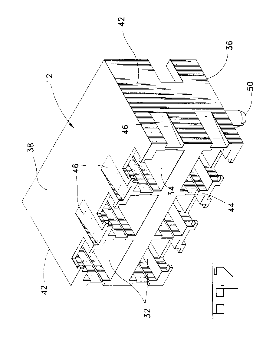
connector grounding tab 30 in greater detail, it may be helpful to generally review thedielectric connector housing 12 and stamped and formedmetal shielding member 14 of Figures 5 and 6-8, respectively. Considering first theconnector housing 12, it typically is molded from a plastic compound, such as a high temperature polyester, and comprises one ormore cavities 32 for electrically engaging complementary modular plugs, as known in the art. Thecavities 32, for a multi port connector, are typically arranged in side-by-side fashion in two rows separated by adielectric wall 34. Structurally, theconnector housing 12 comprises a board engaginglower surface 36, atop surface 38, a pair ofside walls 42, and a front ormating face 44. A unique feature of thehousing 12 is the provision of theplural recesses 46, angled forwardly from the interior oftop surface 38,lower surface 36, andside walls 42, toward the front ormating face 44. With regard to therecesses 46 aicng the top and bottom, it will be noted that such recesses are preferably arranged betweenadjacent cavities 32. Finally, thehousing 12 includes a pair ofboard mounting posts 50, as known in the art. - The
metal shielding member 14 is a one-piece metal shell stamped and formed from a sheet metal blank. The shell, illustrated in the formed condition in Figure 6, includes afront face 52, havingconnector receiving openings 54, corresponding in number and arrangement to thecavities 32 of thehousing 12. Each such opening 54 is provided with a pair oftabs 56 which are arranged to be bent inwardly toward the cavity walls. Theshield member 14 further includes atop wall 58, a pair ofside walls 60, a partial bottom wall 62 (see Figure 8) and a pivotal or hingedrear wall 64. While the top, sides and rear walls fully cover or shield the connector housing 12, the lower orbottom wall 62 covers only the forward portion of the housing. It will be recalled, particularly from Figures 1 and 2, that solder posts orpins 15 extend from theconnector 10, although not shown in Figure 8, for engagement with complementary through holes in thePCB 16, as known in the art. Additionally, thebottom wall 62 includes a pair of side recesses or cut-outs 63 to accommodate themounting posts 50. Finally, extending from the lower edge ofside walls 60 aresolder tabs 65 for grounding to appropriate grounding traces in thePCB 16. Though the manner of forming theshield member 14 is not illustrated by initially depicting a flat blank, it will be understood from the above description and drawings that thefront face 52 is essentially the center of the flat blank, with therespective side walls 60,top wall 58 andbottom wall 62 formed therefrom. Therear wall 64, most clearly illustrated in Figure 9, is bent and formed along therear edge 74 oftop wall 58. - A characteristic feature of the top wall, side walls, and bottom wall, is the provision of plural, cantilevered
ground tabs 30, where such tabs extend from aninterior position 66 toward thefront face 52, betweenparallel slots 68. Thetabs 30, as more clearly illustrated in Figures 3 and 4, at thefree end 70 thereof, include a reversely formedend 72. By this arrangement, stubbing of theend 70 is prevented during loading of the connector into the opening ofpanel 26. Additionally, breakage or overstressing is avoided upon removal of the connector therefrom. Overstressing is further avoided by the provision of a long moment arm, i.e. from theinterior position 66 to thefront face 52. Finally, grounding contact with themetal panel 26 is assured by the fact that the tab formedend 72 extends above the plane of the respective walls, i.e.top wall 58,side walls 60,lower wall 62, in the resiled or relaxed position illustrated in Figure 3. As best seen in Figure 4, when the connector is loaded into the opening panel of 26 thetabs 30 are flexed inwardly toward theirrespective recesses 46, with the reversely formedend 72 in grounding contact with themetal panel 26. - To function as an effective shield, the shielding
member 14 must encompass and lie contiguous with theunderlying connector housing 12. Therear wall 64 is hingedly mounted from therear edge 74 oftop wall 58 to allow access into the formed shieldingmember 14, note the loading sequence of Figures 9 and 10. After loading, therear wall 64 is closed in latching engagement with the rear of theside walls 60. This may be accomplished by providing aflanged portion 76 along the side edges of the rear wall, where theflanged portion 76 may include a pair ofwindows 78, andcomplementary lances 80 along therear edges 82 of theside walls 60. The rear portion of theside walls 60 may include a steppedportion 84, which includes thelances 80, so that when therear wall 64 is hingedly moved into latching engagement with theside walls 60, the sides of the assembly will be flush, that is, theflanged portions 76 will seat within the steppedportions 84. - The rear loading sequence is illustrated in Figures 9 and 10. After forming of the
ground shield member 14 in the manner described above, the hingedrear wall 64 and thetop wall 58 remain raised in the manner shown in Figure 9. In this position, theconnector housing 12 is inserted within the formed shield, note the direction arrow, and as shown in Figure 10, therear wall 64 is pivoted into contact with therespective side walls 60, while thetop wall 58 comes into contact with thetop surface 38 of theconnector housing 12. As therear wall 64 engages saidwalls 60, thelances 80 snap intowindows 78 to thereby secure the shield into position. - Figures 11 and 12, sectional views similar to Figures 3 and 4, respectively, illustrate an alternate shape to the cantilevered ground tabs 30'. In this embodiment, the peak or reverse
bend portion 90 has been flattened to provide grounding contact over a broader surface. This may be particularly beneficial to ensure registration with themetal panel 92, which may vary in thickness from one application to another.
Claims (8)
- A shielded high performance electrical connector of the type for mounting to a printed circuit board, and adapted to be secured within a metal panel housing, where said connector comprises a dielectric housing (12) having a planar top surface (38), a printed circuit board engaging surface (36), a pair of side walls (42), a rear wall and a front surface (44), and at least one cavity (32) extending interiorly from the front surface thereof for electrically engaging a complementary electrical connector, said connector including a one-piece shielding member (14) stamped and formed from a sheet metal blank to offer low resistance grounding of the connector to said metal panel housing, said shielding member (14) having substantially planar top and side walls (58, 60) adapted to lie contiguous with said top surface (38) and said side walls (42), respectively, said connector being characterized by:
a plurality of elongated cantilevered tabs (30) struck from said top and side walls (58, 60), each of said tabs having a secured end (66) and a free end (70), wherein said secured end extends from an internal location remote from said front surface, said free end extends toward said front surface, and said free end has a reverse bend (72) which in a resiled position extends outwardly of the plane of the wall (58, 60) from which it is struck. - The shielded electrical connector according to claim 1, wherein said shielding member includes a shielding face (52) which overlies said front surface (44), and that said shielding face includes a complementary opening (54) aligned with a respective said cavity (32).
- The shielded electrical connector according to claim 1, wherein said shielding member includes a rear wall (64) which is hingedly secured to said top wall (58) for overlying said rear wall of said dielectric housing.
- The shielded electrical connector according to claim 3, wherein said rear wall (64) includes a flanged portion (76) to engage a rear edge portion (82) of one of the side walls (60).
- The shielded electrical connector according to claim 1, wherein said dielectric housing includes a recess (46) extending from said front surface (44) in registration with each said tab (30) to allow inward deflection of said tab when secured within a metal panel housing.
- The shielded electrical connector according to claim 1, wherein said dielectric housing comprises an array of said cavities (32) in side-by-side relationship, and that said tabs (30) along the top surface are aligned between adjacent said cavities.
- The shielded electrical connector according to claim 5, wherein the end most portion of each said free end (70) is directed toward its respective said recess (46).
- The shielded electrical connector according to claim 1, wherein each said tab (30) is defined by a pair of parallel slots (68) extending inwardly from said front surface.
Applications Claiming Priority (2)
| Application Number | Priority Date | Filing Date | Title |
|---|---|---|---|
| US403028 | 1995-03-13 | ||
| US08/403,028 US5496195A (en) | 1995-03-13 | 1995-03-13 | High performance shielded connector |
Publications (2)
| Publication Number | Publication Date |
|---|---|
| EP0732776A1 true EP0732776A1 (en) | 1996-09-18 |
| EP0732776B1 EP0732776B1 (en) | 1998-09-16 |
Family
ID=23594221
Family Applications (1)
| Application Number | Title | Priority Date | Filing Date |
|---|---|---|---|
| EP96301094A Expired - Lifetime EP0732776B1 (en) | 1995-03-13 | 1996-02-19 | High performance shielded connector |
Country Status (5)
| Country | Link |
|---|---|
| US (1) | US5496195A (en) |
| EP (1) | EP0732776B1 (en) |
| JP (1) | JP3769705B2 (en) |
| BR (1) | BR9600963A (en) |
| DE (1) | DE69600647T2 (en) |
Cited By (2)
| Publication number | Priority date | Publication date | Assignee | Title |
|---|---|---|---|---|
| EP1209775A2 (en) * | 2000-11-28 | 2002-05-29 | J.S.T. Mfg. Co., Ltd. | Modular jack |
| SG101427A1 (en) * | 1999-08-10 | 2004-01-30 | Molex Inc | Case of electronic connector |
Families Citing this family (47)
| Publication number | Priority date | Publication date | Assignee | Title |
|---|---|---|---|---|
| US5637015A (en) * | 1995-08-31 | 1997-06-10 | Hon Hai Precision Ind. Co., Ltd. | Shielded electrical connector |
| USD378510S (en) * | 1995-12-08 | 1997-03-18 | Hon Hai Precision Ind. Co., Ltd. | Dual connector |
| US5696669A (en) * | 1996-01-11 | 1997-12-09 | Molex Incorporated | Shielding system for PC cards |
| US5639267A (en) * | 1996-01-26 | 1997-06-17 | Maxconn Incorporated | Modular jack assembly |
| US5685739A (en) * | 1996-02-14 | 1997-11-11 | The Whitaker Corporation | Shielded electrical connector |
| US5733146A (en) * | 1996-04-01 | 1998-03-31 | Block; Dale A. | Shield for modular electrical connector |
| US5766041A (en) * | 1996-05-31 | 1998-06-16 | The Whitaker Corporation | Shield member for panel mount connector |
| US5738544A (en) * | 1996-06-27 | 1998-04-14 | The Whitaker Corporation | Shielded electrical connector |
| US5755595A (en) * | 1996-06-27 | 1998-05-26 | Whitaker Corporation | Shielded electrical connector |
| US5676569A (en) * | 1996-07-25 | 1997-10-14 | The Whitaker Corporation | Holder for several electrical connectors |
| US5788538A (en) * | 1996-07-31 | 1998-08-04 | Berg Technology, Inc. | Shield for modular jack |
| US5775946A (en) * | 1996-08-23 | 1998-07-07 | Amphenol Corporation | Shielded multi-port connector and method of assembly |
| JP3070003B2 (en) * | 1996-09-06 | 2000-07-24 | タイコエレクトロニクスアンプ株式会社 | Shield type connector and manufacturing method thereof |
| US6077120A (en) * | 1996-09-06 | 2000-06-20 | The Whitaker Corporation | Shielded connector of interfitting C-shaped shield members on a housing and method for manufacturing the same |
| EP0844700A1 (en) * | 1996-11-26 | 1998-05-27 | Koninklijke Philips Electronics N.V. | Multiple outlet for electronic equipment |
| US6454603B2 (en) * | 1997-03-07 | 2002-09-24 | Berg Technology, Inc. | Shielded connector with integral latching and ground structure |
| US5865646A (en) * | 1997-03-07 | 1999-02-02 | Berg Technology, Inc. | Connector shield with integral latching and ground structure |
| US6068520A (en) | 1997-03-13 | 2000-05-30 | Berg Technology, Inc. | Low profile double deck connector with improved cross talk isolation |
| US5885100A (en) * | 1997-05-12 | 1999-03-23 | Molex Incorporated | Electrical connector with light transmission means |
| US5934940A (en) * | 1997-07-23 | 1999-08-10 | Molex Incorporated | Shielded electrical connector |
| US5961350A (en) * | 1997-07-31 | 1999-10-05 | The Whitaker Corporation | Modular side-by-side connectors |
| US6000955A (en) | 1997-12-10 | 1999-12-14 | Gabriel Technologies, Inc. | Multiple terminal edge connector |
| US6162089A (en) * | 1997-12-30 | 2000-12-19 | The Whitaker Corporation | Stacked LAN connector |
| US6709280B1 (en) * | 2002-01-17 | 2004-03-23 | Arlington Industries, Inc. | Fitting with improved continuity |
| US6036547A (en) * | 1998-03-05 | 2000-03-14 | Berg Technology, Inc. | Double deck gang jack exhibiting suppressed mutual crosstalk |
| US6142828A (en) * | 1998-11-24 | 2000-11-07 | The Whitaker Corporation | Shielded connector having adjustable cable exit |
| TW395583U (en) * | 1998-12-28 | 2000-06-21 | Hon Hai Prec Ind Co Ltd | Electronic card connector assembly |
| EP1045484A1 (en) * | 1999-04-09 | 2000-10-18 | Molex Incorporated | Shielded electrical connector |
| US6116924A (en) * | 1999-05-25 | 2000-09-12 | 3Com Corporation | Electromagnetic emissions shielding structure for circuit board connector assembly |
| NL1012694C2 (en) * | 1999-07-23 | 2001-01-24 | Berg Electronics Mfg | Connector and plug or socket for use therein. |
| US7942888B2 (en) * | 1999-09-13 | 2011-05-17 | Rex Medical, L.P. | Vascular hole closure device |
| US6537084B2 (en) | 1999-09-30 | 2003-03-25 | Berg Technology, Inc. | Electrical connector with electrical shield having latch and mounting arms |
| US6390851B1 (en) | 1999-10-16 | 2002-05-21 | Berg Technology, Inc. | Electrical connector with internal shield |
| US6325672B1 (en) | 1999-10-16 | 2001-12-04 | Berg Technology, Inc. | Electrical connector with internal shield and filter |
| US6585540B2 (en) * | 2000-12-06 | 2003-07-01 | Pulse Engineering | Shielded microelectronic connector assembly and method of manufacturing |
| US7232340B2 (en) | 2004-02-20 | 2007-06-19 | Adc Incorporated | Methods and systems for minimizing alien crosstalk between connectors |
| US7241181B2 (en) | 2004-06-29 | 2007-07-10 | Pulse Engineering, Inc. | Universal connector assembly and method of manufacturing |
| US7351105B2 (en) * | 2005-11-09 | 2008-04-01 | Molex Incorporated | Board mounted shielded electrical connector |
| US7294024B2 (en) | 2006-01-06 | 2007-11-13 | Adc Telecommunications, Inc. | Methods and systems for minimizing alien crosstalk between connectors |
| JP4175657B2 (en) * | 2006-01-17 | 2008-11-05 | 日本航空電子工業株式会社 | connector |
| JP4775116B2 (en) * | 2006-05-30 | 2011-09-21 | 横河電機株式会社 | Connector attachment |
| WO2011032205A1 (en) * | 2009-09-16 | 2011-03-24 | Power & Data Corporation Pty Ltd | Methods, systems and devices for facilitating data access |
| WO2011056979A2 (en) * | 2009-11-06 | 2011-05-12 | Molex Incorporated | Modular jack with enhanced shielding |
| JP2014035946A (en) | 2012-08-09 | 2014-02-24 | Yazaki Corp | On-board shield connector |
| US9601857B2 (en) | 2013-05-23 | 2017-03-21 | Pulse Electronics, Inc. | Methods and apparatus for terminating wire wound electronic devices |
| US9716344B2 (en) | 2013-07-02 | 2017-07-25 | Pulse Electronics, Inc. | Apparatus for terminating wire wound electronic components to an insert header assembly |
| US9401561B2 (en) | 2013-07-02 | 2016-07-26 | Pulse Electronics, Inc. | Methods and apparatus for terminating wire wound electronic components to a header assembly |
Citations (5)
| Publication number | Priority date | Publication date | Assignee | Title |
|---|---|---|---|---|
| CH660934A5 (en) * | 1983-02-28 | 1987-05-29 | Feller Ag | Screening casing and an electrical plug assembly equipped therewith, especially an apparatus plug with an interference-protection filter |
| US5013262A (en) * | 1989-06-26 | 1991-05-07 | Hosiden Electronics Co., Ltd. | Multi-contact socket |
| US5083945A (en) * | 1991-02-01 | 1992-01-28 | Molex Incorporated | Shielded electrical connector assembly |
| EP0524426A1 (en) * | 1991-06-21 | 1993-01-27 | The Whitaker Corporation | Electrical connector |
| US5254010A (en) * | 1992-09-16 | 1993-10-19 | Amp Incorporated | Securing a surface mount electrical connector in a metal shielding shell |
Family Cites Families (4)
| Publication number | Priority date | Publication date | Assignee | Title |
|---|---|---|---|---|
| US4659163A (en) * | 1984-06-13 | 1987-04-21 | Amp Incorporated | Filtered shielded connector assembly |
| FR2652229B1 (en) * | 1989-09-19 | 1991-11-15 | Bull Sa | SHIELDING ASSEMBLY FOR A COLLECTOR BLOCK CONNECTED TO ELECTRICAL EQUIPMENT PLACED INSIDE A CHASSIS. |
| US5378172A (en) * | 1994-03-10 | 1995-01-03 | Molex Incorporated | Low profile shielded jack |
| US5387130A (en) * | 1994-03-29 | 1995-02-07 | The Whitaker Corporation | Shielded electrical cable assembly with shielding back shell |
-
1995
- 1995-03-13 US US08/403,028 patent/US5496195A/en not_active Expired - Lifetime
-
1996
- 1996-02-19 DE DE69600647T patent/DE69600647T2/en not_active Expired - Lifetime
- 1996-02-19 EP EP96301094A patent/EP0732776B1/en not_active Expired - Lifetime
- 1996-03-08 BR BR9600963A patent/BR9600963A/en not_active IP Right Cessation
- 1996-03-11 JP JP08314796A patent/JP3769705B2/en not_active Expired - Lifetime
Patent Citations (5)
| Publication number | Priority date | Publication date | Assignee | Title |
|---|---|---|---|---|
| CH660934A5 (en) * | 1983-02-28 | 1987-05-29 | Feller Ag | Screening casing and an electrical plug assembly equipped therewith, especially an apparatus plug with an interference-protection filter |
| US5013262A (en) * | 1989-06-26 | 1991-05-07 | Hosiden Electronics Co., Ltd. | Multi-contact socket |
| US5083945A (en) * | 1991-02-01 | 1992-01-28 | Molex Incorporated | Shielded electrical connector assembly |
| EP0524426A1 (en) * | 1991-06-21 | 1993-01-27 | The Whitaker Corporation | Electrical connector |
| US5254010A (en) * | 1992-09-16 | 1993-10-19 | Amp Incorporated | Securing a surface mount electrical connector in a metal shielding shell |
Cited By (3)
| Publication number | Priority date | Publication date | Assignee | Title |
|---|---|---|---|---|
| SG101427A1 (en) * | 1999-08-10 | 2004-01-30 | Molex Inc | Case of electronic connector |
| EP1209775A2 (en) * | 2000-11-28 | 2002-05-29 | J.S.T. Mfg. Co., Ltd. | Modular jack |
| EP1209775A3 (en) * | 2000-11-28 | 2005-04-20 | J.S.T. Mfg. Co., Ltd. | Modular jack |
Also Published As
| Publication number | Publication date |
|---|---|
| BR9600963A (en) | 1997-12-30 |
| DE69600647D1 (en) | 1998-10-22 |
| JPH08255657A (en) | 1996-10-01 |
| JP3769705B2 (en) | 2006-04-26 |
| EP0732776B1 (en) | 1998-09-16 |
| US5496195A (en) | 1996-03-05 |
| DE69600647T2 (en) | 1999-04-08 |
Similar Documents
| Publication | Publication Date | Title |
|---|---|---|
| US5496195A (en) | High performance shielded connector | |
| US6319061B1 (en) | Pair of shielded electrical connectors with a grounding element therebetween | |
| US5934940A (en) | Shielded electrical connector | |
| EP0658953B1 (en) | Multi-port modular jack assembly | |
| US4679879A (en) | Plug and receptacle connector assembly | |
| US6083046A (en) | Receptacle connector | |
| US5775946A (en) | Shielded multi-port connector and method of assembly | |
| US5601451A (en) | Combination connector | |
| EP1356549B1 (en) | Connector interface and retention system for high-density connector | |
| US6053773A (en) | Electrical input/output connector | |
| US6120318A (en) | Stacked electrical connector having visual indicator subassembly | |
| US7192297B1 (en) | Cable connector assembly with improved shell | |
| US7086901B2 (en) | Shielded electrical connector | |
| EP0994535B1 (en) | Modular connector with reduced crosstalk | |
| JPH0629060A (en) | Shielded connector | |
| EP2224547A1 (en) | Shielded cassette for a cable interconnect system | |
| JPH02195675A (en) | Low profile shield jack | |
| US20040180577A1 (en) | Shielded electrical connector | |
| CA2144704A1 (en) | Combination connector | |
| US20040259421A1 (en) | Cable connector assembly having improved shield members | |
| US5695362A (en) | Hybrid grounded and stacked connector assembly with audio jacks | |
| KR19980087500A (en) | Shielded electrical connectors | |
| US7086888B2 (en) | Serial ATA cable assembly with small size | |
| US7052329B2 (en) | Electrical connector with an internal modem | |
| US6165008A (en) | Electrical connector for flexible flat cable |
Legal Events
| Date | Code | Title | Description |
|---|---|---|---|
| PUAI | Public reference made under article 153(3) epc to a published international application that has entered the european phase |
Free format text: ORIGINAL CODE: 0009012 |
|
| AK | Designated contracting states |
Kind code of ref document: A1 Designated state(s): DE FR GB IT NL SE |
|
| 17P | Request for examination filed |
Effective date: 19961021 |
|
| 17Q | First examination report despatched |
Effective date: 19970122 |
|
| GRAG | Despatch of communication of intention to grant |
Free format text: ORIGINAL CODE: EPIDOS AGRA |
|
| GRAG | Despatch of communication of intention to grant |
Free format text: ORIGINAL CODE: EPIDOS AGRA |
|
| GRAH | Despatch of communication of intention to grant a patent |
Free format text: ORIGINAL CODE: EPIDOS IGRA |
|
| GRAH | Despatch of communication of intention to grant a patent |
Free format text: ORIGINAL CODE: EPIDOS IGRA |
|
| GRAA | (expected) grant |
Free format text: ORIGINAL CODE: 0009210 |
|
| AK | Designated contracting states |
Kind code of ref document: B1 Designated state(s): DE FR GB |
|
| RBV | Designated contracting states (corrected) |
Designated state(s): DE FR GB |
|
| REF | Corresponds to: |
Ref document number: 69600647 Country of ref document: DE Date of ref document: 19981022 |
|
| ET | Fr: translation filed | ||
| NLXE | Nl: other communications concerning ep-patents (part 3 heading xe) |
Free format text: PAT. BUL. 11/98 SHOULD BE DELETED |
|
| PLBE | No opposition filed within time limit |
Free format text: ORIGINAL CODE: 0009261 |
|
| STAA | Information on the status of an ep patent application or granted ep patent |
Free format text: STATUS: NO OPPOSITION FILED WITHIN TIME LIMIT |
|
| 26N | No opposition filed | ||
| REG | Reference to a national code |
Ref country code: GB Ref legal event code: IF02 |
|
| REG | Reference to a national code |
Ref country code: FR Ref legal event code: PLFP Year of fee payment: 20 |
|
| PGFP | Annual fee paid to national office [announced via postgrant information from national office to epo] |
Ref country code: DE Payment date: 20150226 Year of fee payment: 20 |
|
| PGFP | Annual fee paid to national office [announced via postgrant information from national office to epo] |
Ref country code: GB Payment date: 20150226 Year of fee payment: 20 Ref country code: FR Payment date: 20150217 Year of fee payment: 20 |
|
| REG | Reference to a national code |
Ref country code: DE Ref legal event code: R071 Ref document number: 69600647 Country of ref document: DE |
|
| REG | Reference to a national code |
Ref country code: GB Ref legal event code: PE20 Expiry date: 20160218 |
|
| PG25 | Lapsed in a contracting state [announced via postgrant information from national office to epo] |
Ref country code: GB Free format text: LAPSE BECAUSE OF EXPIRATION OF PROTECTION Effective date: 20160218 |