EP0729840A1 - Ic for driving printer and print head - Google Patents
Ic for driving printer and print head Download PDFInfo
- Publication number
- EP0729840A1 EP0729840A1 EP95932956A EP95932956A EP0729840A1 EP 0729840 A1 EP0729840 A1 EP 0729840A1 EP 95932956 A EP95932956 A EP 95932956A EP 95932956 A EP95932956 A EP 95932956A EP 0729840 A1 EP0729840 A1 EP 0729840A1
- Authority
- EP
- European Patent Office
- Prior art keywords
- drive
- pads
- edge
- section
- longitudinal edge
- Prior art date
- Legal status (The legal status is an assumption and is not a legal conclusion. Google has not performed a legal analysis and makes no representation as to the accuracy of the status listed.)
- Granted
Links
Images


Classifications
-
- B—PERFORMING OPERATIONS; TRANSPORTING
- B41—PRINTING; LINING MACHINES; TYPEWRITERS; STAMPS
- B41J—TYPEWRITERS; SELECTIVE PRINTING MECHANISMS, i.e. MECHANISMS PRINTING OTHERWISE THAN FROM A FORME; CORRECTION OF TYPOGRAPHICAL ERRORS
- B41J2/00—Typewriters or selective printing mechanisms characterised by the printing or marking process for which they are designed
- B41J2/315—Typewriters or selective printing mechanisms characterised by the printing or marking process for which they are designed characterised by selective application of heat to a heat sensitive printing or impression-transfer material
- B41J2/32—Typewriters or selective printing mechanisms characterised by the printing or marking process for which they are designed characterised by selective application of heat to a heat sensitive printing or impression-transfer material using thermal heads
- B41J2/35—Typewriters or selective printing mechanisms characterised by the printing or marking process for which they are designed characterised by selective application of heat to a heat sensitive printing or impression-transfer material using thermal heads providing current or voltage to the thermal head
- B41J2/355—Control circuits for heating-element selection
-
- B—PERFORMING OPERATIONS; TRANSPORTING
- B41—PRINTING; LINING MACHINES; TYPEWRITERS; STAMPS
- B41J—TYPEWRITERS; SELECTIVE PRINTING MECHANISMS, i.e. MECHANISMS PRINTING OTHERWISE THAN FROM A FORME; CORRECTION OF TYPOGRAPHICAL ERRORS
- B41J2/00—Typewriters or selective printing mechanisms characterised by the printing or marking process for which they are designed
- B41J2/315—Typewriters or selective printing mechanisms characterised by the printing or marking process for which they are designed characterised by selective application of heat to a heat sensitive printing or impression-transfer material
- B41J2/32—Typewriters or selective printing mechanisms characterised by the printing or marking process for which they are designed characterised by selective application of heat to a heat sensitive printing or impression-transfer material using thermal heads
- B41J2/345—Typewriters or selective printing mechanisms characterised by the printing or marking process for which they are designed characterised by selective application of heat to a heat sensitive printing or impression-transfer material using thermal heads characterised by the arrangement of resistors or conductors
Definitions
- the present invention relates to a drive IC for driving a recording element, such as a heating element, of a printhead which is used as a recording device for a facsimile machine, other office automation machine or the like.
- the present invention also relates to a printhead using such a drive IC.
- Fig. 7 shows a structure of a thermal head as an example of a printhead which is used as a recording device for a facsimile machine, other office automation machine or the like, wherein a heating resistor is selectively heated to thermally cause a thermosensitive paper, which is fed in contact with the thermal head, to make a change in color for recording.
- a printhead substrate 51 made of alumina ceramic for example is formed with a linear heating resistor 52, a common electrode 53 including comb-like teeth each having a tip in contact with the heating resistor 52, and a multiplicity of individual electrodes 54 each having one end in contact with the heating resistor 52 between adjacent teeth of the common electrode 53.
- the printhead substrate 51 carries a plurality of drive ICs 55 attached thereon by die bonding.
- the drive ICs 55 are wire-bonded to the individual electrodes 54 each at the other end thereof while also wire-bonded to a multiplicity of conductive connecting portions 57 formed on a printed circuit board 56.
- a conventional drive IC 55 for driving a recording element, such as a heating resistor 52, of a printer is generally rectangular as viewed from above, and has a pair of longitudinal edges 55a, 55b.
- a multiplicity of output pads 61 are disposed in a staggered arrangement along one of the paired longitudinal edges 5a, 5b, that is, the longitudinal edge 55a (hereinafter referred to as "first longitudinal edge") which is closer to the heating resistor 52.
- first longitudinal edge the longitudinal edge 55a
- the drive IC 55 is provided with a multiplicity of signal pads 62 and power pads 63 which are arranged along the other longitudinal edge, that is, the longitudinal edge 55b (hereinafter referred to as "second longitudinal edge") which is closer to the printed circuit board 56.
- the signal pads 62 and the power pads 63 are wire-bonded to the connecting portions 57.
- the drive IC 55 has a drive section 64 and a signal processing section 65 disposed between the output pads 61 and the signal pads 62 or the power pads 63.
- the drive section 64 is closer to the first longitudinal edge 55a than the signal processing section 65.
- the drive section 64 is connected to the output pads 61 via wirings and includes a circuit for turning on and off an electrical current passing through the portions of the heating resistor 52 located between the individual electrodes 54 and the teeth of the common electrode 53.
- the signal processing section 65 is connected to the signal pads 62 by wirings and includes logic circuits as well as a shift register for controlling the drive section 64 by processing the signals which are fed externally via the connecting portions 57.
- the drive IC 55 is die-bonded to the printhead substrate 51 in a manner such that the second longitudinal edge 55b of the drive IC 55 positionally deviates slightly inward from an edge of the printhead substrate 51, thereby ensuring that the signal pads 62 and the power pads 63 are located above the flat portion of the upper surface of the printhead substrate 51.
- a respective printhead substrate 51 is obtained by dividing a master substrate formed with multiple printhead substrates 51 along cutting lines, corners of the above-mentioned edge of the printhead substrate may be often damaged during the dividing process, thereby failing to make the upper surface of the printhead substrates 51 to be a complete plane due to the presence of a chipped portion extending for a certain width from the edge.
- the drive IC 55 is die-bonded onto the printhead substrate 51 in a manner such that the second longitudinal edge 55b of the drive IC 55 positionally corresponds to the edge of the printhead substrate 51, the lower surface of the drive IC 55 is to face the incomplete plane of the upper surface of the printhead substrate 51.
- the drive IC 55 may be damaged or come off from the printhead substrate 51 due to a shock caused by the wire-bonding at the signal pads 62 and the power pads 63. It is for prevention of such problems that the second longitudinal edge 55b of the drive IC 55 is arranged to positionally deviate inwardly from the edge of the printed substrate 51 by a predetermined amount. Further, when the second longitudinal edge 55b of the drive IC 55 is arranged to positionally deviate inwardly from the edge of the printhead substrate 51, setting the amount of deviation at a rather larger value can make it unnecessary to strictly require accurate positioning of the die-bonding for the drive IC 55, thereby facilitating the die-bonding process.
- an object of the present invention is to provide a printer drive IC which, without suffering any problems such as a damage or coming off during the wire-bonding process at signal pads and power pads, enables reduction in size of a printhead substrate.
- Another object of the present invention is to provide a printhead wherein a printhead substrate and a printed circuit board can be firmly attached to each other by hard coat when the printer drive ICs are arranged to deviate outwardly from an edge of the printhead substrate.
- a drive IC for driving a recording element of a printer, the drive IC being generally quadrilateral as viewed from above, the drive IC comprising a first edge which is directed toward the recording element of the printer and a second edge opposite to the first edge, the drive IC further comprising in the successive order from the first edge toward the second edge: a region for arranging output pads; a region for arranging a drive section for driving the recording element of the printer; and a region for arranging a signal processing section which includes a logic circuit section and a register section to process input signals for output to the drive section; wherein the drive IC also comprises signal pads and power pads which are arranged closer to the first edge than the region for arranging the logic circuit section of the signal processing section.
- the signal pads and the power pads are arranged closer to the first edge than the region for arranging the logic circuit section of the signal processing section, the signal pads and the power pads are to be disposed above a flat portion which is located inwardly from a damaged portionaat an edge of the upper surface of the printhead substrate even when the second edge of the drive IC is arranged to positionally correspond to the above-mentioned edge of the printhead substrate or arranged to project slightly outward from the same edge thereof.
- the drive IC can be prevented from suffering a damage or coming off from the printhead substrate during the wire bonding at the signal pads and the power pads.
- a drive IC for driving a recording element of a printer, the drive IC being generally quadrilateral as viewed from above, the drive IC comprising a first edge which is directed toward the recording element of the printer and a second edge opposite to the first edge, the drive IC further comprising: output pads arranged along the first edge; and signal pads and power pads which are spaced from the second edge by no less than 150 ⁇ m.
- the signal pads and the power pads are spaced from the second edge by no less than 150 ⁇ m, the signal pads and the power pads are to be disposed above a flat portion which is located inwardly from a damaged portion at an edge of the upper surface of the printhead substrate even when the second edge of the drive IC is arranged to positionally correspond to the above-mentioned edge of the printhead substrate or arranged to project slightly outward from the same edge thereof.
- the drive IC can be prevented from suffering a damage or coming off from the printhead substrate during the wire bonding at the signal pads and the power pads.
- the damaged portion at the above-mentioned edge of the upper surface of the printhead substrate extend only for a width of no more than 150 ⁇ m from the same edge thereof. Therefore, by arranging the signal pads and the power pads to be spaced from the second edge of the drive IC by no less than 150 ⁇ m, the signal pads and the power pads can be prevented from being located above the damaged portion of the upper surface of the printhead substrate even when the second edge of the drive IC is arranged to positionally correspond to the above-mentioned edge of the printhead substrate or arranged to project slightly outward from the same edge thereof. Further, since the width of the logic circuit section of the signal processing section of the drive IC is approximately 150 ⁇ m, it is possible to dispose the logic circuit section of the signal processing section between the signal and power pads and the second edge of the drive IC.
- a drive IC for driving a recording element of a printer, the drive IC being generally rectangular as viewed from above, the drive IC comprising a first longitudinal edge which is directed toward the recording element of the printer and a second longitudinal edge opposite to the first longitudinal edge, the drive IC further comprising in the successive order from the first longitudinal edge toward the second longitudinal edge: a plurality of output pads; a drive section which includes drive circuits connected to the output pads for driving the recording element of the printer; and a signal processing section which includes a logic circuit section for processing input signals and controlling the drive section, the logic circuit section including logic circuits; wherein the drive IC also comprises a plurality of signal pads connected to the signal processing section for receiving input signals, and a plurality of power pads connected to the signal processing section and the drive section for input of power supply, the signal pads and the power pads being arranged closer to the first longitudinal edge than the logic circuit section of the signal processing section.
- the signal pads and the power pads are arranged closer to the first longitudinal edge than the logic circuit section of the signal processing section, the signal pads and the power pads are to be disposed above a flat portion which is located inwardly from a damaged portion at an edge of the upper surface of the printhead substrate even when the second edge of the drive IC is arranged to positionally correspond to the above-mentioned edge of the upper surface of the printhead substrate or arranged to project slightly outward from the same edge thereof.
- the drive IC can be prevented from suffering a damage or coming off from the printhead substrate during the wire bonding at the signal pads and the power pads.
- the logic circuit section of the signal processing section is arranged closer to the second longitudinal edge than the signal pads and the power pads, the shorter edges of the drive IC can be prevented from becoming large in dimension.
- At least either of the signal pads and the power pads is disposed between the signal processing section and the drive section.
- At least either of the signal pads and the power pads is disposed between the drive section and the output pads.
- the signal processing section includes a logic circuit section and a register section which is provided with a shift register and a latch circuit for processing input signals and controlling the drive section, wherein the register section is arranged closer to the first longitudinal edge than the logic circuit section, and the signal pads and the power pads are disposed between the logic circuit section and the register section.
- the signal pads and/or the power pads are arranged closer to the first longitudinal edge than the logic circuit section of the signal processing section and along either or both of the shorter edges.
- a drive IC for driving a recording element of a printer, the drive IC being generally rectangular as viewed from above, the drive IC comprising a first longitudinal edge which is closer to the recording element of the printer and a second longitudinal edge opposite to the first longitudinal edge, the drive IC further comprising: a plurality of output pads arranged along the first longitudinal edge; wherein a plurality of signal pads connected to a signal processing section for receiving input signals as well as a plurality of power pads connected to the signal processing section and a drive section for input of power supply are spaced from the second longitudinal edge by no less than 150 ⁇ m.
- the signal pads and the power pads may be spaced from the second longitudinal edge by no less than 250 ⁇ m.
- the width of the signal processing section of the drive IC is approximately 250 ⁇ m, the signal processing section can be disposed between the signal and power pads and the second longitudinal edge of the drive IC.
- the signal pads and the power pads may be spaced from the second longitudinal edge by no less than 600 ⁇ m.
- the signal processing section of the drive IC has a width of approximately 250 ⁇ m and the drive section has a width of approximately 350 ⁇ m, both of the signal processing section and the drive section can be disposed between the signal and power pads and the second longitudinal edge of the drive IC.
- a printhead comprising: a printhead substrate which is generally rectangular as viewed from above, the substrate including a recording element and a drive IC for driving the recording element; and a printed circuit board for supplying signals and power to the drive IC; wherein the drive IC is generally quadrilateral as viewed from above, the drive IC having a first edge which is closer to the recording element and a second edge opposite to the first edge, the drive IC further having output pads, signal pads and power pads, the output pads being arranged along the first edge, the signal pads and the power pads being spaced from the second edge by no less than 150 ⁇ m ; wherein the printed circuit board and the printhead substrate are arranged in a manner such that an edge of the printhead substrate and an edge of the printed circuit board face each other with a predetermined spacing; and wherein the second edge of the drive IC protrudes from said edge of the printhead substrate by a predetermined amount.
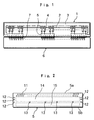
- Fig. 1 is a schematic plan view showing a printhead provided with printer drive ICs embodying the present invention.
- a printhead substrate 1 made of alumina ceramic for example is formed with a linear heating resistor 2, a common electrode 3 including comb-like teeth each having a tip in contact with the heating resistor 2, and a multiplicity of individual electrodes 4 each having one end in contact with the heating resistor 2 between adjacent teeth of the common electrode 3.
- the printhead substrate 1 is provided with a plurality of drive ICs 5 fixed thereon by die bonding.
- the drive ICs 5 are wire-bonded to the individual electrodes 4 each at the other end thereof while also wire-bonded to a plurality of conductive connecting terminals 7 which are formed on a printed circuit board 6.
- Fig. 2 is a schematic plan view illustrating a pad arrangement of each printer drive IC embodying the present invention.
- the drive IC 5 is generally rectangular as viewed from above, and has a pair of longitudinal edges 5a, 5b.
- a plurality of output pads 11 are disposed in a staggered arrangement along one of the paired longitudinal edges 5a, 5b, that is, the longitudinal edge 5a (hereinafter referred to as "first longitudinal edge") which is closer to the heating resistor 2.
- first longitudinal edge the longitudinal edge 5a
- Each of the output pads 11 is wire-bonded to said other end of a respective individual electrode 4.
- the drive IC 5 is provided with a plurality of signal pads 12 which are arranged along the shorter edges and spaced from the other longitudinal edge 5b (hereinafter referred to as "second longitudinal edge") by at least 150 ⁇ m.
- the drive IC 5 is also provided with a plurality of power pads 13 which are arranged in parallel to the second longitudinal edge 5b and spaced therefrom by at least 150 ⁇ m.
- the signal pads 12 and the power pads 13 are wire-bonded to the connecting terminals 7 on the printed circuit board 6.
- the drive IC 5 has a drive section 14 disposed between the output pads 11 and the power pads 13, and a signal processing section 15 disposed between the power pads 13 and the second longitudinal edge 5b of the drive IC 5.
- the drive section 14 is connected to the output pads 41 via wirings and includes a circuit for turning on and off an electrical current passing through the portions of the heating resistor 2 located between the individual electrodes 4 and the teeth of the common electrode 3.
- the signal processing section 15 is connected to the signal pads 12 by wirings and includes a logic circuit section as well as a register section for controlling the drive section 14 by processing the signals which are fed externally via the connecting terminals 7 on the printed circuit board 6.
- the output pads 11 are disposed in a region of about 200 ⁇ m width which includes the first longitudinal edge 5a of the drive IC 5.
- the drive section 14 is disposed in a region of about 350 ⁇ m width which is adjacent to the region of the output pads 11.
- the power pads 13 are disposed in a region of about 150 ⁇ m width which is adjacent to the region of the drive section 14.
- the signal processing section 15 is disposed in a region of about 250 ⁇ m width which is adjacent to the region of the power pads 13 and includes the second longitudinal edge 5b of the drive IC 5.
- the logic circuit section of the signal processing section 15 is disposed in a region of about 150 ⁇ m width which is adjacent to the region of the power pads 13, whereas the register portion of the signal processing section 15 is disposed in a region of about 100 ⁇ m width which includes the second longitudinal edge 5b of the drive IC 5.
- each shorter edges of the drive IC 5 is approximately 0.95 mm (950 ⁇ m ), and the signal pads 12 and the power pads 13 are spaced from the second longitudinal edge 5b of the drive IC 5 by no less than approximately 250 ⁇ m.
- the thickness of the drive IC 5 is approximately 0.35 mm.
- Fig. 3 is a circuit block diagram of the printer drive IC embodying the present invention.
- the drive IC 5 comprises a shift register 16 consisting of multiple D flip-flops, a latch circuit 17 consisting of multiple D flip-flops, multiple AND circuits 18, and multiple output circuits 19.
- the D flip-flops constituting the shift register 16, the D flip-flops constituting the latch circuit 17, the AND circuits 18, the output circuits 19 and the inverters 20 are equal in number to the dots corresponding to one drive IC 5.
- the drive IC 5 comprises a clock signal input circuit 21, a serial data input circuit 22, a serial data output circuit 23, a latch pulse input circuit 24, a strobe signal input circuit 25, a clock signal input terminal 26, a serial data input terminal 27, a serial data output terminal 28, a latch pulse input terminal 29, a strobe signal input terminal 30 a driving voltage input terminal 31, a power input terminal 32, a grounding terminal 33, a multiple output terminals 34, and resistors R1, R2.
- the output terminals 34 are equal in number to the output circuits 19.
- driving data serially fed to the shift register 16 are latched by the latch circuit 17.
- the latched data are fed to the output circuits 19 via the AND circuits 18.
- the output circuits 19 corresponding to those dots to be turned on by the driving data cause a driving voltage supplied via the driving voltage input terminal 31 to be fed to the corresponding output terminals 34. Since the output terminals 34 are connected to the output pads 11, an electric current will pass through the corresponding individual electrodes 4, the heating resistor 2 and the common electrode 3 to heat the corresponding portions of the heating resistor 2.
- the output circuits 19 of the drive IC 5 constitute the drive section 14, whereas the other circuits constitute the signal processing section 15.
- the shift register 16 and latch circuit 17 of the signal processing section 15 constitute the register section, whereas the other circuits thereof constitute the logic circuit section.
- Fig. 4 is a schematic side view of the printhead provided with the printer drive ICs embodying the present invention.
- the printhead substrate 1 and the printed circuit board 6 are disposed on a heat sink plate 36 made of aluminum for example, whereas the printed circuit board 6 is provided with a detachable connector 37.
- the output pads 11 of the drive ICs 5 and the individual electrodes 4 on the printhead substrate 1 are connected to each other by wires 38 made of e.g. gold, whereas the signal pads 12 and power pads 13 of the drive ICs 5 are connected to the connecting terminals 7 on the printed circuit board board 6 by wires 39 made of e.g. gold.
- the second longitudinal edge 5b of each drive IC 5 protrudes slightly outward from a longitudinal edge 1a of the printhead substrate 1.
- the shorter edges of the printhead substrate 1 are approximately 5-7.8 mm long.
- the signal pads 12 and power pads 13 of the drive IC 5 are spaced from the second longitudinal edge 5b of the drive IC 5 by at least 150 ⁇ m, the signal pads 12 and the power pads 13 can be located sufficiently inward away from the longitudinal edge of the printhead substrate 1 even when the second longitudinal edge 5b of the drive IC 5 is made to protrude slightly outward from the longitudinal edge of the printhead substrate 1.
- the drive IC 5 does not suffer any damage nor come off. Therefore, the shorter edges of the printhead substrate 1 can be reduced in length, thereby enabling a size reduction of the printhead.
- the length of the wiring pattern for power supply can smaller than if the power pads are arranged along the second longitudinal edge 5b of the drive IC 5, thereby reducing the power loss caused by the resistance of the wiring pattern.
- the spacing between the second longitudinal edge 5b of the drive IC 5 and the power pads 13 can be as much as 250 ⁇ m without providing any additional region for the drive IC 5, i.e., without increasing the length of the shorter edges of the drive IC 5. Therefore, the second longitudinal edge 5b of the drive IC 5 can be rendered to protrude to a greater extent, the printhead substrate 1 can be further reduced in size.
- the printed circuit board 6 and the printhead substrate 1 may be arranged in the manner shown in Fig. 5 and 6.
- the upper surface of the printed circuit board 6 is disposed higher than the upper surface of the printhead substrate 1, and an edge of the printhead substrate 1 is held in facing relation to an edge of the printed circuit board 6 with a predetermined spacing therebetween.
- the second longitudinal edge 5a of each of the drive ICs 5 is rendered to protrude from the above-mentioned edge of the printhead substrate 1 by a predetermined amount, and the above-mentioned edge of the printed circuit board 6 is formed with cutouts 41 each of which corresponds to a portion of a respective drive IC 5 projecting from the above-mentioned edge of the printhead substrate 1.
- the projecting portion can be accommodated in a respective cutout 41.
- the upper surface of the printed circuit board 6 can be located higher than the upper surface of the printhead substrate 1 while keeping a predetermined spacing between the above-mentioned edge of the printhead substrate 1 and the above-mentioned edge of the printed circuit board 6.
- a hard coating material 42 applied to the upper surfaces of the printed circuit board 6 and printhead substrate 1 for covering the drive IC 5 and the wires 38, 39 can properly flow into the clearances between the printed circuit board 6 and the printhead substrate 1 or the drive IC 5, so that the printed circuit board 6 and the printhead substrate 1 can be firmly attached to each other by the hard coating material 42.
- the signal pads 12 and the power pads 13 are arranged separately. However, these pads may be disposed in a mixed arrangement. Specifically, the signal pads 12 and the power pads 13 may be arranged to coexist in each of the respective regions where the signal pads 12 and the power pads 13 are separately disposed in the above embodiments. Further, the signal pads 12 and the power pads 13 can be arranged to coexist only in the regions where the signal pads 12 are disposed in the above embodiments. Still further, the signal pads 12 and the power pads 13 can be arranged to coexist only in the region where the power pads 13 are disposed in the above embodiments. Still further, the signal pads 12 and/or the power pads 13 can be arranged to coexist only in either of the two regions where the signal pads 12 are disposed in the above embodiments.
- the power pads 13 are disposed between the region for the drive section 14 and the region for the signal processing section 15.
- the region for the drive section 14 it is also possible to dispose the region for the drive section 14 to be adjacent to that for the signal processing section 15 while arranging the power pads 13 and/or the signal pads 12 between the region for the drive section 14 and that for the output pads 11.
- only the logic circuit section of the signal processing section 15 is disposed between the power pads 13 and/or the signal pads 12 and the second longitudinal edge 5b of the drive IC 5.
- the drive ICs 5 are used for the printhead of a thermal printer to control the heating resistor 2 for heating.
- the drive ICs for the printhead of a laser printer it is also possible to use the drive ICs for the printhead of a laser printer to control the luminance of the laser diodes or LEDs by the drive ICs 5.
- a printer drive IC and a printhead according to the present invention may be used for a printer to print letters, symbols, figures or the like.
Landscapes
- Electronic Switches (AREA)
Abstract
Description
- The present invention relates to a drive IC for driving a recording element, such as a heating element, of a printhead which is used as a recording device for a facsimile machine, other office automation machine or the like. The present invention also relates to a printhead using such a drive IC.
- Fig. 7 shows a structure of a thermal head as an example of a printhead which is used as a recording device for a facsimile machine, other office automation machine or the like, wherein a heating resistor is selectively heated to thermally cause a thermosensitive paper, which is fed in contact with the thermal head, to make a change in color for recording. Specifically, a
printhead substrate 51 made of alumina ceramic for example is formed with alinear heating resistor 52, acommon electrode 53 including comb-like teeth each having a tip in contact with theheating resistor 52, and a multiplicity ofindividual electrodes 54 each having one end in contact with theheating resistor 52 between adjacent teeth of thecommon electrode 53. Further, theprinthead substrate 51 carries a plurality ofdrive ICs 55 attached thereon by die bonding. Thedrive ICs 55 are wire-bonded to theindividual electrodes 54 each at the other end thereof while also wire-bonded to a multiplicity of conductive connectingportions 57 formed on a printedcircuit board 56. - As shown in Fig. 8, a
conventional drive IC 55 for driving a recording element, such as aheating resistor 52, of a printer is generally rectangular as viewed from above, and has a pair oflongitudinal edges output pads 61 are disposed in a staggered arrangement along one of the pairedlongitudinal edges longitudinal edge 55a (hereinafter referred to as "first longitudinal edge") which is closer to theheating resistor 52. Each of theoutput pads 61 is wire-bonded to the above-mentioned other end of a respectiveindividual electrode 54. The drive IC 55 is provided with a multiplicity ofsignal pads 62 andpower pads 63 which are arranged along the other longitudinal edge, that is, thelongitudinal edge 55b (hereinafter referred to as "second longitudinal edge") which is closer to the printedcircuit board 56. Thesignal pads 62 and thepower pads 63 are wire-bonded to the connectingportions 57. Thedrive IC 55 has adrive section 64 and asignal processing section 65 disposed between theoutput pads 61 and thesignal pads 62 or thepower pads 63. Thedrive section 64 is closer to the firstlongitudinal edge 55a than thesignal processing section 65. Thedrive section 64 is connected to theoutput pads 61 via wirings and includes a circuit for turning on and off an electrical current passing through the portions of theheating resistor 52 located between theindividual electrodes 54 and the teeth of thecommon electrode 53. Thesignal processing section 65 is connected to thesignal pads 62 by wirings and includes logic circuits as well as a shift register for controlling thedrive section 64 by processing the signals which are fed externally via the connectingportions 57. - With such an arrangement, when wire-bonding the
signal pads 62 andpower pads 63 along the secondlongitudinal edge 55b of thedrive IC 55 to the connectingportions 57 on the printedcircuit board 56, it is necessary to cause a flat portion of the upper surface of theprinthead substrate 51 to be located under thesignal pads 62 and thepower pads 63 for bonding wires. To this end, conventionally, thedrive IC 55 is die-bonded to theprinthead substrate 51 in a manner such that the secondlongitudinal edge 55b of thedrive IC 55 positionally deviates slightly inward from an edge of theprinthead substrate 51, thereby ensuring that thesignal pads 62 and thepower pads 63 are located above the flat portion of the upper surface of theprinthead substrate 51. Since arespective printhead substrate 51 is obtained by dividing a master substrate formed withmultiple printhead substrates 51 along cutting lines, corners of the above-mentioned edge of the printhead substrate may be often damaged during the dividing process, thereby failing to make the upper surface of theprinthead substrates 51 to be a complete plane due to the presence of a chipped portion extending for a certain width from the edge. Thus, when thedrive IC 55 is die-bonded onto theprinthead substrate 51 in a manner such that the secondlongitudinal edge 55b of thedrive IC 55 positionally corresponds to the edge of theprinthead substrate 51, the lower surface of thedrive IC 55 is to face the incomplete plane of the upper surface of theprinthead substrate 51. As a result, the drive IC 55 may be damaged or come off from theprinthead substrate 51 due to a shock caused by the wire-bonding at thesignal pads 62 and thepower pads 63. It is for prevention of such problems that the secondlongitudinal edge 55b of the drive IC 55 is arranged to positionally deviate inwardly from the edge of the printedsubstrate 51 by a predetermined amount. Further, when the secondlongitudinal edge 55b of thedrive IC 55 is arranged to positionally deviate inwardly from the edge of theprinthead substrate 51, setting the amount of deviation at a rather larger value can make it unnecessary to strictly require accurate positioning of the die-bonding for thedrive IC 55, thereby facilitating the die-bonding process. - Recently, since reduction in size and power of recording devices using
printhead substrates 51 has been promoted at a fast pace, it is urgently desired to makesmaller printhead substrates 51. However, since the secondlongitudinal edge 55b of thedrive IC 55 is arranged to positionally deviate inwardly from the edge of theprinthead substrate 51 because of the reasons described above, the length of the shorter edges of theprinthead substrate 51 is wastefully made large correspondingly to the amount of the deviation, thereby hindering the reduction in size of theprinthead substrate 51. - Therefore, an object of the present invention is to provide a printer drive IC which, without suffering any problems such as a damage or coming off during the wire-bonding process at signal pads and power pads, enables reduction in size of a printhead substrate.
- Another object of the present invention is to provide a printhead wherein a printhead substrate and a printed circuit board can be firmly attached to each other by hard coat when the printer drive ICs are arranged to deviate outwardly from an edge of the printhead substrate.
- According to a first aspect of the present invention, there is provided a drive IC for driving a recording element of a printer, the drive IC being generally quadrilateral as viewed from above, the drive IC comprising a first edge which is directed toward the recording element of the printer and a second edge opposite to the first edge, the drive IC further comprising in the successive order from the first edge toward the second edge: a region for arranging output pads; a region for arranging a drive section for driving the recording element of the printer; and a region for arranging a signal processing section which includes a logic circuit section and a register section to process input signals for output to the drive section; wherein the drive IC also comprises signal pads and power pads which are arranged closer to the first edge than the region for arranging the logic circuit section of the signal processing section.
- In the printer drive IC described above, since the signal pads and the power pads are arranged closer to the first edge than the region for arranging the logic circuit section of the signal processing section, the signal pads and the power pads are to be disposed above a flat portion which is located inwardly from a damaged portionaat an edge of the upper surface of the printhead substrate even when the second edge of the drive IC is arranged to positionally correspond to the above-mentioned edge of the printhead substrate or arranged to project slightly outward from the same edge thereof. As a result, the drive IC can be prevented from suffering a damage or coming off from the printhead substrate during the wire bonding at the signal pads and the power pads.
- According to a second aspect of the present invention, there is provided a drive IC for driving a recording element of a printer, the drive IC being generally quadrilateral as viewed from above, the drive IC comprising a first edge which is directed toward the recording element of the printer and a second edge opposite to the first edge, the drive IC further comprising: output pads arranged along the first edge; and signal pads and power pads which are spaced from the second edge by no less than 150 µm.
- In the printer drive IC having the above structure, since the signal pads and the power pads are spaced from the second edge by no less than 150 µm, the signal pads and the power pads are to be disposed above a flat portion which is located inwardly from a damaged portion at an edge of the upper surface of the printhead substrate even when the second edge of the drive IC is arranged to positionally correspond to the above-mentioned edge of the printhead substrate or arranged to project slightly outward from the same edge thereof. As a result, the drive IC can be prevented from suffering a damage or coming off from the printhead substrate during the wire bonding at the signal pads and the power pads. The damaged portion at the above-mentioned edge of the upper surface of the printhead substrate extend only for a width of no more than 150 µm from the same edge thereof. Therefore, by arranging the signal pads and the power pads to be spaced from the second edge of the drive IC by no less than 150 µm, the signal pads and the power pads can be prevented from being located above the damaged portion of the upper surface of the printhead substrate even when the second edge of the drive IC is arranged to positionally correspond to the above-mentioned edge of the printhead substrate or arranged to project slightly outward from the same edge thereof. Further, since the width of the logic circuit section of the signal processing section of the drive IC is approximately 150 µm, it is possible to dispose the logic circuit section of the signal processing section between the signal and power pads and the second edge of the drive IC.
- According to a third aspect of the present invention, there is provided a drive IC for driving a recording element of a printer, the drive IC being generally rectangular as viewed from above, the drive IC comprising a first longitudinal edge which is directed toward the recording element of the printer and a second longitudinal edge opposite to the first longitudinal edge, the drive IC further comprising in the successive order from the first longitudinal edge toward the second longitudinal edge: a plurality of output pads; a drive section which includes drive circuits connected to the output pads for driving the recording element of the printer; and a signal processing section which includes a logic circuit section for processing input signals and controlling the drive section, the logic circuit section including logic circuits; wherein the drive IC also comprises a plurality of signal pads connected to the signal processing section for receiving input signals, and a plurality of power pads connected to the signal processing section and the drive section for input of power supply, the signal pads and the power pads being arranged closer to the first longitudinal edge than the logic circuit section of the signal processing section.
- In the printer drive IC described above, since the signal pads and the power pads are arranged closer to the first longitudinal edge than the logic circuit section of the signal processing section, the signal pads and the power pads are to be disposed above a flat portion which is located inwardly from a damaged portion at an edge of the upper surface of the printhead substrate even when the second edge of the drive IC is arranged to positionally correspond to the above-mentioned edge of the upper surface of the printhead substrate or arranged to project slightly outward from the same edge thereof. As a result, the drive IC can be prevented from suffering a damage or coming off from the printhead substrate during the wire bonding at the signal pads and the power pads. Further, since the logic circuit section of the signal processing section is arranged closer to the second longitudinal edge than the signal pads and the power pads, the shorter edges of the drive IC can be prevented from becoming large in dimension.
- According to a preferred embodiment of the present invention, at least either of the signal pads and the power pads is disposed between the signal processing section and the drive section.
- According to another preferred embodiment of the present invention, at least either of the signal pads and the power pads is disposed between the drive section and the output pads.
- According to another preferred embodiment of the present invention, the signal processing section includes a logic circuit section and a register section which is provided with a shift register and a latch circuit for processing input signals and controlling the drive section, wherein the register section is arranged closer to the first longitudinal edge than the logic circuit section, and the signal pads and the power pads are disposed between the logic circuit section and the register section.
- According to another preferred embodiment of the present invention, the signal pads and/or the power pads are arranged closer to the first longitudinal edge than the logic circuit section of the signal processing section and along either or both of the shorter edges.
- According to a fourth aspect of the present invention, there is provided a drive IC for driving a recording element of a printer, the drive IC being generally rectangular as viewed from above, the drive IC comprising a first longitudinal edge which is closer to the recording element of the printer and a second longitudinal edge opposite to the first longitudinal edge, the drive IC further comprising: a plurality of output pads arranged along the first longitudinal edge; wherein a plurality of signal pads connected to a signal processing section for receiving input signals as well as a plurality of power pads connected to the signal processing section and a drive section for input of power supply are spaced from the second longitudinal edge by no less than 150 µm.
- The above drive IC has advantages substantially similar to those described for the second aspect of the present invention.
- For more effective utilization of of the advantages of the present invention, the signal pads and the power pads may be spaced from the second longitudinal edge by no less than 250 µm. Thus, since the width of the signal processing section of the drive IC is approximately 250 µm, the signal processing section can be disposed between the signal and power pads and the second longitudinal edge of the drive IC.
- Alternatively, the signal pads and the power pads may be spaced from the second longitudinal edge by no less than 600 µm. Thus, since the signal processing section of the drive IC has a width of approximately 250 µm and the drive section has a width of approximately 350 µm, both of the signal processing section and the drive section can be disposed between the signal and power pads and the second longitudinal edge of the drive IC.
- According to a fifth aspect of the present invention, there is provided a printhead comprising: a printhead substrate which is generally rectangular as viewed from above, the substrate including a recording element and a drive IC for driving the recording element; and a printed circuit board for supplying signals and power to the drive IC; wherein the drive IC is generally quadrilateral as viewed from above, the drive IC having a first edge which is closer to the recording element and a second edge opposite to the first edge, the drive IC further having output pads, signal pads and power pads, the output pads being arranged along the first edge, the signal pads and the power pads being spaced from the second edge by no less than 150 µm ; wherein the printed circuit board and the printhead substrate are arranged in a manner such that an edge of the printhead substrate and an edge of the printed circuit board face each other with a predetermined spacing; and wherein the second edge of the drive IC protrudes from said edge of the printhead substrate by a predetermined amount.
- Various features and advantages of the present invention will become apparent from the following description of the embodiments given with reference to the accompanying drawings.
-
- Fig. 1 is a plan view schematically showing a printhead provided with printer drive ICs according to an embodiment of the present invention;
- Fig. 2 is a plan view schematically showing each printer drives IC embodying the present invention;
- Fig. 3 is a circuit block diagram of the printer drive IC embodying the present invention;
- Fig. 4 is a side view schematically showing the same printhead incorporating the printer drive ICs embodying the present invention;
- Fig. 5 is an enlarged plan view of a principal part of another printhead embodying the present invention;
- Fig. 6 is an enlarged side view, in vertical section, illustrating the principal part of the same printhead embodying the present invention;
- Fig. 7 is a plan view schematically showing a printhead provided with prior art printer drive ICs; and
- Fig. 8 is a schematic plan view showing one of the prior art printer drives IC.
- A preferred embodiment of the present invention will be described below with reference to Figs. 1-6.
- Fig. 1 is a schematic plan view showing a printhead provided with printer drive ICs embodying the present invention. A
printhead substrate 1 made of alumina ceramic for example is formed with alinear heating resistor 2, acommon electrode 3 including comb-like teeth each having a tip in contact with theheating resistor 2, and a multiplicity ofindividual electrodes 4 each having one end in contact with theheating resistor 2 between adjacent teeth of thecommon electrode 3. Further, theprinthead substrate 1 is provided with a plurality ofdrive ICs 5 fixed thereon by die bonding. Thedrive ICs 5 are wire-bonded to theindividual electrodes 4 each at the other end thereof while also wire-bonded to a plurality of conductive connectingterminals 7 which are formed on a printedcircuit board 6. - Fig. 2 is a schematic plan view illustrating a pad arrangement of each printer drive IC embodying the present invention. The
drive IC 5 is generally rectangular as viewed from above, and has a pair oflongitudinal edges output pads 11 are disposed in a staggered arrangement along one of the pairedlongitudinal edges longitudinal edge 5a (hereinafter referred to as "first longitudinal edge") which is closer to theheating resistor 2. Each of theoutput pads 11 is wire-bonded to said other end of a respectiveindividual electrode 4. Thedrive IC 5 is provided with a plurality ofsignal pads 12 which are arranged along the shorter edges and spaced from the otherlongitudinal edge 5b (hereinafter referred to as "second longitudinal edge") by at least 150 µm. Thedrive IC 5 is also provided with a plurality ofpower pads 13 which are arranged in parallel to the secondlongitudinal edge 5b and spaced therefrom by at least 150 µm. Thesignal pads 12 and thepower pads 13 are wire-bonded to the connectingterminals 7 on the printedcircuit board 6. Thedrive IC 5 has adrive section 14 disposed between theoutput pads 11 and thepower pads 13, and asignal processing section 15 disposed between thepower pads 13 and the secondlongitudinal edge 5b of thedrive IC 5. Thedrive section 14 is connected to theoutput pads 41 via wirings and includes a circuit for turning on and off an electrical current passing through the portions of theheating resistor 2 located between theindividual electrodes 4 and the teeth of thecommon electrode 3. Thesignal processing section 15 is connected to thesignal pads 12 by wirings and includes a logic circuit section as well as a register section for controlling thedrive section 14 by processing the signals which are fed externally via the connectingterminals 7 on the printedcircuit board 6. - The
output pads 11 are disposed in a region of about 200 µm width which includes the firstlongitudinal edge 5a of thedrive IC 5. Thedrive section 14 is disposed in a region of about 350 µm width which is adjacent to the region of theoutput pads 11. Thepower pads 13 are disposed in a region of about 150 µm width which is adjacent to the region of thedrive section 14. Thesignal processing section 15 is disposed in a region of about 250 µm width which is adjacent to the region of thepower pads 13 and includes the secondlongitudinal edge 5b of thedrive IC 5. The logic circuit section of thesignal processing section 15 is disposed in a region of about 150 µm width which is adjacent to the region of thepower pads 13, whereas the register portion of thesignal processing section 15 is disposed in a region of about 100 µm width which includes the secondlongitudinal edge 5b of thedrive IC 5. Thus, in the illustrated embodiment, each shorter edges of thedrive IC 5 is approximately 0.95 mm (950 µ m ), and thesignal pads 12 and thepower pads 13 are spaced from the secondlongitudinal edge 5b of thedrive IC 5 by no less than approximately 250 µm. The thickness of thedrive IC 5 is approximately 0.35 mm. - Fig. 3 is a circuit block diagram of the printer drive IC embodying the present invention. The
drive IC 5 comprises ashift register 16 consisting of multiple D flip-flops, a latch circuit 17 consisting of multiple D flip-flops, multiple AND circuits 18, andmultiple output circuits 19. The D flip-flops constituting theshift register 16, the D flip-flops constituting the latch circuit 17, the AND circuits 18, theoutput circuits 19 and the inverters 20 are equal in number to the dots corresponding to onedrive IC 5. Further, thedrive IC 5 comprises a clocksignal input circuit 21, a serialdata input circuit 22, a serialdata output circuit 23, a latchpulse input circuit 24, a strobesignal input circuit 25, a clocksignal input terminal 26, a serialdata input terminal 27, a serialdata output terminal 28, a latchpulse input terminal 29, a strobe signal input terminal 30 a drivingvoltage input terminal 31, apower input terminal 32, a grounding terminal 33, amultiple output terminals 34, and resistors R1, R2. Theoutput terminals 34 are equal in number to theoutput circuits 19. - In the
drive IC 5, driving data serially fed to theshift register 16 are latched by the latch circuit 17. When a strobe signal is fed to the AND circuits 18 via the strobesignal input terminal 30, the latched data are fed to theoutput circuits 19 via the AND circuits 18. As a result, theoutput circuits 19 corresponding to those dots to be turned on by the driving data cause a driving voltage supplied via the drivingvoltage input terminal 31 to be fed to thecorresponding output terminals 34. Since theoutput terminals 34 are connected to theoutput pads 11, an electric current will pass through the correspondingindividual electrodes 4, theheating resistor 2 and thecommon electrode 3 to heat the corresponding portions of theheating resistor 2. - The
output circuits 19 of thedrive IC 5 constitute thedrive section 14, whereas the other circuits constitute thesignal processing section 15. Theshift register 16 and latch circuit 17 of thesignal processing section 15 constitute the register section, whereas the other circuits thereof constitute the logic circuit section. - Fig. 4 is a schematic side view of the printhead provided with the printer drive ICs embodying the present invention. The
printhead substrate 1 and the printedcircuit board 6 are disposed on aheat sink plate 36 made of aluminum for example, whereas the printedcircuit board 6 is provided with adetachable connector 37. Theoutput pads 11 of thedrive ICs 5 and theindividual electrodes 4 on theprinthead substrate 1 are connected to each other bywires 38 made of e.g. gold, whereas thesignal pads 12 andpower pads 13 of thedrive ICs 5 are connected to the connectingterminals 7 on the printedcircuit board board 6 bywires 39 made of e.g. gold. The secondlongitudinal edge 5b of eachdrive IC 5 protrudes slightly outward from alongitudinal edge 1a of theprinthead substrate 1. The shorter edges of theprinthead substrate 1 are approximately 5-7.8 mm long. - In this way, since the
signal pads 12 andpower pads 13 of thedrive IC 5 are spaced from the secondlongitudinal edge 5b of thedrive IC 5 by at least 150 µm, thesignal pads 12 and thepower pads 13 can be located sufficiently inward away from the longitudinal edge of theprinthead substrate 1 even when the secondlongitudinal edge 5b of thedrive IC 5 is made to protrude slightly outward from the longitudinal edge of theprinthead substrate 1. As a result, when thewires 19 are bonded to thesignal pads 12 and thepower pads 13, thedrive IC 5 does not suffer any damage nor come off. Therefore, the shorter edges of theprinthead substrate 1 can be reduced in length, thereby enabling a size reduction of the printhead. - Further, since the
power pads 13 are disposed between thedrive section 14 and thesignal processing section 15, the length of the wiring pattern for power supply can smaller than if the power pads are arranged along the secondlongitudinal edge 5b of thedrive IC 5, thereby reducing the power loss caused by the resistance of the wiring pattern. - Still further, since the
signal processing section 15 is disposed between the secondlongitudinal edge 5b of thedrive IC 5 and thepower pads 13, the spacing between the secondlongitudinal edge 5b of thedrive IC 5 and thepower pads 13 can be as much as 250 µm without providing any additional region for thedrive IC 5, i.e., without increasing the length of the shorter edges of thedrive IC 5. Therefore, the secondlongitudinal edge 5b of thedrive IC 5 can be rendered to protrude to a greater extent, theprinthead substrate 1 can be further reduced in size. - The printed
circuit board 6 and theprinthead substrate 1 may be arranged in the manner shown in Fig. 5 and 6. The upper surface of the printedcircuit board 6 is disposed higher than the upper surface of theprinthead substrate 1, and an edge of theprinthead substrate 1 is held in facing relation to an edge of the printedcircuit board 6 with a predetermined spacing therebetween. The secondlongitudinal edge 5a of each of thedrive ICs 5 is rendered to protrude from the above-mentioned edge of theprinthead substrate 1 by a predetermined amount, and the above-mentioned edge of the printedcircuit board 6 is formed withcutouts 41 each of which corresponds to a portion of arespective drive IC 5 projecting from the above-mentioned edge of theprinthead substrate 1. - Due to the formation of the
cutouts 41 on the printedcircuit board 6, even when the secondlongitudinal edge 5b of eachdrive IC 5 is rendered to project from the above-mentioned edge of theprinthead substrate 1 by a predetermined amount, the projecting portion can be accommodated in arespective cutout 41. Thus, the upper surface of the printedcircuit board 6 can be located higher than the upper surface of theprinthead substrate 1 while keeping a predetermined spacing between the above-mentioned edge of theprinthead substrate 1 and the above-mentioned edge of the printedcircuit board 6. As a result, it is possible to reduce the length of thewires 39 used for bonding thesignal pads 12 andpower pads 13 of thedrive IC 5 to the connectingterminals 7 on the printedcircuit board 6, thereby saving wire consumption. Further, since the respective upper surfaces of the printedcircuit board 6 andprinthead substrate 1 are arranged at different heights, ahard coating material 42 applied to the upper surfaces of the printedcircuit board 6 andprinthead substrate 1 for covering thedrive IC 5 and thewires circuit board 6 and theprinthead substrate 1 or thedrive IC 5, so that the printedcircuit board 6 and theprinthead substrate 1 can be firmly attached to each other by thehard coating material 42. - According to the foregoing embodiments, the
signal pads 12 and thepower pads 13 are arranged separately. However, these pads may be disposed in a mixed arrangement. Specifically, thesignal pads 12 and thepower pads 13 may be arranged to coexist in each of the respective regions where thesignal pads 12 and thepower pads 13 are separately disposed in the above embodiments. Further, thesignal pads 12 and thepower pads 13 can be arranged to coexist only in the regions where thesignal pads 12 are disposed in the above embodiments. Still further, thesignal pads 12 and thepower pads 13 can be arranged to coexist only in the region where thepower pads 13 are disposed in the above embodiments. Still further, thesignal pads 12 and/or thepower pads 13 can be arranged to coexist only in either of the two regions where thesignal pads 12 are disposed in the above embodiments. - In the foregoing embodiments, the
power pads 13 are disposed between the region for thedrive section 14 and the region for thesignal processing section 15. However, it is also possible to dispose the region for thedrive section 14 to be adjacent to that for thesignal processing section 15 while arranging thepower pads 13 and/or thesignal pads 12 between the region for thedrive section 14 and that for theoutput pads 11. Further, it is possible to exchange the positions of the the register section and the logic circuit section to cause the register section of thesignal processing section 15 to be adjacent to thedrive section 14 so that thepower pads 13 and/or thesignal pads 12 are disposed between the register section and the logic circuit section. In this case, only the logic circuit section of thesignal processing section 15 is disposed between thepower pads 13 and/or thesignal pads 12 and the secondlongitudinal edge 5b of thedrive IC 5. - In the above embodiments, the
drive ICs 5 are used for the printhead of a thermal printer to control theheating resistor 2 for heating. However, it is also possible to use the drive ICs for the printhead of a laser printer to control the luminance of the laser diodes or LEDs by thedrive ICs 5. - A printer drive IC and a printhead according to the present invention may be used for a printer to print letters, symbols, figures or the like.
Claims (8)
- A drive IC for driving a recording element of a printer, the drive IC being generally quadrilateral as viewed from above, the drive IC comprising a first edge which is directed toward the recording element of the printer and a second edge opposite to the first edge, the drive IC further comprising in the successive order from the first edge toward the second edge:a region for arranging output pads;a region for arranging a drive section for driving the recording element of the printer; anda region for arranging a signal processing section which includes a logic circuit section and a register section to process input signals for output to the drive section;wherein the drive IC also comprises signal pads and power pads which are arranged closer to the first edge than the region for arranging the logic circuit section of the signal processing section.
- A drive IC for driving a recording element of a printer, the drive IC being generally quadrilateral as viewed from above, the drive IC comprising a first edge which is directed toward the recording element of the printer and a second edge opposite to the first edge, the drive IC further comprising:output pads arranged along the first edge; andsignal pads and power pads which are spaced from the second edge by no less than 150 µm.
- A drive IC for driving a recording element of a printer, the drive IC being generally rectangular as viewed from above, the drive IC comprising a first longitudinal edge which is directed toward the recording element of the printer and a second longitudinal edge opposite to the first longitudinal edge, the drive IC further comprising in the successive order from the first longitudinal edge toward the second longitudinal edge:a plurality of output pads; a drive section which includes drive circuits connected to the output pads for driving the recording element of the printer; and a signal processing section which includes a logic circuit section for processing input signals and controlling the drive section, the logic circuit section including logic circuits;wherein the drive IC also comprises a plurality of signal pads connected to the signal processing section for receiving input signals, and a plurality of power pads connected to the signal processing section and the drive section for input of power supply, the signal pads and the power pads being arranged closer to the first longitudinal edge than the logic circuit section of the signal processing section.
- The drive IC according to claim 3, wherein at least either of the signal pads and the power pads is disposed between the signal processing section and the drive section.
- The drive IC according to claim 3, wherein at least either of the signal pads and the power pads is arranged closer to the first longitudinal edge than the logic circuit section of the signal processing section and along at least one of shorter edges.
- A drive IC for driving a recording element of a printer, the drive IC being generally rectangular as viewed from above, the drive IC comprising a first longitudinal edge which is closer to the recording element of the printer and a second longitudinal edge opposite to the first longitudinal edge, the drive IC further comprising:a plurality of output pads arranged along the first longitudinal edge;wherein a plurality of signal pads connected to a signal processing section for receiving input signals as well as a plurality of power pads connected to the signal processing section and a drive section for input of power supply are spaced from the second longitudinal edge by no less than 150 µm.
- A drive IC for driving a recording element of a printer, the drive IC being generally rectangular as viewed from above, the drive IC comprising a first longitudinal edge which is closer to the recording element of the printer and a second longitudinal edge opposite to the first longitudinal edge, the drive IC further comprising:a plurality of output pads arranged along the first longitudinal edge;wherein a plurality of signal pads connected to a signal processing section for receiving input signals as well as a plurality of power pads connected to the signal processing section and a drive section for input of power supply are spaced from the second longitudinal edge by no less than 250 µm.
- A printhead comprising: a printhead substrate which is generally rectangular as viewed from above, the substrate including a recording element and a drive IC for driving the recording element; and a printed circuit board for supplying signals and power to the drive IC;wherein the drive IC is generally quadrilateral as viewed from above, the drive IC having a first edge which is closer to the recording element and a second edge opposite to the first edge, the drive IC further having output pads, signal pads and power pads, the output pads being arranged along the first edge, the signal pads and the power pads being spaced from the second edge by no less than 150 µm;wherein the printed circuit board and the printhead substrate are arranged in a manner such that an edge of the printhead substrate and an edge of the printed circuit board face each other with a predetermined spacing; andwherein the second edge of the drive IC protrudes from said edge of the printhead substrate by a predetermined amount.
Applications Claiming Priority (4)
| Application Number | Priority Date | Filing Date | Title |
|---|---|---|---|
| JP28109594 | 1994-10-06 | ||
| JP281095/94 | 1994-10-06 | ||
| JP28109594 | 1994-10-06 | ||
| PCT/JP1995/002009 WO1996011109A1 (en) | 1994-10-06 | 1995-09-29 | Ic for driving printer and print head |
Publications (3)
| Publication Number | Publication Date |
|---|---|
| EP0729840A1 true EP0729840A1 (en) | 1996-09-04 |
| EP0729840A4 EP0729840A4 (en) | 1997-01-08 |
| EP0729840B1 EP0729840B1 (en) | 1999-12-08 |
Family
ID=17634275
Family Applications (1)
| Application Number | Title | Priority Date | Filing Date |
|---|---|---|---|
| EP95932956A Expired - Lifetime EP0729840B1 (en) | 1994-10-06 | 1995-09-29 | Ic for driving printer and print head |
Country Status (8)
| Country | Link |
|---|---|
| US (1) | US5657067A (en) |
| EP (1) | EP0729840B1 (en) |
| JP (1) | JP3483890B2 (en) |
| KR (1) | KR0173431B1 (en) |
| CN (1) | CN1046901C (en) |
| DE (1) | DE69513797T2 (en) |
| TW (1) | TW349652U (en) |
| WO (1) | WO1996011109A1 (en) |
Families Citing this family (5)
| Publication number | Priority date | Publication date | Assignee | Title |
|---|---|---|---|---|
| CN1082453C (en) * | 1996-05-30 | 2002-04-10 | 罗姆股份有限公司 | Head device provided with drive ics, to which protective coating is applied, and method of forming protective coating |
| US6359641B1 (en) * | 1998-09-24 | 2002-03-19 | Xerox Corporation | Multiple diode imaging system including a multiple channel beam modulation integrated circuit |
| JP3908401B2 (en) * | 1998-12-22 | 2007-04-25 | ローム株式会社 | Drive IC chip for print head and print head having the same |
| JP2003249591A (en) * | 2002-02-26 | 2003-09-05 | Nec Electronics Corp | Method for designing wiring board of area IO type semiconductor device |
| CN106585115B (en) * | 2016-12-27 | 2018-01-16 | 艾体威尔电子技术(北京)有限公司 | A kind of method that thermal printer driving is realized using a hardware timer |
Family Cites Families (12)
| Publication number | Priority date | Publication date | Assignee | Title |
|---|---|---|---|---|
| US4146477A (en) * | 1976-06-17 | 1979-03-27 | Oil Mop (U.K.) Limited | Material recovery apparatus |
| JPS59164158A (en) * | 1983-03-08 | 1984-09-17 | Ricoh Co Ltd | Thermal head |
| US4764659A (en) * | 1985-01-26 | 1988-08-16 | Kyocera Corporation | Thermal head |
| JPS6292865A (en) * | 1985-10-18 | 1987-04-28 | Tdk Corp | Thermal head driver |
| JPH0737148B2 (en) * | 1986-02-19 | 1995-04-26 | 株式会社日立製作所 | Thermal recording head |
| JPS6356466A (en) * | 1986-08-27 | 1988-03-11 | Oki Electric Ind Co Ltd | Mounting of driver ic on thermal head |
| JPS644468A (en) * | 1987-06-25 | 1989-01-09 | Matsushita Electric Industrial Co Ltd | Production of thin metal film |
| KR930003275B1 (en) * | 1990-05-03 | 1993-04-24 | 삼성전자 주식회사 | Thermal head |
| JP3040834B2 (en) * | 1991-01-23 | 2000-05-15 | ローム株式会社 | Thermal print head |
| US5335002A (en) * | 1991-09-30 | 1994-08-02 | Rohm Co., Ltd. | Printing head and printer incorporating the same |
| JP2814175B2 (en) * | 1992-02-14 | 1998-10-22 | ローム株式会社 | Printhead and driving IC mounted thereon |
| JPH06292865A (en) * | 1993-04-09 | 1994-10-21 | Yoshito Taki | Treating device for waste |
-
1995
- 1995-09-29 KR KR1019960702959A patent/KR0173431B1/en not_active Expired - Fee Related
- 1995-09-29 EP EP95932956A patent/EP0729840B1/en not_active Expired - Lifetime
- 1995-09-29 DE DE69513797T patent/DE69513797T2/en not_active Expired - Lifetime
- 1995-09-29 CN CN95191012A patent/CN1046901C/en not_active Expired - Fee Related
- 1995-09-29 WO PCT/JP1995/002009 patent/WO1996011109A1/en not_active Ceased
- 1995-09-29 JP JP51162296A patent/JP3483890B2/en not_active Expired - Fee Related
- 1995-09-29 US US08/640,878 patent/US5657067A/en not_active Expired - Lifetime
- 1995-10-05 TW TW085207487U patent/TW349652U/en unknown
Also Published As
| Publication number | Publication date |
|---|---|
| KR970702156A (en) | 1997-05-13 |
| DE69513797D1 (en) | 2000-01-13 |
| KR0173431B1 (en) | 1999-04-01 |
| DE69513797T2 (en) | 2000-07-20 |
| CN1136791A (en) | 1996-11-27 |
| WO1996011109A1 (en) | 1996-04-18 |
| US5657067A (en) | 1997-08-12 |
| JP3483890B2 (en) | 2004-01-06 |
| CN1046901C (en) | 1999-12-01 |
| TW349652U (en) | 1999-01-01 |
| EP0729840B1 (en) | 1999-12-08 |
| EP0729840A4 (en) | 1997-01-08 |
Similar Documents
| Publication | Publication Date | Title |
|---|---|---|
| EP0729840B1 (en) | Ic for driving printer and print head | |
| EP0732215A1 (en) | Thermal print head, driving ic used therefor, and control method of thermal print head | |
| JPWO1996011109A1 (en) | Printer driver IC and print head using same | |
| JP7230666B2 (en) | Driver IC for thermal print head, thermal print head, and wiring pattern of thermal print head | |
| US4595934A (en) | Thermal recording head | |
| CA2320452C (en) | Driver ic chip and print head | |
| JPH0712702B2 (en) | Thermal head | |
| KR0147671B1 (en) | Thermal recording element | |
| JP2559951B2 (en) | Thermal head | |
| EP0842783B1 (en) | Head device provided with drive ics, to which protective coating is applied, and method of forming protective coating | |
| JP2633701B2 (en) | Thermal head | |
| JP2594407B2 (en) | Thermal head | |
| JP3625915B2 (en) | Print head | |
| JP2001096783A (en) | Thermal head | |
| JP3295492B2 (en) | Structure of line type thermal print head | |
| JP3340841B2 (en) | Drive IC for thermal print head and thermal print head | |
| US6222574B1 (en) | Thermal printing head | |
| KR940010360B1 (en) | Thermal printing head | |
| JP2605077Y2 (en) | Thermal print head | |
| JP2508810B2 (en) | Thermal head | |
| JPH0679895A (en) | Thermal head | |
| JP2602608Y2 (en) | Thermal head | |
| JPH0569576A (en) | Structure of line thermal printing head | |
| JPH07144425A (en) | Structure of line-type thermal printing head | |
| JPS5927560A (en) | Mounting method for ic chip |
Legal Events
| Date | Code | Title | Description |
|---|---|---|---|
| PUAI | Public reference made under article 153(3) epc to a published international application that has entered the european phase |
Free format text: ORIGINAL CODE: 0009012 |
|
| 17P | Request for examination filed |
Effective date: 19960502 |
|
| AK | Designated contracting states |
Kind code of ref document: A1 Designated state(s): DE FR GB |
|
| A4 | Supplementary search report drawn up and despatched | ||
| AK | Designated contracting states |
Kind code of ref document: A4 Designated state(s): DE FR GB |
|
| 17Q | First examination report despatched |
Effective date: 19980605 |
|
| GRAG | Despatch of communication of intention to grant |
Free format text: ORIGINAL CODE: EPIDOS AGRA |
|
| GRAG | Despatch of communication of intention to grant |
Free format text: ORIGINAL CODE: EPIDOS AGRA |
|
| GRAH | Despatch of communication of intention to grant a patent |
Free format text: ORIGINAL CODE: EPIDOS IGRA |
|
| GRAH | Despatch of communication of intention to grant a patent |
Free format text: ORIGINAL CODE: EPIDOS IGRA |
|
| GRAA | (expected) grant |
Free format text: ORIGINAL CODE: 0009210 |
|
| AK | Designated contracting states |
Kind code of ref document: B1 Designated state(s): DE FR GB |
|
| REF | Corresponds to: |
Ref document number: 69513797 Country of ref document: DE Date of ref document: 20000113 |
|
| ET | Fr: translation filed | ||
| PLBE | No opposition filed within time limit |
Free format text: ORIGINAL CODE: 0009261 |
|
| STAA | Information on the status of an ep patent application or granted ep patent |
Free format text: STATUS: NO OPPOSITION FILED WITHIN TIME LIMIT |
|
| 26N | No opposition filed | ||
| PGFP | Annual fee paid to national office [announced via postgrant information from national office to epo] |
Ref country code: FR Payment date: 20010911 Year of fee payment: 7 |
|
| PGFP | Annual fee paid to national office [announced via postgrant information from national office to epo] |
Ref country code: GB Payment date: 20011003 Year of fee payment: 7 |
|
| REG | Reference to a national code |
Ref country code: GB Ref legal event code: IF02 |
|
| PG25 | Lapsed in a contracting state [announced via postgrant information from national office to epo] |
Ref country code: GB Free format text: LAPSE BECAUSE OF NON-PAYMENT OF DUE FEES Effective date: 20020929 |
|
| GBPC | Gb: european patent ceased through non-payment of renewal fee |
Effective date: 20020929 |
|
| PG25 | Lapsed in a contracting state [announced via postgrant information from national office to epo] |
Ref country code: FR Free format text: LAPSE BECAUSE OF NON-PAYMENT OF DUE FEES Effective date: 20030603 |
|
| REG | Reference to a national code |
Ref country code: FR Ref legal event code: ST |
|
| PGFP | Annual fee paid to national office [announced via postgrant information from national office to epo] |
Ref country code: DE Payment date: 20090923 Year of fee payment: 15 |
|
| REG | Reference to a national code |
Ref country code: DE Ref legal event code: R119 Ref document number: 69513797 Country of ref document: DE Effective date: 20110401 |
|
| PG25 | Lapsed in a contracting state [announced via postgrant information from national office to epo] |
Ref country code: DE Free format text: LAPSE BECAUSE OF NON-PAYMENT OF DUE FEES Effective date: 20110401 |