EP0726558A1 - A circuit for driving a thin film transistor liquid crystal display - Google Patents
A circuit for driving a thin film transistor liquid crystal display Download PDFInfo
- Publication number
- EP0726558A1 EP0726558A1 EP96300955A EP96300955A EP0726558A1 EP 0726558 A1 EP0726558 A1 EP 0726558A1 EP 96300955 A EP96300955 A EP 96300955A EP 96300955 A EP96300955 A EP 96300955A EP 0726558 A1 EP0726558 A1 EP 0726558A1
- Authority
- EP
- European Patent Office
- Prior art keywords
- circuit
- driving
- voltage
- thin film
- gate
- Prior art date
- Legal status (The legal status is an assumption and is not a legal conclusion. Google has not performed a legal analysis and makes no representation as to the accuracy of the status listed.)
- Granted
Links
Images


Classifications
-
- G—PHYSICS
- G09—EDUCATION; CRYPTOGRAPHY; DISPLAY; ADVERTISING; SEALS
- G09G—ARRANGEMENTS OR CIRCUITS FOR CONTROL OF INDICATING DEVICES USING STATIC MEANS TO PRESENT VARIABLE INFORMATION
- G09G3/00—Control arrangements or circuits, of interest only in connection with visual indicators other than cathode-ray tubes
- G09G3/20—Control arrangements or circuits, of interest only in connection with visual indicators other than cathode-ray tubes for presentation of an assembly of a number of characters, e.g. a page, by composing the assembly by combination of individual elements arranged in a matrix no fixed position being assigned to or needed to be assigned to the individual characters or partial characters
- G09G3/34—Control arrangements or circuits, of interest only in connection with visual indicators other than cathode-ray tubes for presentation of an assembly of a number of characters, e.g. a page, by composing the assembly by combination of individual elements arranged in a matrix no fixed position being assigned to or needed to be assigned to the individual characters or partial characters by control of light from an independent source
- G09G3/36—Control arrangements or circuits, of interest only in connection with visual indicators other than cathode-ray tubes for presentation of an assembly of a number of characters, e.g. a page, by composing the assembly by combination of individual elements arranged in a matrix no fixed position being assigned to or needed to be assigned to the individual characters or partial characters by control of light from an independent source using liquid crystals
- G09G3/3611—Control of matrices with row and column drivers
- G09G3/3648—Control of matrices with row and column drivers using an active matrix
-
- G—PHYSICS
- G09—EDUCATION; CRYPTOGRAPHY; DISPLAY; ADVERTISING; SEALS
- G09G—ARRANGEMENTS OR CIRCUITS FOR CONTROL OF INDICATING DEVICES USING STATIC MEANS TO PRESENT VARIABLE INFORMATION
- G09G3/00—Control arrangements or circuits, of interest only in connection with visual indicators other than cathode-ray tubes
- G09G3/20—Control arrangements or circuits, of interest only in connection with visual indicators other than cathode-ray tubes for presentation of an assembly of a number of characters, e.g. a page, by composing the assembly by combination of individual elements arranged in a matrix no fixed position being assigned to or needed to be assigned to the individual characters or partial characters
- G09G3/34—Control arrangements or circuits, of interest only in connection with visual indicators other than cathode-ray tubes for presentation of an assembly of a number of characters, e.g. a page, by composing the assembly by combination of individual elements arranged in a matrix no fixed position being assigned to or needed to be assigned to the individual characters or partial characters by control of light from an independent source
- G09G3/36—Control arrangements or circuits, of interest only in connection with visual indicators other than cathode-ray tubes for presentation of an assembly of a number of characters, e.g. a page, by composing the assembly by combination of individual elements arranged in a matrix no fixed position being assigned to or needed to be assigned to the individual characters or partial characters by control of light from an independent source using liquid crystals
- G09G3/3611—Control of matrices with row and column drivers
- G09G3/3696—Generation of voltages supplied to electrode drivers
-
- G—PHYSICS
- G09—EDUCATION; CRYPTOGRAPHY; DISPLAY; ADVERTISING; SEALS
- G09G—ARRANGEMENTS OR CIRCUITS FOR CONTROL OF INDICATING DEVICES USING STATIC MEANS TO PRESENT VARIABLE INFORMATION
- G09G2330/00—Aspects of power supply; Aspects of display protection and defect management
- G09G2330/02—Details of power systems and of start or stop of display operation
- G09G2330/021—Power management, e.g. power saving
Definitions
- the present invention relates to a circuit for driving a thin film transistor liquid crystal display (TFT-LCD), which more specifically generates a signal capable of driving a thin film transistor liquid crystal display with low-power consumption.
- TFT-LCD thin film transistor liquid crystal display
- Liquid crystal displays among the various types of the flat panel display devices, are particularly well matched to integrated circuits because of their thinness, low-weight, low-cost, and low-power consumption. Accordingly, liquid crystal displays have been widely applied to laptopcomputors, pocket computors, automobiles, and color televisions.
- Fig. 1 is a waveform for driving a prior art TFT-LCD
- Fig. 2 is a circuit block diagram for driving a prior art TFT-LCD
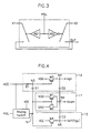
- Fig. 3 shows a detailed circuit diagram of a prior art analog switch for a TFT-LCD.
- a common electrode voltage generating wave Vcom for generating a constant voltage (VgL1 - VgL2) periodically, a gate-on voltage generating wave Vgh for generating an absolute constant voltage of VgL1 - VgL2 which causes the TFT-LCD to be turned on, and a gate-off voltage generating wave Vgl for generating an absolute constant voltage of VgL1 - VgL2 which causes the TFT-LCD to be turned off.
- Fig. 2 is comprised of analog switches 1, 3 and 5 for generating a rectangular waveform in response to an analog switching signal POL; and buffers 2, 4 and 6 for amplifying power in response to the input rectangular waveform, so that the TFT-LCD starts to be operated.
- the operation of the TFT-LCD is begun with the application of power by a user.
- the switching signal POL is then applied to the analog switches 1, 3 and 5, and the input analog swiching signal POL is converted to a rectangular wave.
- the rectangular waveform is outputted to the buffers 2. 4 and 6 and then amplified.
- the amplified waveform is outputted as each waveforms as a common electrode voltage generating waveform Vcom, a gate-on voltage generating waveform Vgh and a gate-off voltage generating waveform Vgl, each serving as the driving signal of the TFT-LCD.
- the switching signal POL is an inverse signal which causes the analog switches l, 3 and 5 to be turned on or off, and voltages V1 and V2 are potentials inputted from the analog switches, each having a different level.
- the buffer AS1 is turned on and the inverter AS2 is turned off, thereby outputting the voltage V1
- the switching signal POL is at a low state
- the buffer AS1 is turned off and the inverter AS2 is turned on, thereby outputting the voltage V2.
- the analog switch generates a rectangular waveform having the voltages V1 and V2 in response to the analog switching signal POL.
- the buffers 2, 4 and 6 each composed of the operational amplifier and the push-pull amplifier enable the power to be compensated, thereby generating the common electrode voltage generating waveform Vcom, the gate-on voltage generating waveform Vgh and the gate-off voltage generating waveform Vgl.
- TFT-LCD thin film transistor liquid crystal display
- a circuit which comprises: an analog switch for carrying out the switching operation in responce to a switching signal; a circuit connected to the analog switch for generating a common electrode voltage in response to the analog switching signal; a circuit connected to the analog switch for generating a gate-on voltage to turn on the thin film transistor by shifting the analog switching signal to a predeteminded potential and converting the shifted signal; and a circuit connected to the analog switch for generating a gate-off voltage to turn on the thin film transistor in response to the analog switching signal.
- a circuit for driving a TFT-LCD which is comprised of an analog switch 10 for carrying out the switching operation in response to a switching signal POL; a common electrode voltage generating cicuit 11 connected to the analog switch 10 for generating a common electrode voltage in response to the analog switching signal POL; a gate-on voltage generating circuit 12 connected to the analog switch 10 for generating a gate-on voltage which causes a TFT to be turned on by shifting the analog switching signal to a constant potential and converting the shifted signal; and a gate-off voltage generating circuit 13 connected to the analog switch 10 for generating a gate-off voltage which causes the TFT to be turned off in response to the analog switching signal.
- the switching signal POL as the inverse signal is inputted to the analog switch 10.
- the analog switch 10 is connected to gate terminals of a first MOS transistor M1 and a second MOS transistor M2 of the common electrode generating circuit 11, a first capacitor C1 of the gate-on voltage generating circuit 12, and a gate terminal of a fourth MOS transistor M4 of the gate-off voltage generating circuit 13.
- the common electrode voltage generating circuit 11 is connected to a second capacitor C2 of the gate-on voltage generating circuit 12 and a third capacitor C3 of the gate-off voltage generating circuit 12.
- the gate-on voltage generating circuit 12 is constructed in such a manner that anode of a first diode D1 is connected to a power source VCC and cathod is connected to the first capacitor C1 and a gate terminal of a third MOS transistor M3.
- a source terminal of the third MOS transistor M3 is connected to a power source VGG and a drain terminal of the third MOS transistor M3 is connected to the second capacitor C2.
- the gate-off voltage generating circuit 13 is constructed in such a manner that a source terminal of the fourth MOS transistor M4 is connected to a power source VEE and a drain terminal of the fourth MOS transistor M4 is connected to the third capacitor C3.
- the analog switch 10 receives the switching signal POL and creates a rectangular waveform which causes the first, second and fourth MOS transistors M1, M2 and M4 to be turned on.
- the buffer AS1 shown in Fig. 3 is turned off and the inverter AS2 is turned on, whereby the reference voltage VEE is outputted. whereas provided that the switching signal POL is high, the buffer AS1 is turned on and the inverter AS2 is turned off, whereby the voltage VCC is outputted.
- the first MOS transistor M1 of P-type of the common electrode generating circuit 11 When the analog switch 10 outputs the voltage VEE, the first MOS transistor M1 of P-type of the common electrode generating circuit 11 is turned on and the voltage VDD is outputted from the drain of the first MOS transistor M1.
- the second MOS transistor M2 of N-type of the common electrode generating circuit 11 is turned on and the ground voltage GND which is connected to the source of the second MOS transistor M2 is outputted to the drain, thereby creating the common electrode voltage generating waveform Vcom as shown in Fig. 5.
- the waveform at the first node Nl is level-shifted as much as the voltage VCC - VEE as shown in Fig. 6.
- the first diode Dl when the first node Nl outputs the voltage VEE, the first diode Dl is turned on and the third node N3 outputs the voltage VCC-V BE , whereby the first capacitor C1 charges (VCC-VBE-VEE)*Cl.
- the third MOS transistr M3 is turned on when the third node N3 has the voltage VC, and thus the voltage VGG of the source is outputted to the drain.
- the second capacitor C2 which is connected to the waveform Vcom charges C2*(VGG-VDD). This electric charge is maintained even though the third MOS transistor M3 is turned off, i.e., the third node N3 is at 2*VCC-VEE, so that the fourth nodd N4 is at VGG-VDD-GND and generates the voltage VGG-VDD.
- the gate-on voltage generating waveform Vgh is created when the above-mentioned operation is repeated as shown in Fig. 5.
- the fourth MOS transistor M4 of the gate-on voltage generating circuit 13 is turned on and the fifth node N5 shows the level VEE.
- the third capacitor C3 charges C3*(VEE-GND) and the first node N1 shows the level VEE. Accordingly, the common electrode voltage generating waveform Vcom is at the lebel VDD when the fourth MOS transistor M4 is turned off, so that the fifth node N5 shows the level VEE+VDD.
- the gate-off voltage generating waveform Vgl is created when the above-mentioned operation is repeated as shown in Fig. 5.
- the resultant circuit has some advantages which are summarized below.
- the best charateristics of the display can be realized by obtaining a maximun possible driving ability of the TFT-LCD.
Abstract
Description
- The present invention relates to a circuit for driving a thin film transistor liquid crystal display (TFT-LCD), which more specifically generates a signal capable of driving a thin film transistor liquid crystal display with low-power consumption.
- In these days, the technology of screen informations has been concentrated on the production of display devices. In particular, flat panel display devices have grown increasingly popular as substitutes for a cathod ray tubes and are now being produced on a commercial scale.
- Liquid crystal displays, among the various types of the flat panel display devices, are particularly well matched to integrated circuits because of their thinness, low-weight, low-cost, and low-power consumption. Accordingly, liquid crystal displays have been widely applied to laptopcomputors, pocket computors, automobiles, and color televisions.
- There have been generally known two methods of driving a liquid crystal display: one is an AC common driving method; another is a DC common driving method.
- The typical AC common driving method is described below with reference to the appending drawings.
- Fig. 1 is a waveform for driving a prior art TFT-LCD, Fig. 2 is a circuit block diagram for driving a prior art TFT-LCD and Fig. 3 shows a detailed circuit diagram of a prior art analog switch for a TFT-LCD.
- As shown in Fig. 1, to drive the TFT-LCD, there are basically provided a common electrode voltage generating wave Vcom for generating a constant voltage (VgL1 - VgL2) periodically, a gate-on voltage generating wave Vgh for generating an absolute constant voltage of VgL1 - VgL2 which causes the TFT-LCD to be turned on, and a gate-off voltage generating wave Vgl for generating an absolute constant voltage of VgL1 - VgL2 which causes the TFT-LCD to be turned off.
- To create such waveforms, it has been used a construction shown in Fig. 2, which is comprised of
analog switches buffers - The operation of such a constructed TFT-LCD is described below.
- The operation of the TFT-LCD is begun with the application of power by a user.
- The switching signal POL is then applied to the
analog switches - The rectangular waveform is outputted to the
buffers 2. 4 and 6 and then amplified. Next, the amplified waveform is outputted as each waveforms as a common electrode voltage generating waveform Vcom, a gate-on voltage generating waveform Vgh and a gate-off voltage generating waveform Vgl, each serving as the driving signal of the TFT-LCD. - The above-mentioned operation is described below in more detail with reference to Fig. 3.
- In this figure, the switching signal POL is an inverse signal which causes the analog switches l, 3 and 5 to be turned on or off, and voltages V1 and V2 are potentials inputted from the analog switches, each having a different level.
- As shown in this figure, provided that the switching signal POL is at a high state, the buffer AS1 is turned on and the inverter AS2 is turned off, thereby outputting the voltage V1, whereas provided that the switching signal POL is at a low state, the buffer AS1 is turned off and the inverter AS2 is turned on, thereby outputting the voltage V2.
- As a result, the analog switch generates a rectangular waveform having the voltages V1 and V2 in response to the analog switching signal POL.
- In such an operation, the
buffers - However, many disadvantages can be generated from the prior art construction. Included among these are that power consumption of the entire circuits is large because the buffer and the switch are composed of large power consumption elements such as the operational amplifier and the push-pull amplifier, and that there generates a constant offset voltage of the operational amplifier to the power source and a lowered voltage between the base and the emitter of the push-pull circuit, giving a difficulty to the generation of the rectangular wave of the power source voltage. Another disadvantge is that power consumption drastically increases because a higher voltage than a desired rectangular waveform is required.
- In view of the above, it is an object of the present invention to provide a circuit for driving a thin film transistor liquid crystal display (TFT-LCD) capable of reducing power consumption and outputting power source voltage.
- To achieve this object, according to a preferred embodiment of the present invention, a circuit is provided which comprises: an analog switch for carrying out the switching operation in responce to a switching signal; a circuit connected to the analog switch for generating a common electrode voltage in response to the analog switching signal; a circuit connected to the analog switch for generating a gate-on voltage to turn on the thin film transistor by shifting the analog switching signal to a predeteminded potential and converting the shifted signal; and a circuit connected to the analog switch for generating a gate-off voltage to turn on the thin film transistor in response to the analog switching signal.
- Fig. 1 is a waveform for driving a prior art TFT-LCD;
- Fig. 2 is a circuit block diagram for driving a prior art TFT-LCD;
- Fig. 3 is a detailed circuit diagram of a prior art analog switches;
- Fig. 4 is a circuit diagram for driving a TFT-LCD of a preferred embodiment of the present invention;
- Fig. 5 shows each waveform for driving a TFT-LCD of a preferred embodiment of the present invention; and
- Fig. 6 shows waveforms from each circuit for driving a TFT-LCD of a preferred embodiment of the present invention.
- A preferred embodiment of the present invention is described with reference to the accompanying drawings.
- As shown in Fig. 4, a circuit for driving a TFT-LCD, which is comprised of an analog switch 10 for carrying out the switching operation in response to a switching signal POL; a common electrode
voltage generating cicuit 11 connected to the analog switch 10 for generating a common electrode voltage in response to the analog switching signal POL; a gate-on voltage generatingcircuit 12 connected to the analog switch 10 for generating a gate-on voltage which causes a TFT to be turned on by shifting the analog switching signal to a constant potential and converting the shifted signal; and a gate-offvoltage generating circuit 13 connected to the analog switch 10 for generating a gate-off voltage which causes the TFT to be turned off in response to the analog switching signal. - More detailed construction is described below with the same figure.
- The switching signal POL as the inverse signal is inputted to the analog switch 10.
- The analog switch 10 is connected to gate terminals of a first MOS transistor M1 and a second MOS transistor M2 of the common
electrode generating circuit 11, a first capacitor C1 of the gate-onvoltage generating circuit 12, and a gate terminal of a fourth MOS transistor M4 of the gate-offvoltage generating circuit 13. - The common electrode
voltage generating circuit 11 is connected to a second capacitor C2 of the gate-onvoltage generating circuit 12 and a third capacitor C3 of the gate-offvoltage generating circuit 12. - Further, the gate-on voltage generating
circuit 12 is constructed in such a manner that anode of a first diode D1 is connected to a power source VCC and cathod is connected to the first capacitor C1 and a gate terminal of a third MOS transistor M3. A source terminal of the third MOS transistor M3 is connected to a power source VGG and a drain terminal of the third MOS transistor M3 is connected to the second capacitor C2. - The gate-off
voltage generating circuit 13 is constructed in such a manner that a source terminal of the fourth MOS transistor M4 is connected to a power source VEE and a drain terminal of the fourth MOS transistor M4 is connected to the third capacitor C3. - The operation of the driving circuit of this invention is described below.
- The analog switch 10 receives the switching signal POL and creates a rectangular waveform which causes the first, second and fourth MOS transistors M1, M2 and M4 to be turned on.
- In such a operation, the voltages are given by


- In the output waveform of the analog switch 10, provided that the switching signal POL is low, the buffer AS1 shown in Fig. 3 is turned off and the inverter AS2 is turned on, whereby the reference voltage VEE is outputted. whereas provided that the switching signal POL is high, the buffer AS1 is turned on and the inverter AS2 is turned off, whereby the voltage VCC is outputted.
- When the analog switch 10 outputs the voltage VEE, the first MOS transistor M1 of P-type of the common
electrode generating circuit 11 is turned on and the voltage VDD is outputted from the drain of the first MOS transistor M1. Whereas, when the analog switch 10 outputs the voltage VCC, the second MOS transistor M2 of N-type of the commonelectrode generating circuit 11 is turned on and the ground voltage GND which is connected to the source of the second MOS transistor M2 is outputted to the drain, thereby creating the common electrode voltage generating waveform Vcom as shown in Fig. 5. - Differently from the above, the waveform at the first node Nl is level-shifted as much as the voltage VCC - VEE as shown in Fig. 6.
- In detail, when the first node Nl outputs the voltage VEE, the first diode Dl is turned on and the third node N3 outputs the voltage VCC-VBE, whereby the first capacitor C1 charges (VCC-VBE-VEE)*Cl.
- Next, when the first node N1 outouts the voltage VCC, the first diode D1 is turned off, the first capacitor C1 charges (VCC-VBE-VEE)*C1 and the third node N3 outputs VCC+VCC-VBE-VEE, thereby creating the common electrode voltage generating waveform Vcom as shown in Fig. 5.
- Thus a formed waveform of the third node N3 is turned on or off the third MOS transistor M3.
- The third MOS transistr M3 is turned on when the third node N3 has the voltage VC, and thus the voltage VGG of the source is outputted to the drain.
- As a result, the second capacitor C2 which is connected to the waveform Vcom charges C2*(VGG-VDD). This electric charge is maintained even though the third MOS transistor M3 is turned off, i.e., the third node N3 is at 2*VCC-VEE, so that the fourth nodd N4 is at VGG-VDD-GND and generates the voltage VGG-VDD.
- The gate-on voltage generating waveform Vgh is created when the above-mentioned operation is repeated as shown in Fig. 5.
- Whereas, when the first node Nl is at the lebel VCC, the fourth MOS transistor M4 of the gate-on
voltage generating circuit 13 is turned on and the fifth node N5 shows the level VEE. - At this time, the third capacitor C3 charges C3*(VEE-GND) and the first node N1 shows the level VEE. Accordingly, the common electrode voltage generating waveform Vcom is at the lebel VDD when the fourth MOS transistor M4 is turned off, so that the fifth node N5 shows the level VEE+VDD.
- The gate-off voltage generating waveform Vgl is created when the above-mentioned operation is repeated as shown in Fig. 5.
- As mentioned above, it is possible to obtain the improved driving circuit of the TFT-LCD which reduces power consumption by reducing the number of the analog switch and omitting the operational amplifier and the push-pull amplifier.
- The resultant circuit has some advantages which are summarized below.
- Firstly, power consumption is reduced drastically.
- Secondly, good quality image can be obtained since the common elctrode voltage generating waveform and the gate-on voltage generating waveform are the same.
- Thirdly, the best charateristics of the display can be realized by obtaining a maximun possible driving ability of the TFT-LCD.
- Fourthly, large productivity of this circuit is permitted because there is no additional external variable resistor for controlling lebel. In other words, the number of the elements is reduced, without the requirement of the control time.
Claims (4)
- A circuit for driving a thin film transistor liquid crystal display (TFT-LCD), which comprises:an analog switch for carrying out the switching operation in responce to a switching signal;a circuit connected to the analog switch for generating a common electrode voltage in response to the analog switching signal;a circuit connected to the analog switch for generating a gate-on voltage to turn on the thin film transistor by shifting the analog switching signal to a predeteminded potential and converting the shifted signal; anda circuit connected to the analog switch for generating a gate-off voltage to turn on the thin film transistor in response to the analog switching signal.
- A circuit for driving a thin film transistor liquid crystal display of claim 1, in which the gate-on voltage generating circuit comprises:a diode;a first capacitor, connected to said diode, for receiving the signal from said diode;a MOS transistor, connected to said diode, for receiving the signal from the said diode; anda second capacitor for receiving the signal from said MOS transistor, connected to said MOS transistor and the common electrode voltage generating circuit.
- A circuit for driving a thin film transistor liquid crystal display of claim 1, in which a common electrode voltage generating circuit comprises:a P-MOS transistor; andan N-MOS transitor juxtaposed with the P-MOS transistor.
- A circuit for driving a thin film transistor liquid crystal display of claim 1, in which the gate-off voltage generating circuit comprises:a MOS transitor;a capacitor, for receiving the signal from said MOS transistor, connected to said MOS transistor and the common electrode voltage generating circuit.
Applications Claiming Priority (2)
| Application Number | Priority Date | Filing Date | Title |
|---|---|---|---|
| KR9502511 | 1995-02-11 | ||
| KR1019950002511A KR0134919B1 (en) | 1995-02-11 | 1995-02-11 | Tft driving circuit of liquid crystal display system |
Publications (2)
| Publication Number | Publication Date |
|---|---|
| EP0726558A1 true EP0726558A1 (en) | 1996-08-14 |
| EP0726558B1 EP0726558B1 (en) | 2003-05-02 |
Family
ID=19407986
Family Applications (1)
| Application Number | Title | Priority Date | Filing Date |
|---|---|---|---|
| EP96300955A Expired - Lifetime EP0726558B1 (en) | 1995-02-11 | 1996-02-12 | A circuit for driving a thin film transistor liquid crystal display |
Country Status (6)
| Country | Link |
|---|---|
| US (1) | US5754151A (en) |
| EP (1) | EP0726558B1 (en) |
| JP (1) | JP3534519B2 (en) |
| KR (1) | KR0134919B1 (en) |
| DE (1) | DE69627735D1 (en) |
| TW (1) | TW568317U (en) |
Cited By (1)
| Publication number | Priority date | Publication date | Assignee | Title |
|---|---|---|---|---|
| CN100399409C (en) * | 2002-09-25 | 2008-07-02 | 日本电气株式会社 | Driving circuit |
Families Citing this family (9)
| Publication number | Priority date | Publication date | Assignee | Title |
|---|---|---|---|---|
| KR100237887B1 (en) * | 1997-07-28 | 2000-01-15 | 구본준 | Voltage generating circuit for liquid crystal panel |
| KR100448936B1 (en) * | 1997-09-25 | 2004-11-16 | 삼성전자주식회사 | Circuit for driving liquid crystal display device to compensate gate off voltage and method for driving the same, especially supplying common voltage from a common electrode to a gate line |
| US6456281B1 (en) * | 1999-04-02 | 2002-09-24 | Sun Microsystems, Inc. | Method and apparatus for selective enabling of Addressable display elements |
| JP4200759B2 (en) * | 2002-12-27 | 2008-12-24 | セイコーエプソン株式会社 | Active matrix liquid crystal display device |
| KR100531786B1 (en) * | 2003-02-12 | 2005-11-29 | 엘지전자 주식회사 | Apparatus for driving scan driver of flat display panel |
| US7385581B2 (en) * | 2004-03-11 | 2008-06-10 | Matsushita Electric Industrial Co., Ltd. | Driving voltage control device, display device and driving voltage control method |
| KR101137844B1 (en) * | 2005-06-30 | 2012-04-23 | 엘지디스플레이 주식회사 | A liquid crystal display device |
| US7528826B2 (en) * | 2005-08-15 | 2009-05-05 | Solomon Systech Limited | Driving circuit for driving liquid crystal display panel |
| KR101330216B1 (en) * | 2006-11-02 | 2013-11-18 | 삼성디스플레이 주식회사 | Liquid crystal display |
Citations (4)
| Publication number | Priority date | Publication date | Assignee | Title |
|---|---|---|---|---|
| GB2188471A (en) * | 1986-03-19 | 1987-09-30 | Sharp Kk | L C D devices |
| EP0242468A1 (en) * | 1986-04-22 | 1987-10-28 | Seiko Instruments Inc. | Liquid crystal display device and method of driving same |
| EP0447919A2 (en) * | 1990-03-13 | 1991-09-25 | Stanley Electric Co., Ltd. | Drive circuit for dot matrix display |
| DE4306988A1 (en) * | 1992-03-05 | 1993-09-23 | Toshiba Kawasaki Kk | LCD display with active matrix - has signal line control circuits and power supply control circuits to provide signals for high quality display |
Family Cites Families (3)
| Publication number | Priority date | Publication date | Assignee | Title |
|---|---|---|---|---|
| JPH03244285A (en) * | 1990-02-22 | 1991-10-31 | Asahi Optical Co Ltd | Display element driving device |
| JPH063647A (en) * | 1992-06-18 | 1994-01-14 | Sony Corp | Drive method for active matrix type liquid crystal display device |
| JP3290772B2 (en) * | 1993-08-18 | 2002-06-10 | 株式会社東芝 | Display device |
-
1995
- 1995-02-11 KR KR1019950002511A patent/KR0134919B1/en not_active IP Right Cessation
-
1996
- 1996-02-09 JP JP02450896A patent/JP3534519B2/en not_active Expired - Lifetime
- 1996-02-12 EP EP96300955A patent/EP0726558B1/en not_active Expired - Lifetime
- 1996-02-12 DE DE69627735T patent/DE69627735D1/en not_active Expired - Lifetime
- 1996-02-12 US US08/600,110 patent/US5754151A/en not_active Expired - Lifetime
- 1996-04-09 TW TW088217027U patent/TW568317U/en not_active IP Right Cessation
Patent Citations (4)
| Publication number | Priority date | Publication date | Assignee | Title |
|---|---|---|---|---|
| GB2188471A (en) * | 1986-03-19 | 1987-09-30 | Sharp Kk | L C D devices |
| EP0242468A1 (en) * | 1986-04-22 | 1987-10-28 | Seiko Instruments Inc. | Liquid crystal display device and method of driving same |
| EP0447919A2 (en) * | 1990-03-13 | 1991-09-25 | Stanley Electric Co., Ltd. | Drive circuit for dot matrix display |
| DE4306988A1 (en) * | 1992-03-05 | 1993-09-23 | Toshiba Kawasaki Kk | LCD display with active matrix - has signal line control circuits and power supply control circuits to provide signals for high quality display |
Cited By (1)
| Publication number | Priority date | Publication date | Assignee | Title |
|---|---|---|---|---|
| CN100399409C (en) * | 2002-09-25 | 2008-07-02 | 日本电气株式会社 | Driving circuit |
Also Published As
| Publication number | Publication date |
|---|---|
| EP0726558B1 (en) | 2003-05-02 |
| KR0134919B1 (en) | 1998-04-25 |
| US5754151A (en) | 1998-05-19 |
| KR960032280A (en) | 1996-09-17 |
| JP3534519B2 (en) | 2004-06-07 |
| DE69627735D1 (en) | 2003-06-05 |
| TW568317U (en) | 2003-12-21 |
| JPH08248390A (en) | 1996-09-27 |
Similar Documents
| Publication | Publication Date | Title |
|---|---|---|
| US8085028B2 (en) | Method of driving a semiconductor device | |
| KR100348644B1 (en) | Voltage Multiplier Having An Intermediate Tap | |
| JP4576652B2 (en) | Liquid crystal display | |
| CN1855212B (en) | Display driver circuit and display apparatus | |
| JP2005070801A (en) | Driving device of of thin film transistor liquid crystal display device | |
| CN112687227A (en) | Display panel and display device | |
| KR20080011896A (en) | Gate on voltage generation circuit and gate off voltage generation circuit and liquid crystal display having the same | |
| US6392627B1 (en) | Liquid crystal display device and driver circuit thereof | |
| EP0726558B1 (en) | A circuit for driving a thin film transistor liquid crystal display | |
| KR20050070195A (en) | Shift register | |
| TWI415083B (en) | A semiconductor integrated circuit and a semiconductor integrated circuit for driving a liquid crystal display | |
| KR101027827B1 (en) | Shift register and method for driving the same | |
| KR20070007591A (en) | Voltage generator for flat panel display apparatus | |
| KR100608743B1 (en) | Driving apparatus in a liquid crystal display | |
| CN107633804B (en) | Pixel circuit, driving method thereof and display panel | |
| JP3611518B2 (en) | LCD panel scanning line driver | |
| JPH09230829A (en) | Output circuit for source driver | |
| JP2002140041A (en) | Driving circuit for display device | |
| CN110401424B (en) | Operational amplifier | |
| US20070268282A1 (en) | System for driving columns of a liquid crystal display | |
| KR101073263B1 (en) | Shift register and method for driving the same | |
| CN214624389U (en) | Display panel and display device | |
| JPH07199156A (en) | Liquid crystal display device | |
| JP2000132147A (en) | Stabilizing circuit and power supply circuit using it | |
| JP4269457B2 (en) | Power supply device, display device, and driving method of display device |
Legal Events
| Date | Code | Title | Description |
|---|---|---|---|
| PUAI | Public reference made under article 153(3) epc to a published international application that has entered the european phase |
Free format text: ORIGINAL CODE: 0009012 |
|
| AK | Designated contracting states |
Kind code of ref document: A1 Designated state(s): DE FR GB |
|
| 17P | Request for examination filed |
Effective date: 19970122 |
|
| 17Q | First examination report despatched |
Effective date: 20000425 |
|
| GRAG | Despatch of communication of intention to grant |
Free format text: ORIGINAL CODE: EPIDOS AGRA |
|
| GRAG | Despatch of communication of intention to grant |
Free format text: ORIGINAL CODE: EPIDOS AGRA |
|
| GRAH | Despatch of communication of intention to grant a patent |
Free format text: ORIGINAL CODE: EPIDOS IGRA |
|
| GRAH | Despatch of communication of intention to grant a patent |
Free format text: ORIGINAL CODE: EPIDOS IGRA |
|
| GRAA | (expected) grant |
Free format text: ORIGINAL CODE: 0009210 |
|
| AK | Designated contracting states |
Designated state(s): DE FR GB |
|
| PG25 | Lapsed in a contracting state [announced via postgrant information from national office to epo] |
Ref country code: FR Free format text: LAPSE BECAUSE OF FAILURE TO SUBMIT A TRANSLATION OF THE DESCRIPTION OR TO PAY THE FEE WITHIN THE PRESCRIBED TIME-LIMIT Effective date: 20030502 |
|
| REG | Reference to a national code |
Ref country code: GB Ref legal event code: FG4D |
|
| REF | Corresponds to: |
Ref document number: 69627735 Country of ref document: DE Date of ref document: 20030605 Kind code of ref document: P |
|
| PG25 | Lapsed in a contracting state [announced via postgrant information from national office to epo] |
Ref country code: DE Free format text: LAPSE BECAUSE OF FAILURE TO SUBMIT A TRANSLATION OF THE DESCRIPTION OR TO PAY THE FEE WITHIN THE PRESCRIBED TIME-LIMIT Effective date: 20030805 |
|
| PLBE | No opposition filed within time limit |
Free format text: ORIGINAL CODE: 0009261 |
|
| STAA | Information on the status of an ep patent application or granted ep patent |
Free format text: STATUS: NO OPPOSITION FILED WITHIN TIME LIMIT |
|
| 26N | No opposition filed |
Effective date: 20040203 |
|
| EN | Fr: translation not filed | ||
| REG | Reference to a national code |
Ref country code: GB Ref legal event code: 732E Free format text: REGISTERED BETWEEN 20130307 AND 20130313 |
|
| PGFP | Annual fee paid to national office [announced via postgrant information from national office to epo] |
Ref country code: GB Payment date: 20150122 Year of fee payment: 20 |
|
| REG | Reference to a national code |
Ref country code: GB Ref legal event code: PE20 Expiry date: 20160211 |
|
| PG25 | Lapsed in a contracting state [announced via postgrant information from national office to epo] |
Ref country code: GB Free format text: LAPSE BECAUSE OF EXPIRATION OF PROTECTION Effective date: 20160211 |