EP0725496B1 - Frequency offset cancellation apparatus - Google Patents
Frequency offset cancellation apparatus Download PDFInfo
- Publication number
- EP0725496B1 EP0725496B1 EP19960101276 EP96101276A EP0725496B1 EP 0725496 B1 EP0725496 B1 EP 0725496B1 EP 19960101276 EP19960101276 EP 19960101276 EP 96101276 A EP96101276 A EP 96101276A EP 0725496 B1 EP0725496 B1 EP 0725496B1
- Authority
- EP
- European Patent Office
- Prior art keywords
- signal
- frequency offset
- vector
- detection
- multiplication
- Prior art date
- Legal status (The legal status is an assumption and is not a legal conclusion. Google has not performed a legal analysis and makes no representation as to the accuracy of the status listed.)
- Expired - Lifetime
Links
Images


Classifications
-
- H—ELECTRICITY
- H04—ELECTRIC COMMUNICATION TECHNIQUE
- H04B—TRANSMISSION
- H04B1/00—Details of transmission systems, not covered by a single one of groups H04B3/00 - H04B13/00; Details of transmission systems not characterised by the medium used for transmission
- H04B1/69—Spread spectrum techniques
- H04B1/707—Spread spectrum techniques using direct sequence modulation
Definitions
- the present invention relates to a frequency offset cancellation apparatus which is utilized for a receiver and the like used in a base station of a mobile communication system using a Code-Division Multiple Access (CDMA), and which serves to cancel a frequency offset produced in transmission paths lines.
- CDMA Code-Division Multiple Access
- frequency offsets occur from Doppler Effect due to multiple transmitting paths and from the residual frequency errors of oscillators in receivers and transmitters in spite of their cancellation by demodulators, and therefore removal of frequency offsets has been heretofore performed.
- correction of the frequency offsets must be performed.
- US-A-5,361,276 discloses an all digital maximum likelihood based spread spectrum receiver which applies a presuming maximum likelihood technique of received signals for the estimation of the frequency offset.
- Fig. 1 is a block diagram showing a constitution of another conventional frequency offset cancellation apparatus.
- the receiver shown in Fig. 1 is installed in a CDMA base station that comprises a plurality of correlators to cope with multi-paths. This receiver receives signals provided from the same transmitter with a plurality of antennas (not shown).
- a frequency conversion circuit 90 is provided with a received radio-frequency (RF) signal obtained by synthesizing the signals from the same transmitter.
- the RF signal is converted down with a local oscillating signal from a local oscillator 91.
- a base band (BB) signal obtained after mixing is provided to correlation circuits 93a, 93b,...,93n.
- BB base band
- the correlation circuits 93a, 93b,..., and 93n despread with spread codes shifted from each other with respect to time.
- the obtained correlation signals from the correlation circuits 93a, 93b,...., and 93n are provided to detection circuits 94a, 94b,...., and 94n.
- the detection signals from the detection circuits 94a, 94b,...., and 94n are combined by a combining circuit 95.
- the output signal (combined signal) is provided to a frequency offset detecting circuit 92.
- the known portion of the pilot signal which is the known portion in the output signal is compared with the theoretical value whereby the frequency offset is detected.
- the voltage of the frequency offset value is provided to a local oscillator 91 such as a voltage controled oscillator (VCO) and the like. The oscillating frequency thereof is adjusted and the frequency offset is corrected (canceled).
- VCO voltage controled oscillator
- Fig. 2 is a block diagram showing another constitution of the conventional offset correction apparatus.
- the constitution shown in Fig. 2 shows a receiver of a CDMA base station apparatus which utilizes a received high frequency signal by dividing it into a plurality of channels.
- a plurality of antennas receive a signal from the same transmitter.
- a received radio frequency (RF) signal such as a synthesized received signal and the like is provided to a frequency converting circuit 100.
- a base band (BS) signal obtained by converting down with a local oscillating signal from a local oscillator 101 is divided into a plularity of channels.
- the divided signals are provided to receiving demodulation sections of channels A to N, each of which transmits the output signal respectively.
- Each of the receiving demodulation sections A to N of the channels has the same constitution and performs the same operation.
- a base band signal is provided to correlation circuits 104a, 104b,...., and 104n through a frequency offset correction circuit 103.
- the correlation circuits 104a, 104b,..., and 104n perform despreading with the diffusion symbols which are shifted from each other with respect to time.
- the obtained correlation signals from the correlation circuits 104a, 104b,...., and 104n are provided to corresponding detection circuits 105a, 105b,...., and 105n, respectively.
- the respective detection signals from the detection circuits 105a, 105b,...., and 105n are combined by a combining circuit 106.
- the obtained output signal (combined signal) is provided to a frequency offset detection circuit 102.
- the frequency offset detection circuit 102 compares the known pilot signal portion of the output signal with the theoretical value to detect the frequency offset.
- the value of the frequency offset is provided to the frequency offset cancellation circuit 103.
- the frequency offset of the base band signal is canceled.
- a communication path frequency offset correction apparatus As a proposal to cancel such a frequency offset, a communication path frequency offset correction apparatus is known, which is disclosed in JP-A-62-219832.
- this apparatus when noise in the modulation signal during a secret communication, i.e. the frequency offset, becomes larger, the level of the noise is detected, and controlled so as to be lowered.
- the conventional frequency offset correction apparatus is not able to use the received high frequency signal of the receiver shown in Fig. 1 in such a manner that it is divided for each of the channels.
- the communication path frequency offset correction apparatus disclosed in JP-A-62-219832 is also not able to use the received high frequency offset cancellation signal by dividing it for each of the channels.
- the receiver of the code division multi-access (CDMA) base station apparatus shown in Fig. 2 is able to use the received high frequency signal by dividing it into a plurality of channels, the base band signal obtained by the frequency offset cancellation circuit 103 is at a high speed. Therefore, it needs very many computations which take a long time, when the frequency offset is canceled by sampling. For example, in case of a chip rats of 128 chips/symbol, a computation rate of 7.68 M chips/sec is needed even when the symbol rate is 60K/sec. Accordingly, there is a drawback in that data transmission at a higher speed is impossible.
- CDMA code division multi-access
- the object of the present invention is to provide a frequency offset cancellation apparatus which eliminates the drawbacks of the prior art, shortens the processing time by reducing the quantity of the computations for the frequency offset cancellation thereby achieving high speed data transmission. This object is achieved with the features of the claims.
- a frequency offset correction apparatus of a first aspect of the present invention comprises a receiving means for outputting a base band signal obtained by demodulating a received high frequency signal; an A/D converting means for converting the base band signal inputted from the receiving means to a digital signal; a plurality of correlation processing means for producing correlation signals obtained by despreading the digital base band signal received from the A/D converting means with spread codes which are shifted from the inputted base band signal with respect to time; a plurality of detecting means for detecting the correlation signals inputted from corresponding correlation processing means; a combining means for synthesizing detection signals inputted from detection means by adding them; a frequency offset detection means for detecting the value of a frequency offset of a signal from the combining means, using a known portion of the signal; and a frequency offset cancellation means for canceling the frequency offset from the output of said combining means, based on the value of the frequency offset which is detected by the frequency offset detection means.
- a frequency offset cancellation apparatus of a second aspect of the present invention has a feature that each of the aforementioned detection means comprises a delay circuit which delays the correlation signal from the corresponding correlation processing means for an equivalent amount of one symbol length; and a multiplication section which multiplies the correlation signal inputted from the corresponding correlation processing means by the correlation signal delayed for the equivalent amount of one symbol length inputted from the delay circuit, to produce a detection signal, and performs a delay detection.
- a frequency offset cancellation apparatus of a third aspect of the present invention has a feature that each of the aforementioned detection means comprises a detection circuit; and a multiplication section which delays an estimated fading vector for the equivalent amount of one symbol length, converts the fading vector into a conjugate complex form, and produces a detection signal obtained by multiplying the fading vector converted into the conjugate complex form by a correlation signal inputted from a correlation circuit, and performs a coherent detection.
- a frequency offset cancellation apparatus of a fourth aspect of the present invention has a feature that the aforementioned frequency offset detection means comprises a known signal theoretical value generating section which generates the theoretical value of the known signal; a first conjugation section which produces a signal obtained by converting the theoretical value of the known signal from the known signal theoretical value generating section into a conjugate complex form; a third multiplication section which detects the phase shift of the known portion of the signal combined by the combining means, inputted from the signal converted into the conjugate complex form by the first conjugation section; an n symbol delay section which delays a phase shifted signal from the third multiplication section for the equivalent amount of n symbols; a second conjugation section which converts the phase shifted signal, delayed for the equivalent amount of n symbols by the n symbol delay section, into the conjugate complex form; a fourth multiplication section which multiplies the phase shifted signal from the multiplication section by the signal converted into the conjugate complex form from the second conjugation section; an integration section which integrates rotation vectors equivalent to the number of symbols obtained by
- a frequency offset cancellation apparatus of a fifth aspect of the present invention has a feature that the aforementioned frequency offset detection means comprises a fifth multiplication section which multiplies a frequency offset cancellation vector by a frequency offset vector; a holding section which holds the frequency offset cancellation vector; a conjugation section which converts the vector, obtained by the fifth multiplying section, into a conjugate complex form; and a sixth multiplication section which produces an output signal obtained by multiplying the vector, converted into the conjugate complex form by the conjugation section, by the combined signal from the combining means.
- a frequency offset cancellation apparatus of a sixth aspect of the present invention has a feature that the aforementioned frequency offset cancellation means comprises a conjugation section which converts a frequency offset vector from a frequency offset detection means into a conjugate complex form; and a seventh multiplication section which produces an output signal obtained by canceling a frequency offset, the frequency offset being obtained by multiplying a signal synthesized by a combining means by a frequency offset vector converted into a conjugate complex form by the conjugation section.
- frequency offset correction apparatuses of the present invention can be used preferably for a symbol dividing multiple transmitting demodulator.
- the frequency offset correction apparatuses of the first to sixth aspects of the present invention are applied to the symbol dividing multiple transmitting demodulator.
- the frequency offset correction apparatuses of the first to sixth aspects of the present invention detect the correlation signals which are obtained by despreading the sampled base band signal with spread codes shifted from each other with respect to time, and sum up the detected signals to combine them.
- the value of the frequency offset is detected using the known combined signal.
- the detected frequency offset is corrected by canceling. Specifically, the frequency offset is detected by the combined data of a low speed, and the output signal is rotated reversely so that the frequency offset is canceled.
- the frequency offset cancellation apparatus of the present invention can cope with the case where one received high frequency signal is used for a plurality of channels.
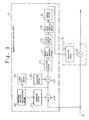
- Fig. 3 is a block diagram showing a constitution of a first embodiment of a frequency offset cancellation apparatus based on the present invention.
- the frequency offset cancellation apparatus of the first embodiment is arranged in a receiver of a CDMA base station apparatus, the receiver detects a received high frequency signal by a delay-detection and divides it into a plurality of channels.
- a frequency converting circuit 1 and a local oscillator 2 are arranged.
- the frequency converting circuit 1 receives signals from the same transmitter through a plurality of antennas (not shown ), converting down the received radio frequency signal (RF signal ) such as the combined received signal with a local oscillating signal to provide a base band ( BB ) signal, the base band signal being subjected to frequency conversion.
- the local oscillator 2 transmits the aforementioned local oscillating signal to the frequency conversion circuit 1.
- an A/D converter 3 and receiving/demodulation sections A to N are arranged.
- the A/D converter 3 quantizes and samples, i.e. digitizes, the base band signal, and each of the receiving/demodulation sections A to N has the same constitution and performs the demodulation for each channel.
- a frequency offset detection circuit 7 and a frequency offset cancellation circuit 8 are arranged.
- the frequency offset detection circuit 7 compares the known pilot signal which is the known portion of an output signal from the receiving/demodulation section with a theoretical value, thereby detecting the frequency offset.
- the frequency offset cancellation circuit 8 reversely rotates the output signal and cancels the frequency offset based on the value of the frequency offset provided from the frequency offset detection circuit 7.
- Each of the receiving/demodulation sections A to N comprises correlation circuits 4a, 4b,...., and 4n, detection circuits 5a, 5b,...., and 5n, and a combining circuit 6.
- Each of the correlation circuits 4a, 4b,..., and 4n produces a correlation value signal obtained by despreading the digitized base band signal from the A/D converter 3 using spread codes shifted from each other with respect to time.
- Each of the detection circuits 5a, 5b,..., and 5n produces the detection signal by detecting the corresponding correlation value signal.
- the combining circuit 6 combines the detection signals from the detection circuits 5a, 5b,...., and 5n by combining them and outputs the combined signal.
- Fig. 4 shows a detailed block diagram of the detection circuits 5a, 5b,..., and 5n of Fig. 3.
- each of the detection circuits 5a, 5b,...., and 5n comprises a delay circuit 14, a conjugation section 15 and multiplication section 16.
- Delay circuit 14 delays the correlation value signal supplied from the corresponding one among the correlation circuits 4a, 4b,...., and 4n for one symbol length.
- the conjugaton section 15 complex conjugates the signal delayed by one symbol length.
- the conjugation section 15 converts the signal delayed by one symbol length into a conjugate complex form.
- Multiplication section 16 multiplies the correlation value signal from the corresponding correlation circuit by the signal complex conjugated by the conjugation section, and produces a multiplication signal (detection signal).
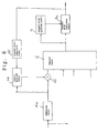
- Fig. 5 shows a detailed block diagram of frequency offset detection circuit 7 and frequency offset correction circuit 8 of Fig. 3.
- a known signal theoretical value generating section 20 and a conjugation section 21 are arranged in the frequency offset detection circuit 7.
- Known signal theoretical value generating section 20 generates a theoretical value of the known signal.
- Conjugation section 21 converts the theoretical value of the known signal from known signal theoretical value generating section 20 into the conjugate complex form and provides it to a multiplication section 22 which is described later.
- Multiplication section 22 detects the phase shifting between the known portion of the signal obtained by combining the detection signals and the signal converted into the conjugate complex form.
- N-symbol delay section 23 delays a phase shifted signal for n symbol lengths.
- Conjugate section 24 converts the phase shifted signal delayed for n symbol lengths into the conjugate complex form.
- Multiplication section 25 multiplies the phase shifted signal by the conjugate complex signal from conjugation section 24.
- Integration section 26 integrates rotation vectors equivalent to the number of the symbols that is obtained by subtracting n from the number of the symbols.
- frequency offset detection circuit 7 comprises a vector/angle converting section 27, a 1/n multiplication section 28, an angle/vector converting section 29, and a holding section 30.
- Vector/angle converting section 27 converts the integrated vectors into angles.
- 1/n multiplication section 28 divides the rotation angle among the n symbols by the number of the symbols to obtain the rotation angle per one symbol.
- Angle/vector converting section 29 converts the rotation angle per one symbol into the frequency offset vector of the norm " 1 ".
- Holding section 30 holds the frequency offset vector until the subsequent frequency offset vector is obtained.
- the frequency offset cancellation circuit 8 comprises a conjugation section 31 and a multiplication section 32.
- Conjugation section 31 converts the frequency offset vector inputted from frequency offset detection circuit 7 into the conjugate complex form.
- Multiplication section 32 multiplies the signal which is obtained by the combining circuit 6 by the frequency offset vector received from the conjugation section 31, and transmits an output signal which is the frequency for which the offset has been corrected by the multiplication.
- the received radio frequency signal (RF signal) is converted down with the local oscillation signal inputted from local oscillator 2 by the frequency converting circuit 1 to produce the base band (BB) signal.
- the base band signal is sampled by the A/D converter 3, and it is provided to each of the receiving/demodulation sections A to N.
- the sampling frequency of the A/D converter 3 is the same as that of the chip rate.
- correlation circuits 4a, 4b,...., and 4n provide the correlation value signals to the corresponding detection circuits 5a, 5b,...., and 5n, which are obtained by despreading the base band signal with the spread code shifted from each other with respect to time. It should be noted that the correlation signals are obtained by integrating the quantity equivalent to one symbol that is given by multiplying the digitized base band signal from the A/D converter 3 by the spread signal.
- detection circuits 5a, 5b,.... and and the detection is performed by multiplying the conjugate complex of the signal preceding by one symbol.
- delay circuits 14 shown in Fig. 4 the correlation value signal from each of correlation circuits 4a, 4b,...., , and 4n is delayed for one symbol length , and the delayed correlation value signal is multiplied by the correlation value signal by multiplication section 16.
- the detection signals from detection circuits 5a, 5b,...., and 5n are synthesized by the summing/synthesizing or combining circuit 6, and the combined output signal is produced therefrom.
- This output signal is provided to frequency offset detection circuit 7.
- the known pilot signal portion of the output signal is compared with the theoretical value. Hence, the frequency offset of the output signal is detected, and the frequency offset is provided to frequency offset correction circuit 8.
- frequency offset correction circuit 8 the output signal from combining circuit 6 is reversely rotated based on the value of the frequency offset from frequency offset detection circuit 7. Hence, the frequency offset of the output signal is corrected. Subsequently, the output signal is sent out from frequency offset correction circuit 8.
- the conjugation section 21 converts the theoretical value of the known signal received from known signal theoretical generating section 20 into the conjugate complex form.
- Multiplication section 22 multiplies the signal converted into the conjugate complex form by the known portion of the combined signal inputted from combining circuit 6. Hence, the phase shift is detected.
- n symbol delay circuit 23 delays the signal, representing the phase shift, for n symbols. This delayed signal is converted into the conjugate complex form by conjugation section 24.
- Multiplication section 25 multiplies the delayed signal converted into the conjugate complex form by the signal representing the phase shift inputted from multiplication section 22.
- integration section 26 integrates the rotation vector equivalent to the number of the symbols that is obtained by substracting n from the number of the symbols of the known signal.
- the vector integrated by integration section 26 is converted into an angle by vector/angle converting section 27.
- the rotation angle between the n symbols is given from this conversion. This angle is divided by the number of the symbols by 1/n multiplication section 28, thereby obtaining the rotation angle per one symbol. Further, the rotation angle per one symbol is converted into the frequency offset vector of norm " 1 " by angle/vector converting section 29.
- the obtained frequency offset vector is held by the holding section 30 until the subsequent frequency offset vector is obtained. In the manner as described above, the frequency offset is detected.
- the rotation vector between the first and third symbols of the pilot signal is obtained.
- the rotation vector between the second and fourth symbols of the pilot signal is obtained.
- the rotation vector between the third and fifth symbols of the pilot signal is obtained.
- frequency offset correction circuit 8 since the signal that is combined in the frequency offset detection circuit 7 is rotated by the quantity equivalent to the frequency offset, we make all the symbols of signals reversely rotate by the quantity equivalent to the frequency offset. Specifically, the frequency offset vector is converted into the conjugate complex form by conjugation section 31, and it is multiplied by the combined signal from combining circuit 6 by multiplication section 32. Thus, the output signal wherein the frequency offset is corrected is obtained.
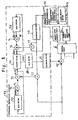
- Fig. 6 is a block diagram showing a constitution of the second embodiment of the frequency offset cancellation apparatus based on the present invention.
- the frequency offset cancellation apparatus shown in Fig. 6 being employed in the receiver of the CDMA base station apparatus, performs a sequential follow-up synchronizing detection for the received high frequency signal and divides the received high frequency signal into a plurality of channels.
- the constitution of frequency offset cancellation circuit 8a of the second embodiment shown in Fig. 7 is similar to the construction of frequency offset cancellation circuit 8 of the first embodiment shown in Fig. 5.
- the detailed constitution of a frequency offset cancellation/decision circuit 45 is shown in Fig. 8, and the frequency offset cancellation/decision circuit 45 performs the frequency offset cancellation and decision for the output signal from the frequency offset cancellation circuit 8a.
- a coherent detection circuit 44 corresponding to detection circuits 5a, 5b,...., and 5n of the first embodiment and a multiplication section 46.
- the coherent detection circuit 44 performs a coherent detection using RLS (Recursive Least Squares) estimate for phase and amplitude, and the multiplication section 46 produces a detection signal.
- the detection signal is obtained by multiplying the correlation signal by the signal received from a conjugation section 81 described later. This signal is given by delaying the estimated fading vector Z (n) for one symbol length and by converting it into the conjugate complex form. Since the function blocks other than the function blocks described above are the same as those of Fig. 3, explanations are omitted.
- Fig. 7 is a detailed block diagram of the frequency offset cancellation circuit 8a of Fig. 6.
- frequency offset cancellation circuit 8a comprises a multiplication section 61 which multiplies the frequency offset correction vector by the frequency offset vector, and a holding section 62 which holds the frequency offset cancellation vector. Furthermore, frequency offset cancellation circuit 8a comprises a conjugation section 63 which converts the vector multiplied by multiplication section 61 into the conjugate complex form, and a multiplication section 64 which multiplies the vector converted into the conjugate complex form by the signal obtained by adding and synthesizing.
- Fig. 8 is a detailed block diagram of coherent detection circuit 44 and frequency offset cancellation/decision circuit 45, shown in Fig. 6.
- coherent detection circuit 44 comprises a delay section 70 which delays a combined signal ⁇ i (n), and a multiplication section 71 which multiplies the weighting correlation ⁇ i (n - 1) by ⁇ , where ⁇ i (n-1) is the sum of the correlation value signal i and the decision signal o accumulated until the last symbol, and outputs the multiplication result.
- coherent detection circuit 44 comprises an addition section 72 which adds the correlation value signal i at the last symbol to the signal multiplied by ⁇ by the multiplication section 71, a multiplication section 73 which multiplies the correlation signal i by the decision signal o converted into the conjugate complex form, a delay section 74 which delays the signal ⁇ i (n) obtained by adding the decision signal o to the signal which is obtained by multiplying the weighting sum ⁇ i (n - 1) by ⁇ , multiplication section 75 which multiplies the weighting sum ⁇ i (n-1) of norm of decision signal o accumulated until the last symbol by ⁇ and a summing section 76 which adds the decision signal o to the weighting sum ⁇ i (n-1) by ⁇ 1.
- coherent detection circuit 44 there are provided a multiplication section 77 which multiplies the decision signal by the signal converted into the conjugate complex form, and a conjugation section 78 which performs the conjugate complex conversion to obtain a cross correlation between the decision signal o and the correlation value signal i.
- coherent detection circuit 44 comprises a division section 79 which divides the signal ⁇ i (n) by the signal ⁇ i (n) to obtain the estimated fading vector Zi (n), a delay section 80 which delays the estimated fading vector Zi (n) by the quantity equivalent to one symbol length, and a conjugation section 81 which converts the estimated fading vector Zi (n), delayed for one symbol length, into the conjugate complex form.
- the frequency offset cancellation/decision circuit 45 comprises a frequency offset correction section 82 and a signal decision section 83 which obtains the decision signal o multiplied by the frequency offset vector in the case other than the known signal.
- the frequency offset cancellation section 82 rotates the theoretical value by the quantity equivalent to the frequency offset to output it as the decision'signal o in the known pilot signal and the like, and decides whether the output signal through the frequency offset cancellation circuit 8a is positive or negative, in the case other than the known signal.
- the operations of the second embodiment performed by frequency converting circuit 1 to correlation circuit 4a in Fig. 6 are the same as those of Fig. 3.
- the received high frequency signal is subject to frequency conversion.
- the obtained base band signal is converted into the digital signal.
- the digital signal is demodulated by the receiving demodulation processing sections having the same constitution, which perform the demodulations of the signals distributed to the corresponding channels.
- the receiving demodulation processing sections are the same as those in Fig. 3.
- the frequency offset is detected by frequency offset detection circuit 7, and the output signal, in which the frequency offset is canceled based on the value of the frequency offset by frequency offset cancellation circuit 8a, is transmitted.
- the coherent detection circuit decides on a signal o estimated as being transmitted (received high frequency signal) based on a detected signal y shown in Fig. 8. Calculating correlation between this decision signal o and the correlation value signal i, the coherent detection circuit estimates a fading signal sequentially. Multiplying this estimation signal Z by the correlation signal i, the coherent detection circuit performs the coherent detection using RLS estimation for phase and amplitude.
- the correlation signal i is multiplied by the signal which is converted into the conjugate complex form by conjugation section 78 using multiplication section 73.
- the weighting correlation sum ⁇ i (n - 1) of the preceding correlation signal i and the decision-signal o accumulated until the last symbol is multiplied by ⁇ using multiplication section 71.
- the signal from the multiplication section 71 and the signal from the multiplication section 73 are added by addition section 72.
- the sum ⁇ i (n) is obtained, and it is delayed by delay section 70.
- the sum ⁇ i (n) is used as ⁇ i (n - 1) for the computation at the time of the subsequent symbol.
- multiplication section 77 multiplies the decision signal o by the signal converted into the conjugate complex form by conjugation section 78.
- the multiplication section 75 multiplies the norm weighting sum S (n - 1) of the decision signal o accumulated until the last symbol by ⁇ .
- Addition section 76 adds the signal inputted from multiplication section 77 to the signal inputted from multiplication section 75 to obtain the sum ⁇ i (n).
- the sum ⁇ i (n) is delayed by delay section 74.
- the sum ⁇ i (n) is used as ⁇ i (n - 1) for the computation at the time of the subsequent symbol.
- the estimation signals are produced according to the data of several past symbols.
- the fading vector Zi(n) is obtained.
- the value of the estimated fading vector Z (n) is delayed for one symbol length using the delay section 80, converted into the conjugate complex form using the conjugation section 81 and multiplied by the correlation value signal i using multiplication section 46 so that the detection output can be obtained.
- Decision signal o which is necessary for the operation of the coherent detection in coherent detection circuit 44 is inputted from frequency offset cancellaton/decision circuit 45.
- frequency offset correction/decision circuit 45 the signal obtained by rotating the theoritical value of the known pilot signal and the like by the angle of the frequency offset is defined as the decision signal.
- an output signal for which it is decided whether it is positive or negative and which is rotated by the amount of the frequency offset quantity is defined as a decision signal o.
- signal decision section 83 rotates the theoretical value of the known signal portion such as the pilot signal and the like by an equivalent amount of the frequency offset, and the rotated theoretical value is used as the decision signal o. In other cases than the known signal, it is decided whether the output signal passing through combining circuit 6 and frequency offset cancellation circuit 8a is positive or negative. Further, the decided output signal is multiplied by the frequency offset vector using frequency offset cancellation section 82, and it is used as the decision signal o.
- the coherent detection signal which is outputted from coherent detection circuit 44 and multiplication section 46 is added to other coherent detection signals by combining circuit 6 to be combined. Since this data rotates according to the frequency offset as in the first embodiment, it is reversely rotated by the equivalent amount of the frequency offset which is detected by frequency offset cancellation circuit 8a so that it is corrected.
- frequency offset detection circuit 7 shown in Fig. 7 is similar to that of the first embodiment shown in Fig. 5.
- frequency offset cancellation circuit 8a the frequency of the signal obtained after the signals are combined by combining circuit 6 is offset by the equivalent amount of the frequency offset.
- the frequency offset cancellation vector held by holding section 62 is multiplied by the frequency offset vector using multiplication section 61. Then, the vector converted into the conjugate complex form by conjugation section 63 is multiplied by the signal which is obtained by combining using multiplication section 64.
- the same signal is obtained as the case where the frequency offset is corrected in each of the paths (receiving high frequency signal). Specifically, since the correction of the frequency offset is performed once per one symbol, the quantity of the computations is reduced, thereby decreasing the processing time, compared with the case where the frequency offset corrections are performed for each path and the case where the frequency offset cancellation is performed as to the base band signal.
- the frequency offset is detected by low speed data obtained by combining and the frequency offset is canceled by rotating reversely the output signal.
- the frequency offset is the same in each of the paths, even when the number of the antennas is increased in order to realize a multipath, the quantity of the computations at the time of the cancellation of the frequency offset is reduced. The processing time is reduced so that for example, data transmission at a higher speed becomes possible. Furthermore when the quantity of the computations is limited, more paths can be combined so that the quality of the receiving signal is increased.
- the frequency offset cancellation apparatus of the present invention can cope with the case where one receiving high frequency signal is distributed into the plurality of the channels.
- the frequency offset cancellation apparatuses of the present invention shown in Fig. 3 to 7, there is performed a detection of the respective correlation signals which are obtained by despreading the digitized base band signal with spread codes shifted from each other with respect to time and a synthesis of the detected signals by adding.
- the value of the frequency offset is detected by utilizing the known portion of the combined signal and the detected frequency offset is canceled.
Description
- The present invention relates to a frequency offset cancellation apparatus which is utilized for a receiver and the like used in a base station of a mobile communication system using a Code-Division Multiple Access (CDMA), and which serves to cancel a frequency offset produced in transmission paths lines.
- In this kind of receiver, frequency offsets occur from Doppler Effect due to multiple transmitting paths and from the residual frequency errors of oscillators in receivers and transmitters in spite of their cancellation by demodulators, and therefore removal of frequency offsets has been heretofore performed. In this case, since a transmitting error occurs in transmitted information due to a detection error, correction of the frequency offsets must be performed.
- US-A-5,361,276 discloses an all digital maximum likelihood based spread spectrum receiver which applies a presuming maximum likelihood technique of received signals for the estimation of the frequency offset.
- Fig. 1 is a block diagram showing a constitution of another conventional frequency offset cancellation apparatus. The receiver shown in Fig. 1 is installed in a CDMA base station that comprises a plurality of correlators to cope with multi-paths. This receiver receives signals provided from the same transmitter with a plurality of antennas (not shown). A
frequency conversion circuit 90 is provided with a received radio-frequency (RF) signal obtained by synthesizing the signals from the same transmitter. The RF signal is converted down with a local oscillating signal from alocal oscillator 91. A base band (BB) signal obtained after mixing is provided tocorrelation circuits 93a, 93b,...,93n. Thecorrelation circuits 93a, 93b,..., and 93n despread with spread codes shifted from each other with respect to time. The obtained correlation signals from thecorrelation circuits 93a, 93b,...., and 93n are provided todetection circuits - The detection signals from the
detection circuits circuit 95. The output signal (combined signal) is provided to a frequencyoffset detecting circuit 92. The known portion of the pilot signal which is the known portion in the output signal is compared with the theoretical value whereby the frequency offset is detected. The voltage of the frequency offset value is provided to alocal oscillator 91 such as a voltage controled oscillator (VCO) and the like. The oscillating frequency thereof is adjusted and the frequency offset is corrected (canceled). - Fig. 2 is a block diagram showing another constitution of the conventional offset correction apparatus.
- The constitution shown in Fig. 2 shows a receiver of a CDMA base station apparatus which utilizes a received high frequency signal by dividing it into a plurality of channels. Like in the constitution of Fig. 1, a plurality of antennas (not shown) receive a signal from the same transmitter. A received radio frequency (RF) signal such as a synthesized received signal and the like is provided to a
frequency converting circuit 100. A base band (BS) signal obtained by converting down with a local oscillating signal from alocal oscillator 101 is divided into a plularity of channels. The divided signals are provided to receiving demodulation sections of channels A to N, each of which transmits the output signal respectively. - Each of the receiving demodulation sections A to N of the channels has the same constitution and performs the same operation. In each of the receiving demodulating processing sections A to N, a base band signal is provided to
correlation circuits 104a, 104b,...., and 104n through a frequencyoffset correction circuit 103. Thecorrelation circuits 104a, 104b,..., and 104n perform despreading with the diffusion symbols which are shifted from each other with respect to time. The obtained correlation signals from thecorrelation circuits 104a, 104b,...., and 104n are provided tocorresponding detection circuits 105a, 105b,...., and 105n, respectively. - The respective detection signals from the
detection circuits 105a, 105b,...., and 105n are combined by a combiningcircuit 106. The obtained output signal (combined signal) is provided to a frequencyoffset detection circuit 102. The frequencyoffset detection circuit 102 compares the known pilot signal portion of the output signal with the theoretical value to detect the frequency offset. The value of the frequency offset is provided to the frequencyoffset cancellation circuit 103. The frequency offset of the base band signal is canceled. - As a proposal to cancel such a frequency offset, a communication path frequency offset correction apparatus is known, which is disclosed in JP-A-62-219832. In this apparatus, when noise in the modulation signal during a secret communication, i.e. the frequency offset, becomes larger, the level of the noise is detected, and controlled so as to be lowered.
- However, the conventional frequency offset correction apparatus is not able to use the received high frequency signal of the receiver shown in Fig. 1 in such a manner that it is divided for each of the channels. Furthermore, the communication path frequency offset correction apparatus disclosed in JP-A-62-219832 is also not able to use the received high frequency offset cancellation signal by dividing it for each of the channels.
- Although the receiver of the code division multi-access (CDMA) base station apparatus shown in Fig. 2 is able to use the received high frequency signal by dividing it into a plurality of channels, the base band signal obtained by the frequency
offset cancellation circuit 103 is at a high speed. Therefore, it needs very many computations which take a long time, when the frequency offset is canceled by sampling. For example, in case of a chip rats of 128 chips/symbol, a computation rate of 7.68 M chips/sec is needed even when the symbol rate is 60K/sec. Accordingly, there is a drawback in that data transmission at a higher speed is impossible. - The object of the present invention is to provide a frequency offset cancellation apparatus which eliminates the drawbacks of the prior art, shortens the processing time by reducing the quantity of the computations for the frequency offset cancellation thereby achieving high speed data transmission. This object is achieved with the features of the claims.
- In particular a frequency offset correction apparatus of a first aspect of the present invention comprises a receiving means for outputting a base band signal obtained by demodulating a received high frequency signal; an A/D converting means for converting the base band signal inputted from the receiving means to a digital signal; a plurality of correlation processing means for producing correlation signals obtained by despreading the digital base band signal received from the A/D converting means with spread codes which are shifted from the inputted base band signal with respect to time; a plurality of detecting means for detecting the correlation signals inputted from corresponding correlation processing means; a combining means for synthesizing detection signals inputted from detection means by adding them; a frequency offset detection means for detecting the value of a frequency offset of a signal from the combining means, using a known portion of the signal; and a frequency offset cancellation means for canceling the frequency offset from the output of said combining means, based on the value of the frequency offset which is detected by the frequency offset detection means.
- A frequency offset cancellation apparatus of a second aspect of the present invention has a feature that each of the aforementioned detection means comprises a delay circuit which delays the correlation signal from the corresponding correlation processing means for an equivalent amount of one symbol length; and a multiplication section which multiplies the correlation signal inputted from the corresponding correlation processing means by the correlation signal delayed for the equivalent amount of one symbol length inputted from the delay circuit, to produce a detection signal, and performs a delay detection.
- A frequency offset cancellation apparatus of a third aspect of the present invention has a feature that each of the aforementioned detection means comprises a detection circuit; and a multiplication section which delays an estimated fading vector for the equivalent amount of one symbol length, converts the fading vector into a conjugate complex form, and produces a detection signal obtained by multiplying the fading vector converted into the conjugate complex form by a correlation signal inputted from a correlation circuit, and performs a coherent detection.
- A frequency offset cancellation apparatus of a fourth aspect of the present invention has a feature that the aforementioned frequency offset detection means comprises a known signal theoretical value generating section which generates the theoretical value of the known signal; a first conjugation section which produces a signal obtained by converting the theoretical value of the known signal from the known signal theoretical value generating section into a conjugate complex form; a third multiplication section which detects the phase shift of the known portion of the signal combined by the combining means, inputted from the signal converted into the conjugate complex form by the first conjugation section; an n symbol delay section which delays a phase shifted signal from the third multiplication section for the equivalent amount of n symbols; a second conjugation section which converts the phase shifted signal, delayed for the equivalent amount of n symbols by the n symbol delay section, into the conjugate complex form; a fourth multiplication section which multiplies the phase shifted signal from the multiplication section by the signal converted into the conjugate complex form from the second conjugation section; an integration section which integrates rotation vectors equivalent to the number of symbols obtained by subtracting n from the number of the symbols given by the second multiplication section; a vector/angle converting section which converts the rotation vector integrated by the integration section into an angle; a 1/n multiplication section which divides the rotation angle between n symbols by the number of the symbols to obtain a rotation angle per one symbol; an angle/vector converting section which converts the rotation angle per one symbol into a frequency offset vector of a
norm 1; and a holding section which holds the frequency offset vector until a subsequent frequency offset vector is obtained. - A frequency offset cancellation apparatus of a fifth aspect of the present invention has a feature that the aforementioned frequency offset detection means comprises a fifth multiplication section which multiplies a frequency offset cancellation vector by a frequency offset vector; a holding section which holds the frequency offset cancellation vector; a conjugation section which converts the vector, obtained by the fifth multiplying section, into a conjugate complex form; and a sixth multiplication section which produces an output signal obtained by multiplying the vector, converted into the conjugate complex form by the conjugation section, by the combined signal from the combining means.
- A frequency offset cancellation apparatus of a sixth aspect of the present invention has a feature that the aforementioned frequency offset cancellation means comprises a conjugation section which converts a frequency offset vector from a frequency offset detection means into a conjugate complex form; and a seventh multiplication section which produces an output signal obtained by canceling a frequency offset, the frequency offset being obtained by multiplying a signal synthesized by a combining means by a frequency offset vector converted into a conjugate complex form by the conjugation section.
- These frequency offset correction apparatuses of the present invention can be used preferably for a symbol dividing multiple transmitting demodulator.
- The frequency offset correction apparatuses of the first to sixth aspects of the present invention are applied to the symbol dividing multiple transmitting demodulator. The frequency offset correction apparatuses of the first to sixth aspects of the present invention detect the correlation signals which are obtained by despreading the sampled base band signal with spread codes shifted from each other with respect to time, and sum up the detected signals to combine them. The value of the frequency offset is detected using the known combined signal. The detected frequency offset is corrected by canceling. Specifically, the frequency offset is detected by the combined data of a low speed, and the output signal is rotated reversely so that the frequency offset is canceled.
- As a result, in the receiving apparatus which is equiped with the frequency offset cancellation apparatus of the present invention, even when the number of the paths such as antennas and the like is increased, the respective frequency offsets are made equal to each other. Thus, the quantity of the computations at the time when the frequency offsets are corrected is reduced whereby the processing time for the correction is decreased. Furthermore, in the case where the quantity of the computations is previously decided, signals through more paths can be combined, thereby increasing the quality of the received signal. Still furthermore, the frequency offset cancellation apparatus of the present invention can cope with the case where one received high frequency signal is used for a plurality of channels.
- The present invention is illustrated diagrammatically in the following drawings wherein:
- Fig. 1 is a block diagram showing a constitution of a first example of a conventional frequency offset cancellation apparatus;
- Fig. 2 is a block diagram showing a constitution of a second example of a conventional frequency offset cancellation apparatus;
- Fig. 3 is a block diagram showing a first embodiment of a frequency offset cancellation apparatus based on the present invention;
- Fig. 4 is a detailed block diagram of the detection circuits shown in Fig. 3;
- Fig. 5 is a detailed block diagram of the frequency offset detection circuit and the frequency offset cancellation circuit shown in Fig. 3;
- Fig. 6 is a block diagram of a second embodiment of a frequency offset cancellation apparatus based on the present invention;
- Fig. 7 is a detailed block diagram of the frequency offset cancellation apparatus shown in Fig. 6; and
- Fig. 8 is a detailed block diagram of the coherent detection circuit and the frequency offset cancellation/decision circuit.
-
- Embodiments of the present invention will be described with reference to the accompanying drawings in detail.
- Fig. 3 is a block diagram showing a constitution of a first embodiment of a frequency offset cancellation apparatus based on the present invention.
- Referring to Fig. 3, the frequency offset cancellation apparatus of the first embodiment is arranged in a receiver of a CDMA base station apparatus, the receiver detects a received high frequency signal by a delay-detection and divides it into a plurality of channels.
- In the frequency offset correction apparatus, a
frequency converting circuit 1 and alocal oscillator 2 are arranged. Thefrequency converting circuit 1 receives signals from the same transmitter through a plurality of antennas ( not shown ), converting down the received radio frequency signal ( RF signal ) such as the combined received signal with a local oscillating signal to provide a base band ( BB ) signal, the base band signal being subjected to frequency conversion. Thelocal oscillator 2 transmits the aforementioned local oscillating signal to thefrequency conversion circuit 1. - Furthermore, in the frequency offset cancellation apparatus, an A/D converter 3 and receiving/demodulation sections A to N are arranged. The A/D converter 3 quantizes and samples, i.e. digitizes, the base band signal, and each of the receiving/demodulation sections A to N has the same constitution and performs the demodulation for each channel. Furthermore, in the frequency offset cancellation apparatus, a frequency offset
detection circuit 7 and a frequency offsetcancellation circuit 8 are arranged. The frequency offsetdetection circuit 7 compares the known pilot signal which is the known portion of an output signal from the receiving/demodulation section with a theoretical value, thereby detecting the frequency offset. The frequency offsetcancellation circuit 8 reversely rotates the output signal and cancels the frequency offset based on the value of the frequency offset provided from the frequency offsetdetection circuit 7. - Each of the receiving/demodulation sections A to N comprises
correlation circuits detection circuits circuit 6. Each of thecorrelation circuits detection circuits circuit 6 combines the detection signals from thedetection circuits - Fig. 4 shows a detailed block diagram of the
detection circuits - Referring to Fig. 4, each of the
detection circuits delay circuit 14, aconjugation section 15 andmultiplication section 16.Delay circuit 14 delays the correlation value signal supplied from the corresponding one among thecorrelation circuits conjugaton section 15 complex conjugates the signal delayed by one symbol length. Theconjugation section 15 converts the signal delayed by one symbol length into a conjugate complex form.Multiplication section 16 multiplies the correlation value signal from the corresponding correlation circuit by the signal complex conjugated by the conjugation section, and produces a multiplication signal (detection signal). - Fig. 5 shows a detailed block diagram of frequency offset
detection circuit 7 and frequency offsetcorrection circuit 8 of Fig. 3. - Referring to Fig. 5, in the frequency offset
detection circuit 7, a known signal theoreticalvalue generating section 20 and aconjugation section 21 are arranged. Known signal theoreticalvalue generating section 20 generates a theoretical value of the known signal.Conjugation section 21 converts the theoretical value of the known signal from known signal theoreticalvalue generating section 20 into the conjugate complex form and provides it to amultiplication section 22 which is described later. - Furthermore, in the frequency offset
detection circuit 7,aforementioned multiplication section 22, an n-symbol delay section 23,conjugation section 24, amultiplication section 25 and anintegration section 26 are arranged.Multiplication section 22 detects the phase shifting between the known portion of the signal obtained by combining the detection signals and the signal converted into the conjugate complex form. N-symbol delay section 23 delays a phase shifted signal for n symbol lengths.Conjugate section 24 converts the phase shifted signal delayed for n symbol lengths into the conjugate complex form.Multiplication section 25 multiplies the phase shifted signal by the conjugate complex signal fromconjugation section 24.Integration section 26 integrates rotation vectors equivalent to the number of the symbols that is obtained by subtracting n from the number of the symbols. - Furthermore, frequency offset
detection circuit 7 comprises a vector/angle converting section 27, a 1/n multiplication section 28, an angle/vector converting section 29, and a holding section 30. Vector/angle converting section 27 converts the integrated vectors into angles. 1/n multiplication section 28 divides the rotation angle among the n symbols by the number of the symbols to obtain the rotation angle per one symbol. Angle/vector converting section 29 converts the rotation angle per one symbol into the frequency offset vector of the norm " 1 ". Holding section 30 holds the frequency offset vector until the subsequent frequency offset vector is obtained. - The frequency offset
cancellation circuit 8 comprises aconjugation section 31 and a multiplication section 32.Conjugation section 31 converts the frequency offset vector inputted from frequency offsetdetection circuit 7 into the conjugate complex form. Multiplication section 32 multiplies the signal which is obtained by the combiningcircuit 6 by the frequency offset vector received from theconjugation section 31, and transmits an output signal which is the frequency for which the offset has been corrected by the multiplication. - An operation of the first embodiment of the present invention is described hereinafter.
- The received radio frequency signal (RF signal) is converted down with the local oscillation signal inputted from
local oscillator 2 by thefrequency converting circuit 1 to produce the base band (BB) signal. The base band signal is sampled by the A/D converter 3, and it is provided to each of the receiving/demodulation sections A to N. The sampling frequency of the A/D converter 3 is the same as that of the chip rate. - In each of receiving/demodulation sections A to N,
correlation circuits detection circuits - In
detection circuits delay circuits 14 shown in Fig. 4, the correlation value signal from each ofcorrelation circuits multiplication section 16. - The detection signals from
detection circuits circuit 6, and the combined output signal is produced therefrom. This output signal is provided to frequency offsetdetection circuit 7. The known pilot signal portion of the output signal is compared with the theoretical value. Hence, the frequency offset of the output signal is detected, and the frequency offset is provided to frequency offsetcorrection circuit 8. In frequency offsetcorrection circuit 8, the output signal from combiningcircuit 6 is reversely rotated based on the value of the frequency offset from frequency offsetdetection circuit 7. Hence, the frequency offset of the output signal is corrected. Subsequently, the output signal is sent out from frequency offsetcorrection circuit 8. - In this case, in frequency offset
detection circuit 7 shown in Fig. 5, theconjugation section 21 converts the theoretical value of the known signal received from known signaltheoretical generating section 20 into the conjugate complex form.Multiplication section 22 multiplies the signal converted into the conjugate complex form by the known portion of the combined signal inputted from combiningcircuit 6. Hence, the phase shift is detected. On the other hand, nsymbol delay circuit 23 delays the signal, representing the phase shift, for n symbols. This delayed signal is converted into the conjugate complex form byconjugation section 24.Multiplication section 25 multiplies the delayed signal converted into the conjugate complex form by the signal representing the phase shift inputted frommultiplication section 22. Further,integration section 26 integrates the rotation vector equivalent to the number of the symbols that is obtained by substracting n from the number of the symbols of the known signal. - The vector integrated by
integration section 26 is converted into an angle by vector/angle converting section 27. The rotation angle between the n symbols is given from this conversion. This angle is divided by the number of the symbols by 1/n multiplication section 28, thereby obtaining the rotation angle per one symbol. Further, the rotation angle per one symbol is converted into the frequency offset vector of norm " 1 " by angle/vector converting section 29. The obtained frequency offset vector is held by the holding section 30 until the subsequent frequency offset vector is obtained. In the manner as described above, the frequency offset is detected. - For example, supposing that the number of the symbols of the pilot signal is 5, the number of the data symbols between a pilot signal and the subsequent pilot signal is 70, and n = 2, the rotation vector between the first and third symbols of the pilot signal is obtained. Next, the rotation vector between the second and fourth symbols of the pilot signal is obtained. Finally, the rotation vector between the third and fifth symbols of the pilot signal is obtained. These three rotation vectors are integrated. Further, the rotation vectors are converted into the angles, and multiplied by 1/2. Then, it is converted into the vector. Thus, the frequency offset vector can be obtained. The data of the frequency offset vector of the 75 symbols is held by holding section 30.
- In frequency offset
correction circuit 8, since the signal that is combined in the frequency offsetdetection circuit 7 is rotated by the quantity equivalent to the frequency offset, we make all the symbols of signals reversely rotate by the quantity equivalent to the frequency offset. Specifically, the frequency offset vector is converted into the conjugate complex form byconjugation section 31, and it is multiplied by the combined signal from combiningcircuit 6 by multiplication section 32. Thus, the output signal wherein the frequency offset is corrected is obtained. - Next, a second embodiment of the frequency offset cancellation apparatus of the present invention is described hereinafter.
- Fig. 6 is a block diagram showing a constitution of the second embodiment of the frequency offset cancellation apparatus based on the present invention.
- The frequency offset cancellation apparatus shown in Fig. 6 being employed in the receiver of the CDMA base station apparatus, performs a sequential follow-up synchronizing detection for the received high frequency signal and divides the received high frequency signal into a plurality of channels. Specifically, the constitution of frequency offset
cancellation circuit 8a of the second embodiment shown in Fig. 7 is similar to the construction of frequency offsetcancellation circuit 8 of the first embodiment shown in Fig. 5. The detailed constitution of a frequency offset cancellation/decision circuit 45 is shown in Fig. 8, and the frequency offset cancellation/decision circuit 45 performs the frequency offset cancellation and decision for the output signal from the frequency offsetcancellation circuit 8a. - Furthermore, as shown in detail in Fig. 8, there are provided a
coherent detection circuit 44 corresponding todetection circuits multiplication section 46. Thecoherent detection circuit 44 performs a coherent detection using RLS (Recursive Least Squares) estimate for phase and amplitude, and themultiplication section 46 produces a detection signal. The detection signal is obtained by multiplying the correlation signal by the signal received from a conjugation section 81 described later. This signal is given by delaying the estimated fading vector Z (n) for one symbol length and by converting it into the conjugate complex form. Since the function blocks other than the function blocks described above are the same as those of Fig. 3, explanations are omitted. - Fig. 7 is a detailed block diagram of the frequency offset
cancellation circuit 8a of Fig. 6. - Referring to Fig. 7, frequency offset
cancellation circuit 8a comprises amultiplication section 61 which multiplies the frequency offset correction vector by the frequency offset vector, and a holdingsection 62 which holds the frequency offset cancellation vector. Furthermore, frequency offsetcancellation circuit 8a comprises aconjugation section 63 which converts the vector multiplied bymultiplication section 61 into the conjugate complex form, and a multiplication section 64 which multiplies the vector converted into the conjugate complex form by the signal obtained by adding and synthesizing. - It is noted that the constitution of the frequency offset
detection circuit 7 in Fig. 7 is the same as that shown in Fig. 5. Explanation of frequency offsetdetection circuit 7 in Fig. 7 is described hereinafter using Fig. 5. - Fig. 8 is a detailed block diagram of
coherent detection circuit 44 and frequency offset cancellation/decision circuit 45, shown in Fig. 6. - Referring to Fig. 8,
coherent detection circuit 44 comprises a delay section 70 which delays a combined signal i (n), and a multiplication section 71 which multiplies the weighting correlation i (n - 1) by λ, where i (n-1) is the sum of the correlation value signal i and the decision signal o accumulated until the last symbol, and outputs the multiplication result. - Furthermore,
coherent detection circuit 44 comprises an addition section 72 which adds the correlation value signal i at the last symbol to the signal multiplied by λ by the multiplication section 71, amultiplication section 73 which multiplies the correlation signal i by the decision signal o converted into the conjugate complex form, a delay section 74 which delays the signal i (n) obtained by adding the decision signal o to the signal which is obtained by multiplying the weighting sum i (n - 1) by λ,multiplication section 75 which multiplies the weighting sum i (n-1) of norm of decision signal o accumulated until the last symbol by λ and a summingsection 76 which adds the decision signal o to the weighting sum i (n-1) by λ1. - Furthermore, in the
coherent detection circuit 44, there are provided amultiplication section 77 which multiplies the decision signal by the signal converted into the conjugate complex form, and aconjugation section 78 which performs the conjugate complex conversion to obtain a cross correlation between the decision signal o and the correlation value signal i. In addition,coherent detection circuit 44 comprises adivision section 79 which divides the signal i (n) by the signal i (n) to obtain the estimated fading vector Zi (n), adelay section 80 which delays the estimated fading vector Zi (n) by the quantity equivalent to one symbol length, and a conjugation section 81 which converts the estimated fading vector Zi (n), delayed for one symbol length, into the conjugate complex form. - The frequency offset cancellation/
decision circuit 45 comprises a frequency offset correction section 82 and a signal decision section 83 which obtains the decision signal o multiplied by the frequency offset vector in the case other than the known signal. The frequency offset cancellation section 82 rotates the theoretical value by the quantity equivalent to the frequency offset to output it as the decision'signal o in the known pilot signal and the like, and decides whether the output signal through the frequency offsetcancellation circuit 8a is positive or negative, in the case other than the known signal. - Next, an operation of the second embodiment of the frequency offset cancellation apparatus of the present invention is described hereinafter.
- The operations of the second embodiment performed by
frequency converting circuit 1 tocorrelation circuit 4a in Fig. 6 are the same as those of Fig. 3. Specifically, the received high frequency signal is subject to frequency conversion. The obtained base band signal is converted into the digital signal. The digital signal is demodulated by the receiving demodulation processing sections having the same constitution, which perform the demodulations of the signals distributed to the corresponding channels. The receiving demodulation processing sections are the same as those in Fig. 3. Further, the frequency offset is detected by frequency offsetdetection circuit 7, and the output signal, in which the frequency offset is canceled based on the value of the frequency offset by frequency offsetcancellation circuit 8a, is transmitted. - An operation of the coherent detection circuit is described hereinafter.
- The coherent detection circuit decides on a signal o estimated as being transmitted (received high frequency signal) based on a detected signal y shown in Fig. 8. Calculating correlation between this decision signal o and the correlation value signal i, the coherent detection circuit estimates a fading signal sequentially. Multiplying this estimation signal Z by the correlation signal i, the coherent detection circuit performs the coherent detection using RLS estimation for phase and amplitude.
- First, referring to Fig. 8, to obtain the correlation between the correlation signal i and the decision signal o, the correlation signal i is multiplied by the signal which is converted into the conjugate complex form by
conjugation section 78 usingmultiplication section 73. In addition, the weighting correlation sum i (n - 1) of the preceding correlation signal i and the decision-signal o accumulated until the last symbol is multiplied by λ using multiplication section 71. Thereafter, the signal from the multiplication section 71 and the signal from themultiplication section 73 are added by addition section 72. Thus, the sum i (n) is obtained, and it is delayed by delay section 70. The sum i (n) is used as i (n - 1) for the computation at the time of the subsequent symbol. - Similarly, to obtain the norm of the decision signal o,
multiplication section 77 multiplies the decision signal o by the signal converted into the conjugate complex form byconjugation section 78. In addition, themultiplication section 75 multiplies the norm weighting sum S (n - 1) of the decision signal o accumulated until the last symbol by λ.Addition section 76 adds the signal inputted frommultiplication section 77 to the signal inputted frommultiplication section 75 to obtain the sum i (n). The sum i (n) is delayed by delay section 74. The sum i (n) is used as i (n - 1) for the computation at the time of the subsequent symbol. - Since the correlation between the correlation value signal i and the decision signal o, and the norm of the decision signal are added after being weighted by exponential weighting, the estimation signals are produced according to the data of several past symbols. By dividing i (n) by i(n) by
division section 79, the fading vector Zi(n) is obtained. Specifically, the value of the estimated fading vector Z (n) is delayed for one symbol length using thedelay section 80, converted into the conjugate complex form using the conjugation section 81 and multiplied by the correlation value signal i usingmultiplication section 46 so that the detection output can be obtained. - Decision signal o which is necessary for the operation of the coherent detection in
coherent detection circuit 44 is inputted from frequency offset cancellaton/decision circuit 45. In frequency offset correction/decision circuit 45, the signal obtained by rotating the theoritical value of the known pilot signal and the like by the angle of the frequency offset is defined as the decision signal. Further, an output signal for which it is decided whether it is positive or negative and which is rotated by the amount of the frequency offset quantity is defined as a decision signal o. - In frequency offset cancellation/
decision circuit 45, signal decision section 83 rotates the theoretical value of the known signal portion such as the pilot signal and the like by an equivalent amount of the frequency offset, and the rotated theoretical value is used as the decision signal o. In other cases than the known signal, it is decided whether the output signal passing through combiningcircuit 6 and frequency offsetcancellation circuit 8a is positive or negative. Further, the decided output signal is multiplied by the frequency offset vector using frequency offset cancellation section 82, and it is used as the decision signal o. - As a result, the rotation of the correlation value signal i by the equivalent amount of the frequency offset is canceled at the time when the correlation between the correlation signal i and the decision signal o is obtained. Specifically, similar results which are produced in the case where the coherent detection is performed after the correction of the frequency offset are obtained.
- The coherent detection signal which is outputted from
coherent detection circuit 44 andmultiplication section 46 is added to other coherent detection signals by combiningcircuit 6 to be combined. Since this data rotates according to the frequency offset as in the first embodiment, it is reversely rotated by the equivalent amount of the frequency offset which is detected by frequency offsetcancellation circuit 8a so that it is corrected. - The operation of frequency offset
detection circuit 7 shown in Fig. 7 is similar to that of the first embodiment shown in Fig. 5. In frequency offsetcancellation circuit 8a, the frequency of the signal obtained after the signals are combined by combiningcircuit 6 is offset by the equivalent amount of the frequency offset. - In detail, since the signal rotates by the equivalent amount of the frequency offset, the frequency offset cancellation vector held by holding
section 62 is multiplied by the frequency offset vector usingmultiplication section 61. Then, the vector converted into the conjugate complex form byconjugation section 63 is multiplied by the signal which is obtained by combining using multiplication section 64. - As a result, the same signal is obtained as the case where the frequency offset is corrected in each of the paths (receiving high frequency signal). Specifically, since the correction of the frequency offset is performed once per one symbol, the quantity of the computations is reduced, thereby decreasing the processing time, compared with the case where the frequency offset corrections are performed for each path and the case where the frequency offset cancellation is performed as to the base band signal.
- As described above, in the first and second embodiments, the frequency offset is detected by low speed data obtained by combining and the frequency offset is canceled by rotating reversely the output signal. As a result, since the frequency offset is the same in each of the paths, even when the number of the antennas is increased in order to realize a multipath, the quantity of the computations at the time of the cancellation of the frequency offset is reduced. The processing time is reduced so that for example, data transmission at a higher speed becomes possible. Furthermore when the quantity of the computations is limited, more paths can be combined so that the quality of the receiving signal is increased. Furthermore, since the receiving/demodulation processing sections A to N are provided, the frequency offset cancellation apparatus of the present invention can cope with the case where one receiving high frequency signal is distributed into the plurality of the channels.
- As is clear from the above description, according to the frequency offset cancellation apparatuses of the present invention shown in Fig. 3 to 7, there is performed a detection of the respective correlation signals which are obtained by despreading the digitized base band signal with spread codes shifted from each other with respect to time and a synthesis of the detected signals by adding. The value of the frequency offset is detected by utilizing the known portion of the combined signal and the detected frequency offset is canceled.
- Since the frequency offset is canceled by low speed data synthesized by adding, the quantity of the computations is reduced so that the processing time is decreased. Hence, data transmission at a higher speed becomes possible.
Claims (6)
- A frequency offset cancellation apparatus, for a spread-spectrum receiver, comprising:receiving means (1) for outputting a base band signal which is obtained by demodulating a received high frequency signal;A/D converting means (3) for digitizing said base band signal inputted from said receiving means;a plurality of correlation processing means (4a, 4b,...) for producing correlation signals, the correlation signals being obtained by despreading said digital base band signal received from said A/D converting means (3) with spread codes which are shifted from the inputted base band signal with respect to time;a plurality of detection means (5a, 5b,...) for performing detection operations for the respective correlation signals inputted from said correlation processing means;combininig means (6) for combining the respective detection signals inputted from said detection means by a summing operation;frequency offset detection means (7) for detecting a value of a frequency offset using a known portion of a signal inputted from said combining means; andfrequency offset cancellation means (8) for removing the frequency offset from the output of said combining means (6) based on the value of the frequency offset which is detected by said frequency offset detection means (7).
- The apparatus according to claim 1, wherein each of said detection means (5) comprises:a first delay circuit (14) which delays said correlation value signal from said correlation processing means for an equivalent amount of one symbol length; andfirst multiplication means (16) multiplying said correlation signal inputted from said correlation processing means by said correlation signal inputted from said delay circuit, thereby producing a detection signal as a result of said multiplication.
- The apparatus according to claim 2, wherein each of said detection circuits (5) comprises :a coherent detection circuit (44) which performs a coherent detection using recursive least squares RLS estimate for phase and amplitude;a second delay circuit which delays the estimated fading vector for an equivalent amount of one symbol length;means for converting the estimated fading vector into a conjugate complex form, anda second multiplication means for multiplying said conjugate complex form fading vector by said correlation signal to produce a detection signal.
- The apparatus according to claim 1, 2, or 3, wherein said frequency offset detection means (7) comprises:known signal theoretical signal value generating means (20) for producing a theoretical value of a known signal;first conjugation means (21) for producing a signal obtained by converting the theoretical value of the known signal from said known signal theoretical value generating section into the conjugate complex form;third multiplication means (22) for detecting by multiplying the phase shift between the known portion of a signal which is obtained by combining by the combining means (6), and the signal which is obtained by conversion into the conjugate complex form by said first conjugation means;n symbol delay means (23) which delays the phase shifted signal inputted from said third multiplication means for an equivalent amount of n symbols;second conjugation means (24) for converting the phase shifting signal into the conjugate complex form;fourth multiplication means (25) for multiplying the phase shifted signal inputted from said third multiplication means by a conjugate complex converted signal from said second conjugation means;integration means (26) for integrating rotation vectors of a quantity equivalent to the number of the symbols which is a difference between the number of symbols inputted from said fourth multiplication means and n;vector/angle converting means (27) for converting the rotation vector integrated by said integration means into an angle;1/n multiplication means (28) for dividing the rotation angle between n symbols by the number of the symbols to obtain the rotation angle per one symbol;angle/vector converting means (29) for converting the rotation angle per one symbol into a frequency offset vector of norm one; andfirst holding means (30) which holds the frequency offset vector until the subsequent frequency offset vector is obtained.
- The apparatus according to any one of claims 1 to 4, wherein said frequency offset detection means (7) comprises:fifth multiplication means for multiplying a frequency offset cancellation vector by a frequency offset vector;second holding means for holding the frequency offset cancellation vector;third conjugation means for converting the vector obtained by said fifth multiplication means into a conjugate complex form; andsixth multiplication means for multiplying the vector which is converted into the conjugate complex form by said third conjugation means by the detection signal, which is obtained by combining by said combining means.
- The apparatus according to any one of claims 1 to 5, wherein said frequency offset cancellation means (8) comprises:fourth conjugation means (31) for converting a frequency offset vector inputted from said frequency offset detection means into the conjugate complex form; andseventh multiplication means (32) for outputting a product of the signal which is combined by said combining means (6) and a frequency offset vector which is obtained by converting into the conjugate complex form by said fourth conjugation means as a signal in which its frequency offset is cancelled.
Applications Claiming Priority (3)
| Application Number | Priority Date | Filing Date | Title |
|---|---|---|---|
| JP3431795 | 1995-01-31 | ||
| JP34317/95 | 1995-01-31 | ||
| JP3431795A JP2705613B2 (en) | 1995-01-31 | 1995-01-31 | Frequency offset correction device |
Publications (2)
| Publication Number | Publication Date |
|---|---|
| EP0725496A1 EP0725496A1 (en) | 1996-08-07 |
| EP0725496B1 true EP0725496B1 (en) | 2003-07-30 |
Family
ID=12410793
Family Applications (1)
| Application Number | Title | Priority Date | Filing Date |
|---|---|---|---|
| EP19960101276 Expired - Lifetime EP0725496B1 (en) | 1995-01-31 | 1996-01-30 | Frequency offset cancellation apparatus |
Country Status (4)
| Country | Link |
|---|---|
| US (1) | US5818882A (en) |
| EP (1) | EP0725496B1 (en) |
| JP (1) | JP2705613B2 (en) |
| DE (1) | DE69629225T2 (en) |
Families Citing this family (30)
| Publication number | Priority date | Publication date | Assignee | Title |
|---|---|---|---|---|
| US6058150A (en) * | 1997-09-30 | 2000-05-02 | Wireless Access, Inc. | Method and apparatus for combined timing recovery, frame synchronization and frequency offset correction in a receiver |
| JP2991170B2 (en) * | 1997-10-01 | 1999-12-20 | 日本電気株式会社 | CDMA receiver and method |
| AU722691B2 (en) * | 1997-10-20 | 2000-08-10 | Matsushita Electric Industrial Co., Ltd. | Radio communication apparatus and radio communication method |
| US6134260A (en) * | 1997-12-16 | 2000-10-17 | Ericsson Inc. | Method and apparatus for frequency acquisition and tracking for DS-SS CDMA receivers |
| JP3446811B2 (en) * | 1998-06-30 | 2003-09-16 | 日本電気株式会社 | Data sampling method and device |
| US6278725B1 (en) * | 1998-12-18 | 2001-08-21 | Philips Electronics North America Corporation | Automatic frequency control loop multipath combiner for a rake receiver |
| US6470005B1 (en) * | 1998-12-29 | 2002-10-22 | Thomson Licensing Sa | Transceiver prerotation based on carrier offset |
| JP2001016135A (en) | 1999-06-29 | 2001-01-19 | Nec Corp | Method and system for automatically controlling frequency and cdma receiver |
| JP2001045082A (en) | 1999-07-28 | 2001-02-16 | Matsushita Electric Ind Co Ltd | Frequency offset quantity detector |
| JP3368875B2 (en) * | 1999-11-05 | 2003-01-20 | 日本電気株式会社 | Frequency offset correction system and method |
| JP2001177436A (en) * | 1999-12-15 | 2001-06-29 | Nec Corp | Afc controller in mobile communication system and its method, and mobile communication device using it |
| US6963602B1 (en) * | 2000-01-05 | 2005-11-08 | Advanced Micro Devices, Inc. | Digital correction method and system |
| US20010024483A1 (en) * | 2000-02-21 | 2001-09-27 | Matsushita Electric Industrial Co., Ltd. | Radio reception apparatus |
| AU2001250925A1 (en) | 2000-03-21 | 2001-10-03 | Telcordia Technologies, Inc. | Combined adaptive spatio-temporal processing and multi-user detection for cdma wireless systems |
| JP3846546B2 (en) | 2000-08-29 | 2006-11-15 | 日本電気株式会社 | Frequency offset estimator |
| US7590164B2 (en) * | 2001-01-19 | 2009-09-15 | Qualcomm Incorporated | Method and apparatus for efficient use of communication resources in a communication system |
| US6876692B2 (en) * | 2001-03-09 | 2005-04-05 | Motorola, Inc. | System for code division multi-access communication |
| JP2003069658A (en) * | 2001-08-28 | 2003-03-07 | Hitachi Ltd | Semiconductor integrated circuit for communication and radio communication system |
| TW576035B (en) * | 2002-04-15 | 2004-02-11 | Accton Technology Corp | Detecting apparatus of primary synchronization for cell search for CDMA system |
| US7203254B2 (en) * | 2003-03-25 | 2007-04-10 | Motorola, Inc. | Method and system for synchronizing in a frequency shift keying receiver |
| US7016661B2 (en) * | 2003-10-10 | 2006-03-21 | Motorola, Inc. | Multi-mode receiver for frequency error mitigation |
| US7058378B2 (en) * | 2003-11-18 | 2006-06-06 | Interdigital Technology Corporation | Method and apparatus for automatic frequency correction of a local oscilator with an error signal derived from an angle value of the conjugate product and sum of block correlator outputs |
| US7251300B2 (en) * | 2003-12-22 | 2007-07-31 | Spreadtrum Communications Corporation | Method and apparatus for frequency tracking based on recovered data |
| JP4358686B2 (en) | 2004-06-17 | 2009-11-04 | 富士通株式会社 | Fading frequency estimation apparatus and estimation method thereof |
| US7865158B2 (en) * | 2005-07-26 | 2011-01-04 | Interdigital Technology Corporation | Method and apparatus for automatically correcting receiver oscillator frequency |
| EP1753194B1 (en) * | 2005-08-12 | 2008-10-22 | STMicroelectronics Belgium N.V. | Receiver with a two-stage frequency offset compensation for an M-state phase modulated signal |
| US8325856B2 (en) * | 2007-03-05 | 2012-12-04 | Qualcomm Incorporated | Coherent initial acquisition |
| JP4803390B2 (en) * | 2007-04-12 | 2011-10-26 | 日本電気株式会社 | Frequency correction circuit and frequency correction method |
| US8038815B2 (en) | 2007-07-17 | 2011-10-18 | Qualcomm Incorporated | Fluorescent dye to improve primer coverage accuracy for bonding applications |
| US8654908B2 (en) * | 2010-06-11 | 2014-02-18 | Comtech Ef Data Corp. | Correlation prevention methods for satellite adaptive cancellation links |
Family Cites Families (9)
| Publication number | Priority date | Publication date | Assignee | Title |
|---|---|---|---|---|
| JPS62219832A (en) * | 1986-03-20 | 1987-09-28 | Fujitsu Ltd | Communication line frequency offset correction equipment |
| US4841544A (en) * | 1987-05-14 | 1989-06-20 | The Charles Stark Draper Laboratory, Inc. | Digital direct sequence spread spectrum receiver |
| US5159282A (en) * | 1989-12-06 | 1992-10-27 | Kabushiki Kaisha Toshiba | Demodulation apparatus incorporating adaptive equalizer for digital communication |
| US5287388A (en) * | 1991-06-25 | 1994-02-15 | Kabushiki Kaisha Toshiba | Frequency offset removal method and apparatus |
| JPH06188929A (en) * | 1992-12-18 | 1994-07-08 | Fujitsu Ltd | Method for eliminating frequency offset and device therefor |
| US5488629A (en) * | 1993-02-17 | 1996-01-30 | Matsushita Electric Industrial Co., Ltd. | Signal processing circuit for spread spectrum communications |
| US5361276A (en) * | 1993-09-13 | 1994-11-01 | At&T Bell Laboratories | All digital maximum likelihood based spread spectrum receiver |
| US5535441A (en) * | 1994-09-30 | 1996-07-09 | Hughes Electronics Corp. | Method and device for canceling frequency offsets |
| US5546433A (en) * | 1995-03-21 | 1996-08-13 | National Semiconductor Corporation | Digital phase lock loop having frequency offset cancellation circuitry |
-
1995
- 1995-01-31 JP JP3431795A patent/JP2705613B2/en not_active Expired - Fee Related
-
1996
- 1996-01-29 US US08/593,688 patent/US5818882A/en not_active Expired - Fee Related
- 1996-01-30 EP EP19960101276 patent/EP0725496B1/en not_active Expired - Lifetime
- 1996-01-30 DE DE1996629225 patent/DE69629225T2/en not_active Expired - Fee Related
Also Published As
| Publication number | Publication date |
|---|---|
| DE69629225D1 (en) | 2003-09-04 |
| JPH08213933A (en) | 1996-08-20 |
| US5818882A (en) | 1998-10-06 |
| DE69629225T2 (en) | 2004-02-19 |
| JP2705613B2 (en) | 1998-01-28 |
| EP0725496A1 (en) | 1996-08-07 |
Similar Documents
| Publication | Publication Date | Title |
|---|---|---|
| EP0725496B1 (en) | Frequency offset cancellation apparatus | |
| US5216691A (en) | Digital receiver for spread-spectrum signals | |
| JP2605615B2 (en) | Spread spectrum receiver | |
| US4984247A (en) | Digital radio transmission system for a cellular network, using the spread spectrum method | |
| EP0708534B1 (en) | Spread spectrum receiving apparatus | |
| US6377613B1 (en) | Communication apparatus for code division multiple accessing mobile communications system | |
| JP2914445B2 (en) | CDMA adaptive receiver | |
| US7106784B2 (en) | Universal rake receiver | |
| US7889782B2 (en) | Joint de-spreading and frequency correction using a correlator | |
| EP0643506A2 (en) | Digital CDMA receiver | |
| US6094449A (en) | Spread spectrum communication synchronization acquisition decoding apparatus | |
| GB2354678A (en) | CDMA receiver capable of estimating frequency offset from complex pilot symbols | |
| US20040264554A1 (en) | User terminal parallel searcher | |
| JPH088780A (en) | Correlation device and spread spectrum communication system | |
| JP2973416B1 (en) | RAKE receiving circuit | |
| US7120192B2 (en) | Spectrum spread communication synchronization establishing apparatus using frequency offset and receiver with the same | |
| EP0988706B1 (en) | Reception method and receiver | |
| US6895038B2 (en) | Communication system | |
| JP3243776B2 (en) | Frequency hopping transmission method | |
| JP2778396B2 (en) | Spread spectrum signal receiver | |
| JP3417024B2 (en) | Pilot signal detection circuit | |
| JP3030230B2 (en) | Receiver for spread communication system | |
| JP3190268B2 (en) | RAKE receiver | |
| US7756191B2 (en) | Deconvolution searcher for wireless communication system | |
| JPH06164537A (en) | Frequency hopping communication system |
Legal Events
| Date | Code | Title | Description |
|---|---|---|---|
| PUAI | Public reference made under article 153(3) epc to a published international application that has entered the european phase |
Free format text: ORIGINAL CODE: 0009012 |
|
| 17P | Request for examination filed |
Effective date: 19960603 |
|
| AK | Designated contracting states |
Kind code of ref document: A1 Designated state(s): DE FR GB SE |
|
| 17Q | First examination report despatched |
Effective date: 20000913 |
|
| GRAG | Despatch of communication of intention to grant |
Free format text: ORIGINAL CODE: EPIDOS AGRA |
|
| RIC1 | Information provided on ipc code assigned before grant |
Free format text: 7H 04B 1/707 A |
|
| GRAG | Despatch of communication of intention to grant |
Free format text: ORIGINAL CODE: EPIDOS AGRA |
|
| GRAG | Despatch of communication of intention to grant |
Free format text: ORIGINAL CODE: EPIDOS AGRA |
|
| GRAH | Despatch of communication of intention to grant a patent |
Free format text: ORIGINAL CODE: EPIDOS IGRA |
|
| GRAH | Despatch of communication of intention to grant a patent |
Free format text: ORIGINAL CODE: EPIDOS IGRA |
|
| GRAA | (expected) grant |
Free format text: ORIGINAL CODE: 0009210 |
|
| AK | Designated contracting states |
Designated state(s): DE FR GB SE |
|
| REG | Reference to a national code |
Ref country code: GB Ref legal event code: FG4D |
|
| REG | Reference to a national code |
Ref country code: SE Ref legal event code: TRGR |
|
| REF | Corresponds to: |
Ref document number: 69629225 Country of ref document: DE Date of ref document: 20030904 Kind code of ref document: P |
|
| ET | Fr: translation filed | ||
| PLBE | No opposition filed within time limit |
Free format text: ORIGINAL CODE: 0009261 |
|
| STAA | Information on the status of an ep patent application or granted ep patent |
Free format text: STATUS: NO OPPOSITION FILED WITHIN TIME LIMIT |
|
| 26N | No opposition filed |
Effective date: 20040504 |
|
| PGFP | Annual fee paid to national office [announced via postgrant information from national office to epo] |
Ref country code: SE Payment date: 20060105 Year of fee payment: 11 |
|
| PGFP | Annual fee paid to national office [announced via postgrant information from national office to epo] |
Ref country code: FR Payment date: 20060110 Year of fee payment: 11 |
|
| PGFP | Annual fee paid to national office [announced via postgrant information from national office to epo] |
Ref country code: GB Payment date: 20060125 Year of fee payment: 11 |
|
| PGFP | Annual fee paid to national office [announced via postgrant information from national office to epo] |
Ref country code: DE Payment date: 20060126 Year of fee payment: 11 |
|
| PG25 | Lapsed in a contracting state [announced via postgrant information from national office to epo] |
Ref country code: SE Free format text: LAPSE BECAUSE OF NON-PAYMENT OF DUE FEES Effective date: 20070131 |
|
| PG25 | Lapsed in a contracting state [announced via postgrant information from national office to epo] |
Ref country code: DE Free format text: LAPSE BECAUSE OF NON-PAYMENT OF DUE FEES Effective date: 20070801 |
|
| EUG | Se: european patent has lapsed | ||
| GBPC | Gb: european patent ceased through non-payment of renewal fee |
Effective date: 20070130 |
|
| REG | Reference to a national code |
Ref country code: FR Ref legal event code: ST Effective date: 20070930 |
|
| PG25 | Lapsed in a contracting state [announced via postgrant information from national office to epo] |
Ref country code: GB Free format text: LAPSE BECAUSE OF NON-PAYMENT OF DUE FEES Effective date: 20070130 |
|
| PG25 | Lapsed in a contracting state [announced via postgrant information from national office to epo] |
Ref country code: FR Free format text: LAPSE BECAUSE OF NON-PAYMENT OF DUE FEES Effective date: 20070131 |