EP0721839A2 - Layered-type piezoelectric element and method for producing the layered-type piezoelectric element - Google Patents
Layered-type piezoelectric element and method for producing the layered-type piezoelectric element Download PDFInfo
- Publication number
- EP0721839A2 EP0721839A2 EP95309526A EP95309526A EP0721839A2 EP 0721839 A2 EP0721839 A2 EP 0721839A2 EP 95309526 A EP95309526 A EP 95309526A EP 95309526 A EP95309526 A EP 95309526A EP 0721839 A2 EP0721839 A2 EP 0721839A2
- Authority
- EP
- European Patent Office
- Prior art keywords
- layered
- stacked
- stacked body
- plate
- piezoelectric element
- Prior art date
- Legal status (The legal status is an assumption and is not a legal conclusion. Google has not performed a legal analysis and makes no representation as to the accuracy of the status listed.)
- Granted
Links
- 238000004519 manufacturing process Methods 0.000 title claims description 14
- 239000000919 ceramic Substances 0.000 claims abstract description 32
- 238000000034 method Methods 0.000 claims description 34
- 239000000463 material Substances 0.000 claims description 18
- 238000003825 pressing Methods 0.000 claims description 8
- 238000004080 punching Methods 0.000 claims description 7
- 238000007650 screen-printing Methods 0.000 claims description 5
- 230000005684 electric field Effects 0.000 claims description 4
- 238000001746 injection moulding Methods 0.000 claims description 4
- 238000005520 cutting process Methods 0.000 claims description 3
- 239000002002 slurry Substances 0.000 claims description 3
- 239000011248 coating agent Substances 0.000 claims 1
- 238000000576 coating method Methods 0.000 claims 1
- 230000008569 process Effects 0.000 description 9
- 238000006073 displacement reaction Methods 0.000 description 7
- 239000003921 oil Substances 0.000 description 4
- KDLHZDBZIXYQEI-UHFFFAOYSA-N palladium Substances [Pd] KDLHZDBZIXYQEI-UHFFFAOYSA-N 0.000 description 4
- 239000004020 conductor Substances 0.000 description 3
- 239000000843 powder Substances 0.000 description 3
- 239000010409 thin film Substances 0.000 description 3
- 230000008859 change Effects 0.000 description 2
- 238000005238 degreasing Methods 0.000 description 2
- 230000006866 deterioration Effects 0.000 description 2
- 230000010287 polarization Effects 0.000 description 2
- 239000011347 resin Substances 0.000 description 2
- 229920005989 resin Polymers 0.000 description 2
- 238000005245 sintering Methods 0.000 description 2
- XUIMIQQOPSSXEZ-UHFFFAOYSA-N Silicon Chemical compound [Si] XUIMIQQOPSSXEZ-UHFFFAOYSA-N 0.000 description 1
- BQCADISMDOOEFD-UHFFFAOYSA-N Silver Chemical compound [Ag] BQCADISMDOOEFD-UHFFFAOYSA-N 0.000 description 1
- 239000002518 antifoaming agent Substances 0.000 description 1
- 238000003491 array Methods 0.000 description 1
- 239000011230 binding agent Substances 0.000 description 1
- 229910010293 ceramic material Inorganic materials 0.000 description 1
- 238000010586 diagram Methods 0.000 description 1
- 230000000694 effects Effects 0.000 description 1
- HFGPZNIAWCZYJU-UHFFFAOYSA-N lead zirconate titanate Chemical compound [O-2].[O-2].[O-2].[O-2].[O-2].[Ti+4].[Zr+4].[Pb+2] HFGPZNIAWCZYJU-UHFFFAOYSA-N 0.000 description 1
- 238000003754 machining Methods 0.000 description 1
- 238000007567 mass-production technique Methods 0.000 description 1
- 239000002184 metal Substances 0.000 description 1
- 229910052751 metal Inorganic materials 0.000 description 1
- 239000007769 metal material Substances 0.000 description 1
- 230000005012 migration Effects 0.000 description 1
- 238000013508 migration Methods 0.000 description 1
- 239000000203 mixture Substances 0.000 description 1
- 238000012986 modification Methods 0.000 description 1
- 230000004048 modification Effects 0.000 description 1
- 239000012778 molding material Substances 0.000 description 1
- 239000003960 organic solvent Substances 0.000 description 1
- 229910052763 palladium Inorganic materials 0.000 description 1
- SWELZOZIOHGSPA-UHFFFAOYSA-N palladium silver Chemical compound [Pd].[Ag] SWELZOZIOHGSPA-UHFFFAOYSA-N 0.000 description 1
- 239000004033 plastic Substances 0.000 description 1
- 238000007639 printing Methods 0.000 description 1
- 239000011369 resultant mixture Substances 0.000 description 1
- 229910052710 silicon Inorganic materials 0.000 description 1
- 239000010703 silicon Substances 0.000 description 1
- 229910052709 silver Inorganic materials 0.000 description 1
- 239000004332 silver Substances 0.000 description 1
- 239000000758 substrate Substances 0.000 description 1
Images


Classifications
-
- B—PERFORMING OPERATIONS; TRANSPORTING
- B41—PRINTING; LINING MACHINES; TYPEWRITERS; STAMPS
- B41J—TYPEWRITERS; SELECTIVE PRINTING MECHANISMS, i.e. MECHANISMS PRINTING OTHERWISE THAN FROM A FORME; CORRECTION OF TYPOGRAPHICAL ERRORS
- B41J2/00—Typewriters or selective printing mechanisms characterised by the printing or marking process for which they are designed
- B41J2/005—Typewriters or selective printing mechanisms characterised by the printing or marking process for which they are designed characterised by bringing liquid or particles selectively into contact with a printing material
- B41J2/01—Ink jet
- B41J2/135—Nozzles
- B41J2/16—Production of nozzles
- B41J2/1621—Manufacturing processes
- B41J2/1632—Manufacturing processes machining
-
- B—PERFORMING OPERATIONS; TRANSPORTING
- B41—PRINTING; LINING MACHINES; TYPEWRITERS; STAMPS
- B41J—TYPEWRITERS; SELECTIVE PRINTING MECHANISMS, i.e. MECHANISMS PRINTING OTHERWISE THAN FROM A FORME; CORRECTION OF TYPOGRAPHICAL ERRORS
- B41J2/00—Typewriters or selective printing mechanisms characterised by the printing or marking process for which they are designed
- B41J2/005—Typewriters or selective printing mechanisms characterised by the printing or marking process for which they are designed characterised by bringing liquid or particles selectively into contact with a printing material
- B41J2/01—Ink jet
- B41J2/135—Nozzles
- B41J2/14—Structure thereof only for on-demand ink jet heads
- B41J2/14201—Structure of print heads with piezoelectric elements
- B41J2/14274—Structure of print heads with piezoelectric elements of stacked structure type, deformed by compression/extension and disposed on a diaphragm
-
- B—PERFORMING OPERATIONS; TRANSPORTING
- B41—PRINTING; LINING MACHINES; TYPEWRITERS; STAMPS
- B41J—TYPEWRITERS; SELECTIVE PRINTING MECHANISMS, i.e. MECHANISMS PRINTING OTHERWISE THAN FROM A FORME; CORRECTION OF TYPOGRAPHICAL ERRORS
- B41J2/00—Typewriters or selective printing mechanisms characterised by the printing or marking process for which they are designed
- B41J2/005—Typewriters or selective printing mechanisms characterised by the printing or marking process for which they are designed characterised by bringing liquid or particles selectively into contact with a printing material
- B41J2/01—Ink jet
- B41J2/135—Nozzles
- B41J2/16—Production of nozzles
- B41J2/1607—Production of print heads with piezoelectric elements
- B41J2/1612—Production of print heads with piezoelectric elements of stacked structure type, deformed by compression/extension and disposed on a diaphragm
-
- B—PERFORMING OPERATIONS; TRANSPORTING
- B41—PRINTING; LINING MACHINES; TYPEWRITERS; STAMPS
- B41J—TYPEWRITERS; SELECTIVE PRINTING MECHANISMS, i.e. MECHANISMS PRINTING OTHERWISE THAN FROM A FORME; CORRECTION OF TYPOGRAPHICAL ERRORS
- B41J2/00—Typewriters or selective printing mechanisms characterised by the printing or marking process for which they are designed
- B41J2/005—Typewriters or selective printing mechanisms characterised by the printing or marking process for which they are designed characterised by bringing liquid or particles selectively into contact with a printing material
- B41J2/01—Ink jet
- B41J2/135—Nozzles
- B41J2/16—Production of nozzles
- B41J2/1621—Manufacturing processes
- B41J2/1637—Manufacturing processes molding
-
- B—PERFORMING OPERATIONS; TRANSPORTING
- B41—PRINTING; LINING MACHINES; TYPEWRITERS; STAMPS
- B41J—TYPEWRITERS; SELECTIVE PRINTING MECHANISMS, i.e. MECHANISMS PRINTING OTHERWISE THAN FROM A FORME; CORRECTION OF TYPOGRAPHICAL ERRORS
- B41J2/00—Typewriters or selective printing mechanisms characterised by the printing or marking process for which they are designed
- B41J2/005—Typewriters or selective printing mechanisms characterised by the printing or marking process for which they are designed characterised by bringing liquid or particles selectively into contact with a printing material
- B41J2/01—Ink jet
- B41J2/135—Nozzles
- B41J2/14—Structure thereof only for on-demand ink jet heads
- B41J2002/14379—Edge shooter
Definitions
- the present invention relates to a layered-type piezoelectric element provided in an ink jet print head which ejects ink droplets to produce diagrams or characters by dots on a print medium and to a method for producing the layered-type piezoelectric element.
- an ink jet print head including piezoelectric elements.
- Each piezoelectric element either forms or is attached to a wall surface defining an ink reservoir or ink channel.
- the piezoelectric element deforms, causing a displacement which changes the volume of the corresponding ink channel.
- Increase in pressure accompanying the volume change ejects an ink droplet from a nozzle fluidly connected with the ink channel.
- Japanese Patent Application (Kokai) No. HEI-6-79871 discloses a configuration typical for such an ink jet print head.
- vertically-displacing pillar-shaped piezoelectric ceramic elements 81 serving as layered-type actuators are formed from a block-shaped cintered body into which elongated grooves have been opened with a slicer or other instrument.
- the piezoelectric ceramic elements 81 are configured from stacks of thin piezoelectric element sheets alternating with thin internal electrodes. This configuration allows low voltage drive of the piezoelectric ceramic elements 81.
- the internal electrodes are exposed in alternation at opposing side surfaces of the piezoelectric ceramic elements 81.
- the internal electrodes are connected, by wire bonding or by other means, to a drive power source for supplying a voltage for driving the piezoelectric ceramic elements 81.
- An elastic thin plate 82 is adhered to the tip ends of the pillar-shaped piezoelectric ceramic elements 81. Further, a nozzle plate 84 made from resin and formed with ink channels 83 and nozzles 83a is adhered to the thin plate 82 so that tip ends of the piezoelectric ceramic elements 81 are positioned over corresponding ink channels 83. Application of a voltage to the piezoelectric ceramic elements 81 produces displacement which deforms the thin plate 82 and ejects ink in the ink channel 83 from the nozzles 83a. Dot-pattern characters and other images can therefore be printed.
- the pillar-shaped piezoelectric ceramic elements 81 of the ink jet print head shown in Fig. 7 easily break because they are thin independent units. Because the pillar-shaped piezoelectric ceramic elements 81 break easily, production yield of the ink jet print head is low. Also, the ink jet print head is unreliable because the pillar-shaped piezoelectric ceramic elements 81 can easily break when driven.
- producing the piezoelectric ceramic elements 81 requires many production processes such as machining the pillar-shaped piezoelectric element using a slicer and such as wire bonding for the power supply.
- the great number of production processes makes the piezoelectric ceramic elements 81 expensive to produce.
- the object of the present invention is to solve the above-described problems and to provide a reliable and inexpensive way to produce layered-type piezoelectric elements used in an ink jet print head and to provide a high yield method for producing the layered-type piezoelectric element.
- a layered-type piezoelectric element is for producing a pressure fluctuation within a cavity of an ink jet print head to eject the ink from the cavity.
- the layered-type piezoelectric element comprises: piezoelectric ceramic layers; and internal electrode layers stacked in a stacked direction alternately with the piezoelectric ceramic layers to form a stacked body, the internal electrode layers including an odd-numbered electrode layer group and an even-numbered electrode layer group; wherein elongated holes are opened through at least a central portion of the stacked body in the stacked direction, the elongated holes defining a plurality of actuator portions in the stacked body, portions of each layer of the odd-numbered electrode layer group being in opposition in the stacked direction with portions of each layer of the even-numbered electrode layer group at least at the actuator portions of the stacked body.
- At least one group of the odd-numbered electrode layer group and the even-numbered electrode layer group includes a plurality of electrically isolated electrodes disposed at positions corresponding to the actuator portions.
- a method for making a layered-type piezoelectric element for producing a pressure fluctuation within a cavity of an ink jet print head to eject ink from the cavity includes the following steps in the order named: producing from a piezoelectric material a plurality of first and second plate sheets each having elongated holes at a predetermined pitch; forming a first electrode on each of the first plate sheets so that a terminal of each of the first electrodes is exposed on an edge of its corresponding first plate sheet; forming a second electrode on each of the second plate sheets so that a plurality of terminals of each of the second electrodes are exposed on an edge of its corresponding second plate sheet; stacking the first and second sheets in alternation to form a stacked body; and attaching the first and second sheets together by pressing them together.
- a method for making a layered-type piezoelectric element for producing a pressure fluctuation within a cavity of an ink jet print head to eject the ink from the cavity includes the following steps in the order named: forming a first electrode on each of a group of first plate sheets made from piezoelectric material, each first electrode being formed so that a terminal thereof is exposed on an edge of its corresponding first plate sheet; forming a second electrode on each of a group of second plate sheets made from piezoelectric material, each second electrode being formed so that a plurality of terminals thereof are exposed on an edge of its corresponding second plate sheet; forming elongated holes to a predetermined pitch on each of the first and second plate sheets; stacking the first and second plate sheets in alternation to form a stacked body; and pressing the stacked body to attach the first and second plate sheets together.
- a method for making a layered-type piezoelectric element for producing a pressure fluctuation within a cavity of an ink jet print head to eject ink from the cavity includes the following steps in the order named: forming a first electrode on each of a group of first plate sheets made from piezoelectric material, each first electrode being formed so that a terminal thereof is exposed on an edge of its corresponding first plate sheet; forming a second electrode on each of a group of second plate sheets made from piezoelectric material, each second electrode being formed so that a plurality of terminals thereof are exposed on an edge of its corresponding second plate sheet; stacking the first and second plates sheets to form a stacked body; pressing the stacked body to attach the first and second plates sheets together; and forming elongated holes through the stacked body in a stacked direction in which the plate sheets are stacked and at a predetermined pitch in a direction normal to the stacked direction.
- a print head array comprises: a nozzle plate formed with nozzles; an ink channel plate attached to the nozzle plate, the ink channel plate formed with ink channels having a predetermined size, the ink channels aligned with the nozzles; and a stacked body for producing a pressure fluctuation in the ink channels to eject ink from the nozzles, the stacked body including: piezoelectric ceramic layers; and internal electrode layers stacked in a stacked direction alternately with the piezoelectric ceramic layers, the internal electrode layers including an odd-numbered electrode layer group and an even-numbered electrode layer group; wherein the stacked body is formed through at least a central portion thereof with elongated holes opened in the stacked direction, the elongated holes defining a plurality of actuator portions for producing the pressure fluctuation in the ink chambers, the actuator portions being aligned with the ink chambers and having a predetermined size smaller than the predetermined size of the ink chambers, portions of each layer of the odd
- a layered-type piezoelectric element and a method of producing the layered-type piezoelectric element according to a preferred embodiment of the present invention will be described while referring to the accompanying drawings wherein like parts and components are designated by the same reference numerals to avoid duplicating description.
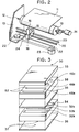
- Fig. 2 shows essential portions of an ink jet printer to which an ink jet print head 15 according to the embodiment of the present invention is mounted.
- a platen 10 for feeding a sheet 11 is rotatably mounted to a frame 13 by a shaft 12.
- a motor 14 is provided for driving the platen 10.
- Two guide rods 20 are also mounted to the frame 13 in parallel to the axis of the platen 10.
- a carriage 18 is slidably supported on the two guide rods 20.
- An ink jet print head 15 and an ink supplier 16 are mounted on the carriage 18 so as to face the platen 10.
- a timing belt 24 wound on a pair of pulleys 22 is fixed to the carriage 18.
- a motor 23 is provided for rotating one of the pulleys 22. Feed of the timing belt 24 moves the carriage 18 in alignment with the platen 10.
- Fig. 3 is an exploded perspective view showing an array 30 used in the ink jet print head 15.
- the array 30 includes a base plate 33 made from a metal or a ceramic with a high modulus of elasticity, a layered-type piezoelectric element 38 according to the present invention, a thin-film vibration plate 35, a channel main body 34, and an orifice plate 36 formed with orifices 37. These components of the array 30 are attached together in the configuration shown in Fig. 3. That is, the base plate 33 is secured on one side of the layered-type piezoelectric element 38 and the thin-film vibration plate 35 is disposed to the other side of the layered-type piezoelectric element 38.
- the layered-type piezoelectric element 38 is attached, via the thin-film vibration plate 35, to one side of the channel main body 34 and the orifice plate 36 is attached to the other of the channel main body 34.
- the channel main body 34 and the orifice plate 36 are formed by injection molding of a resin material.
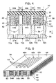
- the layered-type piezoelectric element 38 has formed therein a plurality of slit-shaped elongated holes 52 defining therebetween actuator portions 46a, 46b, and 46c.
- the channel main body 34 has formed therein ink channels 32a, 32b, and 32c extending in parallel with and at positions corresponding to the actuator portions 46a, 46b, and 46c.
- the ink channels 32a, 32b, and 32c are formed longer in the lengthwise direction and wider in the widthwise direction than corresponding actuator portions 46a, 46b, and 46c of the layered-type piezoelectric element 38.
- the array 30 of the present embodiment includes three ejection devices 70a, 70b, 70c, which include the actuator portions 46a, 46b, and 46c and the ink channels 32a, 32b, and 32c respectively.
- the actuator portions 46a, 46b, and 46c of the layered-type piezoelectric element 38 are positioned at cavities formed by the ink channels 32a, 32b, and 32c (which extend perpendicular to the sheet surface of Fig. 4) so that the layered-type piezoelectric element 38 serves as a piezoelectric actuator for the three ejection devices 70a, 70b, and 70c.
- the layered-type piezoelectric element 38 is a multilayered stacked body including: piezoelectric ceramic layers 40 having piezoelectric and electrostrictive properties; internal negative electrode layers 42; and internal positive electrode layers 44a, 44b, and 44c.
- the piezoelectric ceramic layers 40 are composed of a lead zirconium titanate (PZT) ceramic material with ferroelectric properties. As indicated by arrows at the actuator portions 46a, 46b, and 46c in Fig. 4, the piezoelectric ceramic layers 40 are polarized in the direction in which they are stacked.
- the internal negative electrode layers 42 and internal positive electrode layers 44a, 44b, and 44c are composed of a silver-palladium (Ag-Pd) metal material.
- the actuator portions 46a, 46b, and 46c are formed at the central portion of the layered-type piezoelectric element 38 and are divided by the plurality of elongated holes 52.
- the layered-type piezoelectric element 38 includes a piezoelectric inactive portion 48 at an edge portion thereof. The piezoelectric inactive portion 48 connects end portions of the actuator portions 46a, 46b, and 46c together.
- the internal positive electrode layers 44a, 44b, and 44c are divided by the elongated holes 52 to a one-to-one correspondence with the ink channels 32a, 32b, and 32c.
- the internal electrode layers 42, and 44a, 44b, and 44c overlap at overlapping regions 46a 1 (indicated by dotted lines in Fig. 6), 46b 1 , and 46c 1 , that is, at all areas between the elongated holes except the tips of each actuator portion 46a, 46b, and 46c.
- internal electrode layers 42, and 44a, 44b, and 44c do not overlap at the piezoelectric inactive portion 48 nor at non-overlapping regions 46a 2 (indicated by dotted lines in Fig. 6), 46b 2 , and 46c 2 , that is, at the tips of each actuator portion 46a, 46b, and 46c.
- the layered-type piezoelectric element 38 can be produced by the following method.
- a powder of a piezoelectric material which is primarily PZT, is mixed to a desired composition. Then the powder is calcined at 850°C. Next, a defoaming agent, a minute quantity of a plastic material, and five parts by weight binder are added to the powder. The resultant mixture is dispersed in an organic solvent to produce a slurry.
- the slurry is formed into green sheet base plates with a predetermined thickness using a doctor blade. Window-shaped elongated holes 52 are punched into each of the base plates to predetermined dimensions.
- palladium (Pd) paste is then screen printed on the base plates to form green sheets 50 and 51 with the two different patterns of internal electrodes shown in Fig. 6. That is, internal positive electrode layers 44a, 44b, and 44c, whose number is a one-to-one correspondence with the number of the ink channels 32a, 32b, and 32c, are first formed by screen printing on the upper surface of each of one group of base plates. Then, electrode terminal portions 45a, 45b, and 45c of respective internal positive electrode layers 44a, 44b, and 44c are formed on the same base plates by screen printing to produce a group of green sheets 50. On the upper surface of the remainder of the base plates, an internal negative electrode layer 42 with electrode terminal portions 43 is formed traversing across all the ink channels 32a, 32b, and 32c by screen printing to produce green sheets 51.
- the internal electrode layers 42, and 44a, 44b, and 44c are provided with their tip end portions drawn slightly back from the ends of the elongated holes 52 in the lengthwise direction of the elongated holes 52 to insure that, when the green sheets 50, 51 are stacked, the internal positive electrode layers 44 and the internal negative electrode layers 42 overlap each other in the stacked direction only at the overlapping regions 46a 1 , 46b 1 , and 46c 1 . Further, the electrode terminals 43, 45a, 45b, and 45c are formed so as to be exposed on corresponding side edges of the green sheets 50, 51.
- both types of green sheets 50, 51 are stacked alternately to a total of 10 sheets.
- a green sheet (not shown) with no internal electrode layer on the upper surface of its piezoelectric ceramic layer 40.
- the sheets are then heat-pressed into an integrated body. After degreasing, sintering is carried out at approximately 1,200°C, resulting in a stacked body made from piezoelectric elements.
- outer negative electrodes 53 and outer positive electrodes 54a, 54b, 54c are attached to locations where the electrode terminal portions 43, 45a, 45b, and 45c are exposed in the thus-formed stacked body
- a well-known polarization process is executed to polarize the stacked body by application of an electric field.
- the polarization process can be carried out, for example, by immersing the stacked body into an oil bath (not shown) filled with an electrically insulating oil, such as silicon oil, heated to about 130°C.
- An electric field of approximately 2.5 kV/mm is then applied between the outer negative electrodes 53 and the outer positive electrodes 54a, 54b, and 54c to polarize the stacked body.
- the piezoelectric ceramic layers 40 of the stacked body are sufficiently thin, for example, approximately 50 ⁇ m, they can be easily polarized without providing a special environment such as the oil bath. In this case, a voltage of approximately 30 V is applied between the outer negative electrodes 53 and the outer positive electrodes 54a, 54b, and 54c after the ink jet print head 15 has been assembled.
- the layered-type piezoelectric element 38 shown in Fig. 5 can be obtained using the above-described method.
- the elongated holes 52 can be formed simply by a cutting or punching out process. It should be noted that the process described above for making the layered-type piezoelectric element 38 can be performed without any punching processes.
- a green sheet base plate having elongated holes 52 with predetermined dimensions can be produced by performing injection molding techniques using molding materials made from piezoelectric material. None of the above-described methods, that is, whether the elongated holes 52 are formed by a punching out, cutting process, or by injection molding, require any special processing equipment or production processes. Therefore, production can be easily managed and these methods are well suited for mass production techniques.
- the internal electrode layers 42, 44 and the electrode terminal portions 43, 45 may be formed on base plates before punching out or otherwise forming the elongated holes 52.
- the internal positive electrode layers 44a, 44b, and 44c need not be printed so that they are electrically isolated from each other. Instead, the conductive material need only be printed on the base plates so that opening the elongated holes 52 will divide the resultant layer of conductive material into an electrically isolated plurality of internal positive electrode layers 44a, 44b, and 44c whose number corresponds to the number of electrode terminal portions 45a, 45b, and 45c.
- the material of the internal positive electrode layers 44a, 44b, and 44c can therefore be printed using a simpler process.
- green sheets 50 and green sheets 51 are stacked alternately, heat-pressed into an integrated body, degreased, and then sintered. Then, the outer electrodes 53, 54 are formed and the stacked body polarized to produce the layered-type piezoelectric element 38.
- elongated holes can be opened in green sheets after they are stacked together.
- green sheet base plates are molded to the predetermined thickness using a doctor blade or similar device.
- internal negative electrode layers 42 and electrode terminal portions 43 are formed on one group of green sheet base plates.
- Internal positive electrode layers 44 and electrode terminal portions 45 are then formed on another group of green sheet base plates.
- both types of green sheets are stacked alternately to a total of 10 sheets.
- Another green sheet (not shown), which will form a piezoelectric ceramic layer 40 with no internal electrode layer on its upper surface is stacked on top.
- the stack of green sheets are then heat-pressed into an integrated stacked body.
- Elongated holes are then formed at a predetermined pitch in the integrated stacked body by using a punching process.
- the stacked body with elongated holes opened therein undergoes degreasing and sintering.
- the layered-type piezoelectric element 38 is produced by attaching the outer electrodes 53, 54 and polarizing the stacked body.
- This method also eliminates the need to screen print the internal positive electrode layers 44a, 44b, and 44c so that they are electrically isolated from each other.
- the material of the internal positive electrode layers 44a, 44b, and 44c can be printed by a simple process so that forming the elongated holes 52 will divide the resultant layer of conductive material into an electrically isolated plurality of internal positive electrode layers 44a, 44b, and 44c, whose number corresponds to the number of electrode terminal portions 45a, 45b, and 45c.
- the elongated holes are formed after the green sheets are assembled into a stacked and integrated body.
- a stacked body can be produced with edges of the actuator portions 46a, 46b, and 46c properly aligned even if the green sheets are shifted slightly out of alignment.
- the elongated holes 52 should not be opened in an integrated stacked body containing the ultimately desired number of stacked green sheets. Instead, thin integrated stacked bodies are first formed by stacking and heat pressing a few green sheets having the internal electrode layers and other components. Then elongated holes 52 are formed in each of the resultant thin integrated bodies to produce a plurality of thin stacked bodies with elongated holes 52 formed therein. Next, a number of the thin stacked bodies are stacked to obtain a thicker stacked body with the ultimately desired number of stacked layers. Afterward, the resultant thick stacked body is heat-pressed again into an integrated body and then degreased and sintered.
- All of the layered-type piezoelectric elements 38 formed through the above-described methodes have actuator portions 46a, 46b, and 46c connected by their end portions to the piezoelectric non-active region 48. Therefore, even if the actuator portions 46a, 46b, and 46c are thin, they will be supported by the piezoelectric non-active region 48 and so will not break or be damaged during production.
- Electric circuits provided in the array 30 are shown in Fig. 7.
- the outer positive electrodes 54a, 54b, and 54c of the layered-type piezoelectric element 38 are connected to the positive electrode of a drive power source 60 through openable and closable switches 62a, 62b, 62c.
- the outer negative electrodes 53 of the layered-type piezoelectric element 38 and the negative electrode of the drive power source 60 are grounded.
- a controller (not shown) opens and closes the switches 62a, 62b, and 62c to selectively apply a driving voltage from the drive power source 60 between the internal negative electrode layers 42 and the internal positive electrode layers 44 located on a selected one of the actuator portions 46a, 46b, or 46c.
- the controller closes, for example, the switch 62a so that a voltage is applied between the internal negative electrode layers 42 and internal positive electrode layers 44a of the actuator portion 46a, resulting in a bias electric field developing in the piezoelectric ceramic layers 40 between these internal electrode layers.
- Dimensional distortion caused by piezoelectric and electrostrictive longitudinal-effects lengthen the actuator portion 46a in the vertical direction of Fig. 7, thereby reducing the volume in the ink channel 32a.
- An increase in pressure accompanying this volume change ejects ink in the ink channel 32a from the orifice 37a as a droplet 39.
- the switch 62a is opened and the application of voltage is cut off, returning the actuator portion to its original form.
- ink is refilled into the ink channel 32a from the ink supply device 16 via a separate valve (not shown).
- a separate valve not shown
- displacement of the actuator portion 46b will occur so that ink will be ejected from the ink channel 32b.
- the piezoelectric ceramic layers 40 are polarized in the direction in which they are stacked, a large amount of deformation develops in the stacked direction, resulting in highly reliable ink ejection.
- a single layered-type piezoelectric element 38 serves as piezoelectric actuators for all the ejection devices 70a, 70b, and 70c. Therefore, a plurality of arrays 30 assembled together can provide an ink jet print head 15 with a simple configuration that can be produced using simple methods. Therefore, the number and complexity of manufacturing processes can be reduced so that production costs can be reduced.
- the piezoelectric actuators are layered-type piezoelectric elements 38 and because the ink channels 32a, 32b, and 32c are formed longer in the lengthwise direction than corresponding actuator portions 46a, 46b, and 46c, consequently, the actuator portions 46a, 46b, and 46c can effectively and easily deform into corresponding ink channels 32a, 32b, and 32c so that driving voltage can be significantly reduced.
- the internal electrode layers 42, 44 of the layered-type piezoelectric element 38 are formed by screen printing, the electrodes can be simply formed even when the actuator portions 46a, 46b, and 46c and the elongated holes 52 are formed extremely thin. Therefore, an array 30 including the ejection devices 70a, 70b, and 70c can be formed to a small size so that a print head that allows high resolution and a wide printing range can be achieved.
- each of the actuator portions 46a, 46b, and 46c divided by the elongated holes 52 are supported connected together at their end portions by the piezoelectric non-active region 48. Consequently, even when the actuator portions 46a, 46b, and 46c are formed to a narrow width, they will not break or be damaged during production of the print head. Therefore, yield when producing the print head is improved. The actuator portions 46a, 46b, and 46c will also not break when driven, thereby improving reliability of the resultant print head. Also, if the actuator portions 46a, 46b, and 46c can be formed thinner, they can be formed into a more highly integrated unit, which improves print quality of the resultant ink jet print head.
- the electrode terminal portions 43, 45 of the internal negative electrode layers 42 and internal positive electrode layers 44 of the layered-type piezoelectric element 38 according to the present embodiment are exposed to the exterior. Therefore, deterioration of insulating properties, such as deterioration caused by silver migration, is eliminated. Further, advantages such as superior durability and moisture resistance are gained. Also, because the outer negative electrodes 53 and the outer positive electrodes 54a, 54b, and 54c connected to the internal electrode layers 42, 44a, 44b, and 44c are formed on the same side surface of the layered-type piezoelectric element 38, the electrodes can be easily picked up and collectively electrically connected to a drive control circuit or a circuit substrate for controlling drive of the print head. Also, the outer negative electrodes 53 and the outer positive electrodes 54a, 54b, and 54c can be connected to the electric circuit at a single side surface of the array 30 so that less space is taken up.
- one layered-type piezoelectric element 38 serves as piezoelectric actuators for the three ejection devices 70a, 70b, and 70c.
- piezoelectric actuators for additional ejection devices can be formed by adding to, or changing the pattern of, the internal positive electrode layers 44.
- the internal positive electrode layers 44 are divided in a one-to-one correspondence to the ink channels 32a, 32b, and 32c.
- the internal negative electrode layers 42 may be divided to a one-to-one correspondence to the ink channels 32a, 32b, and 32c.
- both the internal positive electrode layers 44 and the internal negative electrode layers 42 may be separated in a one-to-one correspondence to the ink channels 32a, 32b, and 32c. That is, it is sufficient for at least one of the internal electrode layers, either positive or negative, to be divided in a one-to-one correspondence to the ink channels 32a, 32b, and 32c.
- the array 30 can be provided with more or less than the three ink channels described in the present embodiment.
Abstract
Description
- The present invention relates to a layered-type piezoelectric element provided in an ink jet print head which ejects ink droplets to produce diagrams or characters by dots on a print medium and to a method for producing the layered-type piezoelectric element.
- Conventionally, there has been known an ink jet print head including piezoelectric elements. Each piezoelectric element either forms or is attached to a wall surface defining an ink reservoir or ink channel. When one of the piezoelectric elements is applied with a voltage, the piezoelectric element deforms, causing a displacement which changes the volume of the corresponding ink channel. Increase in pressure accompanying the volume change ejects an ink droplet from a nozzle fluidly connected with the ink channel.
- Japanese Patent Application (Kokai) No. HEI-6-79871 discloses a configuration typical for such an ink jet print head. As shown in Fig. 1, vertically-displacing pillar-shaped piezoelectric
ceramic elements 81 serving as layered-type actuators are formed from a block-shaped cintered body into which elongated grooves have been opened with a slicer or other instrument. The piezoelectricceramic elements 81 are configured from stacks of thin piezoelectric element sheets alternating with thin internal electrodes. This configuration allows low voltage drive of the piezoelectricceramic elements 81. The internal electrodes are exposed in alternation at opposing side surfaces of the piezoelectricceramic elements 81. The internal electrodes are connected, by wire bonding or by other means, to a drive power source for supplying a voltage for driving the piezoelectricceramic elements 81. - An elastic
thin plate 82 is adhered to the tip ends of the pillar-shaped piezoelectricceramic elements 81. Further, anozzle plate 84 made from resin and formed withink channels 83 andnozzles 83a is adhered to thethin plate 82 so that tip ends of the piezoelectricceramic elements 81 are positioned overcorresponding ink channels 83. Application of a voltage to the piezoelectricceramic elements 81 produces displacement which deforms thethin plate 82 and ejects ink in theink channel 83 from thenozzles 83a. Dot-pattern characters and other images can therefore be printed. - However, the pillar-shaped piezoelectric
ceramic elements 81 of the ink jet print head shown in Fig. 7 easily break because they are thin independent units. Because the pillar-shaped piezoelectricceramic elements 81 break easily, production yield of the ink jet print head is low. Also, the ink jet print head is unreliable because the pillar-shaped piezoelectricceramic elements 81 can easily break when driven. - Also, producing the piezoelectric
ceramic elements 81 requires many production processes such as machining the pillar-shaped piezoelectric element using a slicer and such as wire bonding for the power supply. The great number of production processes makes the piezoelectricceramic elements 81 expensive to produce. - The object of the present invention is to solve the above-described problems and to provide a reliable and inexpensive way to produce layered-type piezoelectric elements used in an ink jet print head and to provide a high yield method for producing the layered-type piezoelectric element.
- To achieve the above-described objectives, a layered-type piezoelectric element according to one aspect of the present invention is for producing a pressure fluctuation within a cavity of an ink jet print head to eject the ink from the cavity. The layered-type piezoelectric element comprises: piezoelectric ceramic layers; and internal electrode layers stacked in a stacked direction alternately with the piezoelectric ceramic layers to form a stacked body, the internal electrode layers including an odd-numbered electrode layer group and an even-numbered electrode layer group; wherein elongated holes are opened through at least a central portion of the stacked body in the stacked direction, the elongated holes defining a plurality of actuator portions in the stacked body, portions of each layer of the odd-numbered electrode layer group being in opposition in the stacked direction with portions of each layer of the even-numbered electrode layer group at least at the actuator portions of the stacked body.
- Also, at least one group of the odd-numbered electrode layer group and the even-numbered electrode layer group includes a plurality of electrically isolated electrodes disposed at positions corresponding to the actuator portions.
- According to another aspect of the present invention, a method for making a layered-type piezoelectric element for producing a pressure fluctuation within a cavity of an ink jet print head to eject ink from the cavity includes the following steps in the order named: producing from a piezoelectric material a plurality of first and second plate sheets each having elongated holes at a predetermined pitch; forming a first electrode on each of the first plate sheets so that a terminal of each of the first electrodes is exposed on an edge of its corresponding first plate sheet; forming a second electrode on each of the second plate sheets so that a plurality of terminals of each of the second electrodes are exposed on an edge of its corresponding second plate sheet; stacking the first and second sheets in alternation to form a stacked body; and attaching the first and second sheets together by pressing them together.
- According to a further aspect of the present invention, a method for making a layered-type piezoelectric element for producing a pressure fluctuation within a cavity of an ink jet print head to eject the ink from the cavity includes the following steps in the order named: forming a first electrode on each of a group of first plate sheets made from piezoelectric material, each first electrode being formed so that a terminal thereof is exposed on an edge of its corresponding first plate sheet; forming a second electrode on each of a group of second plate sheets made from piezoelectric material, each second electrode being formed so that a plurality of terminals thereof are exposed on an edge of its corresponding second plate sheet; forming elongated holes to a predetermined pitch on each of the first and second plate sheets; stacking the first and second plate sheets in alternation to form a stacked body; and pressing the stacked body to attach the first and second plate sheets together.
- According to a further aspect of the present invention, a method for making a layered-type piezoelectric element for producing a pressure fluctuation within a cavity of an ink jet print head to eject ink from the cavity, includes the following steps in the order named: forming a first electrode on each of a group of first plate sheets made from piezoelectric material, each first electrode being formed so that a terminal thereof is exposed on an edge of its corresponding first plate sheet; forming a second electrode on each of a group of second plate sheets made from piezoelectric material, each second electrode being formed so that a plurality of terminals thereof are exposed on an edge of its corresponding second plate sheet; stacking the first and second plates sheets to form a stacked body; pressing the stacked body to attach the first and second plates sheets together; and forming elongated holes through the stacked body in a stacked direction in which the plate sheets are stacked and at a predetermined pitch in a direction normal to the stacked direction.
- According to a further aspect of the present invention, a print head array comprises: a nozzle plate formed with nozzles; an ink channel plate attached to the nozzle plate, the ink channel plate formed with ink channels having a predetermined size, the ink channels aligned with the nozzles; and a stacked body for producing a pressure fluctuation in the ink channels to eject ink from the nozzles, the stacked body including: piezoelectric ceramic layers; and internal electrode layers stacked in a stacked direction alternately with the piezoelectric ceramic layers, the internal electrode layers including an odd-numbered electrode layer group and an even-numbered electrode layer group; wherein the stacked body is formed through at least a central portion thereof with elongated holes opened in the stacked direction, the elongated holes defining a plurality of actuator portions for producing the pressure fluctuation in the ink chambers, the actuator portions being aligned with the ink chambers and having a predetermined size smaller than the predetermined size of the ink chambers, portions of each layer of the odd-numbered electrode layer group being in opposition in the stacked direction with portions of each layer of the even-numbered electrode layer group at least at the actuator portions of the stacked body, at least one group of the odd-numbered electrode layer group and the even-numbered electrode layer group including a plurality of electrically isolated electrodes disposed at positions corresponding to the actuator portions.
- The above and other objects, features and advantages of the invention will become more apparent from reading the following description of the preferred embodiment taken in connection with the accompanying drawings in which:
- Fig. 1 is a sectional perspective view showing a conventional ink jet print head;
- Fig. 2 is a perspective view showing essential portions of an ink jet printer incorporating an ink jet print head according to the present invention;
- Fig. 3 is an exploded view showing an array of the ink jet print head;
- Fig. 4 is a sectional cross-sectional view showing the array;
- Fig. 5 is a perspective view showing a layered-type piezoelectric element according to the present invention;
- Fig. 6 is an exploded view of the layered-type piezoelectric element; and
- Fig. 7 is perspective view showing electric circuits provided for driving the array.
- A layered-type piezoelectric element and a method of producing the layered-type piezoelectric element according to a preferred embodiment of the present invention will be described while referring to the accompanying drawings wherein like parts and components are designated by the same reference numerals to avoid duplicating description.
- Fig. 2 shows essential portions of an ink jet printer to which an ink
jet print head 15 according to the embodiment of the present invention is mounted. Aplaten 10 for feeding asheet 11 is rotatably mounted to aframe 13 by ashaft 12. Amotor 14 is provided for driving theplaten 10. Twoguide rods 20 are also mounted to theframe 13 in parallel to the axis of theplaten 10. Acarriage 18 is slidably supported on the twoguide rods 20. An inkjet print head 15 and anink supplier 16 are mounted on thecarriage 18 so as to face theplaten 10. Atiming belt 24 wound on a pair ofpulleys 22 is fixed to thecarriage 18. Amotor 23 is provided for rotating one of thepulleys 22. Feed of thetiming belt 24 moves thecarriage 18 in alignment with theplaten 10. - Fig. 3 is an exploded perspective view showing an
array 30 used in the inkjet print head 15. Thearray 30 includes abase plate 33 made from a metal or a ceramic with a high modulus of elasticity, a layered-typepiezoelectric element 38 according to the present invention, a thin-film vibration plate 35, a channelmain body 34, and anorifice plate 36 formed withorifices 37. These components of thearray 30 are attached together in the configuration shown in Fig. 3. That is, thebase plate 33 is secured on one side of the layered-typepiezoelectric element 38 and the thin-film vibration plate 35 is disposed to the other side of the layered-typepiezoelectric element 38. The layered-typepiezoelectric element 38 is attached, via the thin-film vibration plate 35, to one side of the channelmain body 34 and theorifice plate 36 is attached to the other of the channelmain body 34. The channelmain body 34 and theorifice plate 36 are formed by injection molding of a resin material. - The layered-type
piezoelectric element 38 has formed therein a plurality of slit-shapedelongated holes 52 definingtherebetween actuator portions main body 34 has formed thereinink channels actuator portions ink channels corresponding actuator portions piezoelectric element 38. - As can be seen in Fig. 4, the
array 30 of the present embodiment includes threeejection devices actuator portions ink channels actuator portions piezoelectric element 38 are positioned at cavities formed by theink channels piezoelectric element 38 serves as a piezoelectric actuator for the threeejection devices - The layered-type
piezoelectric element 38 is a multilayered stacked body including: piezoelectricceramic layers 40 having piezoelectric and electrostrictive properties; internalnegative electrode layers 42; and internalpositive electrode layers ceramic layers 40 are composed of a lead zirconium titanate (PZT) ceramic material with ferroelectric properties. As indicated by arrows at theactuator portions ceramic layers 40 are polarized in the direction in which they are stacked. The internalnegative electrode layers 42 and internalpositive electrode layers - As can be seen in Fig. 5, the
actuator portions type piezoelectric element 38 and are divided by the plurality ofelongated holes 52. In addition to theactuator portions type piezoelectric element 38 includes a piezoelectricinactive portion 48 at an edge portion thereof. The piezoelectricinactive portion 48 connects end portions of theactuator portions - As shown in Fig. 6, the internal
positive electrode layers elongated holes 52 to a one-to-one correspondence with theink channels regions 46a1 (indicated by dotted lines in Fig. 6), 46b1, and 46c1, that is, at all areas between the elongated holes except the tips of eachactuator portion inactive portion 48 nor atnon-overlapping regions 46a2 (indicated by dotted lines in Fig. 6), 46b2, and 46c2, that is, at the tips of eachactuator portion - The layered-
type piezoelectric element 38 can be produced by the following method. A powder of a piezoelectric material, which is primarily PZT, is mixed to a desired composition. Then the powder is calcined at 850°C. Next, a defoaming agent, a minute quantity of a plastic material, and five parts by weight binder are added to the powder. The resultant mixture is dispersed in an organic solvent to produce a slurry. The slurry is formed into green sheet base plates with a predetermined thickness using a doctor blade. Window-shapedelongated holes 52 are punched into each of the base plates to predetermined dimensions. - Next, palladium (Pd) paste is then screen printed on the base plates to form
green sheets positive electrode layers ink channels terminal portions positive electrode layers green sheets 50. On the upper surface of the remainder of the base plates, an internalnegative electrode layer 42 withelectrode terminal portions 43 is formed traversing across all theink channels green sheets 51. - It should be noted that the internal electrode layers 42, and 44a, 44b, and 44c are provided with their tip end portions drawn slightly back from the ends of the
elongated holes 52 in the lengthwise direction of theelongated holes 52 to insure that, when thegreen sheets regions electrode terminals green sheets - Next, both types of
green sheets ceramic layer 40. The sheets are then heat-pressed into an integrated body. After degreasing, sintering is carried out at approximately 1,200°C, resulting in a stacked body made from piezoelectric elements. As shown in Fig. 5, outernegative electrodes 53 and outerpositive electrodes electrode terminal portions - Then, a well-known polarization process is executed to polarize the stacked body by application of an electric field. The polarization process can be carried out, for example, by immersing the stacked body into an oil bath (not shown) filled with an electrically insulating oil, such as silicon oil, heated to about 130°C. An electric field of approximately 2.5 kV/mm is then applied between the outer
negative electrodes 53 and the outerpositive electrodes ceramic layers 40 of the stacked body are sufficiently thin, for example, approximately 50 µm, they can be easily polarized without providing a special environment such as the oil bath. In this case, a voltage of approximately 30 V is applied between the outernegative electrodes 53 and the outerpositive electrodes jet print head 15 has been assembled. - The layered-
type piezoelectric element 38 shown in Fig. 5 can be obtained using the above-described method. Theelongated holes 52 can be formed simply by a cutting or punching out process. It should be noted that the process described above for making the layered-type piezoelectric element 38 can be performed without any punching processes. For example, a green sheet base plate having elongatedholes 52 with predetermined dimensions can be produced by performing injection molding techniques using molding materials made from piezoelectric material. None of the above-described methods, that is, whether theelongated holes 52 are formed by a punching out, cutting process, or by injection molding, require any special processing equipment or production processes. Therefore, production can be easily managed and these methods are well suited for mass production techniques. - As a variation of the method for producing the layered-type
piezoelectric elements 38, the internal electrode layers 42, 44 and theelectrode terminal portions 43, 45 may be formed on base plates before punching out or otherwise forming the elongated holes 52. In this case, the internalpositive electrode layers elongated holes 52 will divide the resultant layer of conductive material into an electrically isolated plurality of internalpositive electrode layers electrode terminal portions positive electrode layers green sheets 50 andgreen sheets 51 are stacked alternately, heat-pressed into an integrated body, degreased, and then sintered. Then, theouter electrodes 53, 54 are formed and the stacked body polarized to produce the layered-type piezoelectric element 38. - In still another variation of the method for making the layered-
type piezoelectric element 38, elongated holes can be opened in green sheets after they are stacked together. In this case, first, green sheet base plates are molded to the predetermined thickness using a doctor blade or similar device. Then, without punchingelongated holes 52 into the green sheet plates, internal negative electrode layers 42 andelectrode terminal portions 43 are formed on one group of green sheet base plates. Internal positive electrode layers 44 and electrode terminal portions 45 are then formed on another group of green sheet base plates. Next, both types of green sheets are stacked alternately to a total of 10 sheets. Another green sheet (not shown), which will form a piezoelectricceramic layer 40 with no internal electrode layer on its upper surface is stacked on top. The stack of green sheets are then heat-pressed into an integrated stacked body. Elongated holes are then formed at a predetermined pitch in the integrated stacked body by using a punching process. Next, as in the above-described embodiment, the stacked body with elongated holes opened therein undergoes degreasing and sintering. The layered-type piezoelectric element 38 is produced by attaching theouter electrodes 53, 54 and polarizing the stacked body. - This method also eliminates the need to screen print the internal
positive electrode layers positive electrode layers elongated holes 52 will divide the resultant layer of conductive material into an electrically isolated plurality of internalpositive electrode layers electrode terminal portions elongated holes 52 when stacking thegreen sheets actuator portions - Further, in a slight variation to this last process, if the stacked body is thick, whether because it includes many layers of layered-type
piezoelectric elements 38 or for some other reason, then theelongated holes 52 should not be opened in an integrated stacked body containing the ultimately desired number of stacked green sheets. Instead, thin integrated stacked bodies are first formed by stacking and heat pressing a few green sheets having the internal electrode layers and other components. Thenelongated holes 52 are formed in each of the resultant thin integrated bodies to produce a plurality of thin stacked bodies withelongated holes 52 formed therein. Next, a number of the thin stacked bodies are stacked to obtain a thicker stacked body with the ultimately desired number of stacked layers. Afterward, the resultant thick stacked body is heat-pressed again into an integrated body and then degreased and sintered. - All of the layered-type
piezoelectric elements 38 formed through the above-described methodes have actuatorportions non-active region 48. Therefore, even if theactuator portions non-active region 48 and so will not break or be damaged during production. - Electric circuits provided in the
array 30 are shown in Fig. 7. The outerpositive electrodes type piezoelectric element 38 are connected to the positive electrode of adrive power source 60 through openable andclosable switches negative electrodes 53 of the layered-type piezoelectric element 38 and the negative electrode of thedrive power source 60 are grounded. A controller (not shown) opens and closes theswitches drive power source 60 between the internal negative electrode layers 42 and the internal positive electrode layers 44 located on a selected one of theactuator portions - Next, the operation of an ink
jet print head 15 having the above-described configuration will be described. For convenience of explanation, it will be assumed that thearray 30 according to the present embodiment is provided with three ink channels. - In accordance with predetermined print data, the controller closes, for example, the
switch 62a so that a voltage is applied between the internal negative electrode layers 42 and internalpositive electrode layers 44a of theactuator portion 46a, resulting in a bias electric field developing in the piezoelectricceramic layers 40 between these internal electrode layers. Dimensional distortion caused by piezoelectric and electrostrictive longitudinal-effects lengthen theactuator portion 46a in the vertical direction of Fig. 7, thereby reducing the volume in theink channel 32a. An increase in pressure accompanying this volume change ejects ink in theink channel 32a from theorifice 37a as adroplet 39. Following this, theswitch 62a is opened and the application of voltage is cut off, returning the actuator portion to its original form. As theink channel 32a increases in volume, ink is refilled into theink channel 32a from theink supply device 16 via a separate valve (not shown). To give a further example, if anotherswitch 62b is closed, displacement of theactuator portion 46b will occur so that ink will be ejected from theink channel 32b. Because the piezoelectricceramic layers 40 are polarized in the direction in which they are stacked, a large amount of deformation develops in the stacked direction, resulting in highly reliable ink ejection. - Next will be described deformation undergone by the layered-
type piezoelectric element 38 in anarray direction 31 when a voltage is applied thereto. When a voltage of 25 V is applied to, for example,actuator portion 46a, then theoverlapping region 46a1 undergoes a significant displacement of 200 nm or more. On the other hand, the piezoelectricinactive section 48 hardly undergoes displacement at all. Further, displacement at theoverlapping region 46a1 pulls thenon-overlapping regions 46a2, creating some displacement there also. Because theink channels actuator portions actuator portion 46a can efficiently deform intocorresponding ink channel 32a. Consequently,droplet 39 can be effectively ejected using a low driving voltage of only 30 V. - In the piezoelectric-type
ink jet printer 15 of the present embodiment, a single layered-type piezoelectric element 38 serves as piezoelectric actuators for all theejection devices arrays 30 assembled together can provide an inkjet print head 15 with a simple configuration that can be produced using simple methods. Therefore, the number and complexity of manufacturing processes can be reduced so that production costs can be reduced. In addition, because the piezoelectric actuators are layered-typepiezoelectric elements 38 and because theink channels actuator portions actuator portions corresponding ink channels - Further, because the internal electrode layers 42, 44 of the layered-
type piezoelectric element 38 are formed by screen printing, the electrodes can be simply formed even when theactuator portions elongated holes 52 are formed extremely thin. Therefore, anarray 30 including theejection devices - Further, each of the
actuator portions elongated holes 52 are supported connected together at their end portions by the piezoelectricnon-active region 48. Consequently, even when theactuator portions actuator portions actuator portions - Still further, only the
electrode terminal portions 43, 45 of the internal negative electrode layers 42 and internal positive electrode layers 44 of the layered-type piezoelectric element 38 according to the present embodiment are exposed to the exterior. Therefore, deterioration of insulating properties, such as deterioration caused by silver migration, is eliminated. Further, advantages such as superior durability and moisture resistance are gained. Also, because the outernegative electrodes 53 and the outerpositive electrodes type piezoelectric element 38, the electrodes can be easily picked up and collectively electrically connected to a drive control circuit or a circuit substrate for controlling drive of the print head. Also, the outernegative electrodes 53 and the outerpositive electrodes array 30 so that less space is taken up. - While the invention has been described in detail with reference to specific embodiments thereof, it would be apparent to those skilled in the art that various changes and modifications may be made therein without departing from the spirit of the invention, the scope of which is defined by the attached claims.
- For example, in the above-described embodiments, one layered-
type piezoelectric element 38 serves as piezoelectric actuators for the threeejection devices - Further, in the above embodiment, the internal positive electrode layers 44 are divided in a one-to-one correspondence to the
ink channels ink channels ink channels ink channels - Also, the
array 30 can be provided with more or less than the three ink channels described in the present embodiment.
Claims (15)
- A layered-type piezoelectric element for producing a pressure fluctuation within a cavity of an ink jet print head to eject the ink from the cavity, the layered-type piezoelectric element comprising:piezoelectric ceramic layers; andinternal electrode layers stacked in a stacking direction alternately with said piezoelectric ceramic layers to form a stacked body, the internal electrode layers including an odd-numbered electrode layer group and an even-numbered electrode layer group;wherein elongated holes are provided through at least a central portion of the stacked body in the stacked direction, the elongated holes defining therebetween a plurality of actuator portions in the stacked body, portions of each layer of the odd-numbered electrode layer group being stacked above portions of each layer of the even-numbered electrode layer group at least at the actuator portions of the stacked body.
- A layered-type piezoelectric element as claimed in claim 1, wherein at least one group of the odd-numbered electrode layer group and the even-numbered electrode layer group includes a plurality of electrically isolated electrodes disposed at positions corresponding to the actuator portions.
- A layered-type piezoelectric element as claimed in claim 1 or 2, wherein the piezoelectric ceramic layers are polarized in a direction of an electric field produced by application of a voltage between electrode layers.
- A layered-type piezoelectric element as claimed in claim 1, 2 or 3, wherein each electrode layer has a terminal portion, all of the terminal portions being exposed on a same side surface of the stacked body.
- A method for making a layered-type piezoelectric element for producing a pressure fluctuation within a cavity of an ink jet print head to eject ink from the cavity, the method including the steps of producing a plurality of first and second plate sheets of piezoelectric material, with a first electrode on each of the first plate sheets with edge terminals therefor and with a second electrode on each of the second plate sheets and also with edge terminals therefor;stacking the first and second sheets alternately and forming a body thereof, and the manufacturing including steps whereby elongate holes are provided through at least a central portion of the body in the direction of stacking.
- A method according to claim 5, including the following steps in the order named:producing from a piezoelectric material said plurality of first and second plate sheets each having elongated holes at a predetermined pitch;forming a said first electrode on each of the first plate sheets so that a terminal of each of the first electrodes is exposed on an edge of its corresponding first plate sheet;forming a said second electrode on each of the second plate sheets so that a plurality of terminals of each of the second electrodes are exposed on an edge of its corresponding second plate sheet; and, after stacking the first and second sheets in alternation to form a stacked body, attaching the first and second sheets together by pressing them together.
- A method for making a layered-type piezoelectric element as claimed in claim 6, wherein said steps of forming the first and second plate sheets includes:producing green sheets by forming a slurry of piezoelectric material to a predetermined thickness using a coating technique.
- A method for making a layered-type piezoelectric element as claimed in claim 6, wherein said step of producing the plate sheets includes injection molding.
- A method according to claim 5, including the following steps in the order named:forming the first electrodes on each of a group of first plate sheets made from piezoelectric material, each first electrode being formed so that a terminal thereof is exposed on an edge of its corresponding first plate sheet;forming the second electrodes on each of a group of second plate sheets made from piezoelectric material, each second electrode being formed so that a plurality of terminals thereof are exposed on an edge of its corresponding second plate sheet;forming elongated holes to a predetermined pitch in each of the first and second plate sheets; and, after stacking the first and second plate sheets in alternation to form a stacked body, pressing the stacked body to attach the first and second plate sheets together.
- A method according to claim 5, including the following steps in the order named:forming the first electrodes on each of a group of first plate sheets made from piezoelectric material, each first electrode being formed so that a terminal thereof is exposed on an edge of its corresponding first plate sheet;forming the second electrodes on each of a group of second plate sheets made from piezoelectric material, each second electrode being formed so that a plurality of terminals thereof are exposed on an edge of its corresponding second plate sheet;stacking the first and second plate sheets to form a stacked body; and, after pressing the stacked body to attach the first and second plates sheets together, forming elongated holes through the stacked body in the stacking direction and at a predetermined pitch in a direction normal to the stacked direction.
- A method for making a layered-type piezoelectric element as claimed in any of claims 5 to 10, wherein said step of stacking the first and second sheets in alternation includes the step of aligning the terminals of the first and second electrodes to a single surface of the stacked body.
- A method for making a layered-type piezoelectric element as claimed in any of claims 5 to 11, wherein said step of forming the electrodes includes screen printing with a conductive paste.
- A method for making a layered-type piezoelectric element as claimed in any of claims 5 to 12, wherein said step of forming the elongated holes includes punching out or cutting out the elongated holes.
- A method for making a layered-type piezoelectric element as claimed in any of claims 5 to 14, further comprising steps of:producing a plurality of stacked bodies with elongated holes formed therein;stacking the plurality of stacked bodies to form a larger stacked body; andpressing the larger stacked body to attach the plurality of stacked bodies together.
- A print head array comprising:a nozzle plate formed with nozzles;an ink channel plate attached to said nozzle plate, said ink channel plate formed with ink channels having a predetermined size, the ink channels aligned with the nozzles; anda stacked body for producing a pressure fluctuation in the ink channels to eject ink from the nozzles, the stacked body including:piezoelectric ceramic layers; andinternal electrode layers stacked in a stacking direction alternately with said piezoelectric ceramic layers, the internal electrode layers including an odd-numbered electrode layer group and an even-numbered electrode layer group;wherein said stacked body is formed through at least a central portion thereof with elongated holes opened in the stacked direction, the elongated holes defining therebetween a plurality of actuator portions for producing the pressure fluctuation in the ink chambers, the actuator portions being aligned with the ink chambers and having a predetermined size smaller than the predetermined size of the ink chambers, portions of each layer of the odd-numbered electrode layer group being stacked above portions of each layer of the even-numbered electrode layer group at least at the actuator portions of the stacked body, at least one group of the odd-numbered electrode layer group and the even-numbered electrode layer group including a plurality of electrically isolated electrodes disposed at positions corresponding to the actuator portions.
Applications Claiming Priority (2)
| Application Number | Priority Date | Filing Date | Title |
|---|---|---|---|
| JP3090/95 | 1995-01-12 | ||
| JP7003090A JPH08187848A (en) | 1995-01-12 | 1995-01-12 | Laminated type piezoelectric element and its manufacture |
Publications (3)
| Publication Number | Publication Date |
|---|---|
| EP0721839A2 true EP0721839A2 (en) | 1996-07-17 |
| EP0721839A3 EP0721839A3 (en) | 1996-11-20 |
| EP0721839B1 EP0721839B1 (en) | 1999-03-10 |
Family
ID=11547655
Family Applications (1)
| Application Number | Title | Priority Date | Filing Date |
|---|---|---|---|
| EP95309526A Expired - Lifetime EP0721839B1 (en) | 1995-01-12 | 1995-12-29 | Layered-type piezoelectric element and method for producing the layered-type piezoelectric element |
Country Status (4)
| Country | Link |
|---|---|
| US (1) | US5912526A (en) |
| EP (1) | EP0721839B1 (en) |
| JP (1) | JPH08187848A (en) |
| DE (1) | DE69508220T2 (en) |
Cited By (10)
| Publication number | Priority date | Publication date | Assignee | Title |
|---|---|---|---|---|
| EP0819524A1 (en) * | 1996-07-18 | 1998-01-21 | Océ-Technologies B.V. | Ink jet nozzle head with backing member |
| EP0819526A1 (en) * | 1996-07-18 | 1998-01-21 | Océ-Technologies B.V. | Ink jet nozzle head with backing member |
| DE19747178A1 (en) * | 1996-12-26 | 1998-07-02 | Fujitsu Ltd | Ink jet head for printer, facsimile, word processor, copier |
| EP1022141A1 (en) * | 1999-01-25 | 2000-07-26 | Océ-Technologies B.V. | Ink jet array |
| WO2003038495A2 (en) * | 2001-10-22 | 2003-05-08 | Siemens Aktiengesellschaft | Displacement device for a number of objects, method for production of the displacement device and device for splicing a number of optical waveguides |
| EP1336495A1 (en) * | 2002-02-19 | 2003-08-20 | Brother Kogyo Kabushiki Kaisha | Ink-jet head and ink-jet printer |
| EP1338419A1 (en) * | 2002-02-20 | 2003-08-27 | Brother Kogyo Kabushiki Kaisha | Ink-jet head and ink-jet printer |
| EP1364793A1 (en) * | 2001-03-01 | 2003-11-26 | Ngk Insulators, Ltd. | Comb piezoelectric actuator, and its manufacturing method |
| US6953241B2 (en) | 2001-11-30 | 2005-10-11 | Brother Kogyo Kabushiki Kaisha | Ink-jet head having passage unit and actuator units attached to the passage unit, and ink-jet printer having the ink-jet head |
| US7290865B2 (en) | 2002-02-19 | 2007-11-06 | Brother Kogyo Kabushiki Kaisha | Inkjet head |
Families Citing this family (27)
| Publication number | Priority date | Publication date | Assignee | Title |
|---|---|---|---|---|
| DE19646511C1 (en) * | 1996-11-12 | 1998-05-14 | Marco Systemanalyse Entw | Piezo actuator drive or adjustment element |
| US6494566B1 (en) * | 1997-01-31 | 2002-12-17 | Kyocera Corporation | Head member having ultrafine grooves and a method of manufacture thereof |
| JP3058143B2 (en) * | 1998-02-12 | 2000-07-04 | 日本電気株式会社 | Piezoelectric actuator and method of manufacturing the same |
| JPH11240155A (en) * | 1998-02-26 | 1999-09-07 | Fujitsu Ltd | Ink-jet head with protecting layer provided at junction face of nozzle plate and manufacture thereof |
| US6417600B2 (en) | 1998-09-17 | 2002-07-09 | Seiko Epson Corporation | Piezoelectric vibrator unit, method for manufacturing the same, and ink jet recording head comprising the same |
| JP3716724B2 (en) * | 1999-09-30 | 2005-11-16 | ブラザー工業株式会社 | Piezoelectric actuator for piezoelectric ink jet printer head and method for manufacturing the same |
| US7164221B1 (en) * | 1999-10-01 | 2007-01-16 | Ngk Insulators, Ltd. | Piezoelectric/electrostrictive device and method of manufacturing same |
| US6915547B2 (en) | 1999-10-01 | 2005-07-12 | Ngk Insulators, Ltd. | Piezoelectric/electrostrictive device and method of manufacturing same |
| US6586889B1 (en) | 2000-06-21 | 2003-07-01 | Si Diamond Technology, Inc. | MEMS field emission device |
| US7248444B1 (en) * | 2000-07-21 | 2007-07-24 | Lauer Mark A | Electromagnetic heads, flexures, gimbals and actuators formed on and from a wafer substrate |
| JP3956607B2 (en) * | 2000-10-26 | 2007-08-08 | ブラザー工業株式会社 | Piezoelectric inkjet printer head and method for manufacturing piezoelectric inkjet printer head |
| US6699018B2 (en) * | 2001-04-06 | 2004-03-02 | Ngk Insulators, Ltd. | Cell driving type micropump member and method for manufacturing the same |
| JP3873729B2 (en) * | 2001-03-29 | 2007-01-24 | ブラザー工業株式会社 | Piezoelectric actuator, droplet ejecting apparatus, and manufacturing method thereof |
| JP4042442B2 (en) * | 2001-03-29 | 2008-02-06 | ブラザー工業株式会社 | Piezoelectric transducer and droplet ejection device |
| JP4304881B2 (en) * | 2001-05-18 | 2009-07-29 | リコープリンティングシステムズ株式会社 | Inkjet print head |
| JP3852308B2 (en) * | 2001-07-09 | 2006-11-29 | 株式会社村田製作所 | Multilayer piezoelectric element, manufacturing method thereof, and piezoelectric actuator |
| US6505917B1 (en) | 2001-07-13 | 2003-01-14 | Illinois Tool Works Inc. | Electrode patterns for piezo-electric ink jet printer |
| JP3852309B2 (en) * | 2001-07-24 | 2006-11-29 | 株式会社村田製作所 | Multilayer piezoelectric element, manufacturing method thereof, and piezoelectric actuator |
| US6807030B1 (en) | 2001-12-18 | 2004-10-19 | Western Digital (Fremont), Inc. | Enclosed piezoelectric microactuators coupled between head and suspension |
| US6961221B1 (en) | 2001-12-18 | 2005-11-01 | Western Digital (Fremont), Inc. | Piezoelectric microactuators with substantially fixed axis of rotation and magnified stroke |
| US6601948B1 (en) | 2002-01-18 | 2003-08-05 | Illinois Tool Works, Inc. | Fluid ejecting device with drop volume modulation capabilities |
| DE60316486T2 (en) * | 2002-02-19 | 2008-01-17 | Brother Kogyo K.K., Nagoya | Method of making an ink jet printhead |
| JP3693115B2 (en) * | 2002-05-13 | 2005-09-07 | セイコーエプソン株式会社 | Actuator device, liquid jet head, and inspection method thereof |
| JP2004114558A (en) * | 2002-09-27 | 2004-04-15 | Brother Ind Ltd | Inkjet printer head and manufacturing method therefor |
| JP4580745B2 (en) | 2004-12-08 | 2010-11-17 | 株式会社東芝 | Piezoelectric drive MEMS device |
| US7478898B2 (en) * | 2004-12-20 | 2009-01-20 | Ricoh Printing Systems, Ltd. | Recording head for inkjet recording device |
| JP4594262B2 (en) * | 2006-03-17 | 2010-12-08 | 日本碍子株式会社 | Dispensing device |
Citations (5)
| Publication number | Priority date | Publication date | Assignee | Title |
|---|---|---|---|---|
| EP0402171A2 (en) * | 1989-06-09 | 1990-12-12 | Sharp Kabushiki Kaisha | Head for ink-jet printer |
| EP0516188A1 (en) * | 1990-02-23 | 1992-12-02 | Seiko Epson Corporation | Drop-on-demand ink-jet printing head |
| JPH0679871A (en) * | 1993-07-19 | 1994-03-22 | Seiko Epson Corp | Ink-jet head and manufacture thereof |
| EP0616891A1 (en) * | 1993-03-01 | 1994-09-28 | Seiko Epson Corporation | Ink jet recording apparatus and method of controlling same |
| EP0630748A2 (en) * | 1993-05-12 | 1994-12-28 | Seiko Epson Corporation | Ink jet recording head |
Family Cites Families (11)
| Publication number | Priority date | Publication date | Assignee | Title |
|---|---|---|---|---|
| DE2527647C3 (en) * | 1975-06-20 | 1981-06-25 | Siemens AG, 1000 Berlin und 8000 München | Writing implement that works with liquid droplets |
| DE3114192A1 (en) * | 1981-04-08 | 1982-10-28 | Siemens AG, 1000 Berlin und 8000 München | WRITING DEVICE WORKING WITH LIQUID DROPS |
| US4362407A (en) * | 1981-09-08 | 1982-12-07 | Piezo Electric Products, Inc. | Piezoelectric printer and piezoelectric multilam actuator used therein |
| JPS6116867A (en) * | 1984-05-29 | 1986-01-24 | Yasuhiko Ogawa | Pectinate piezoelectric driving device |
| US4766671A (en) * | 1985-10-29 | 1988-08-30 | Nec Corporation | Method of manufacturing ceramic electronic device |
| JP2965602B2 (en) * | 1990-02-26 | 1999-10-18 | 日立金属株式会社 | Stacked displacement element |
| US5402159A (en) * | 1990-03-26 | 1995-03-28 | Brother Kogyo Kabushiki Kaisha | Piezoelectric ink jet printer using laminated piezoelectric actuator |
| US5245244A (en) * | 1991-03-19 | 1993-09-14 | Brother Kogyo Kabushiki Kaisha | Piezoelectric ink droplet ejecting device |
| US5227813A (en) * | 1991-08-16 | 1993-07-13 | Compaq Computer Corporation | Sidewall actuator for a high density ink jet printhead |
| JPH09507804A (en) * | 1994-11-14 | 1997-08-12 | フィリップス エレクトロニクス ネムローゼ フェンノートシャップ | Inkjet recording apparatus and inkjet recording head |
| JPH08252920A (en) * | 1995-03-16 | 1996-10-01 | Brother Ind Ltd | Production of laminated type piezoelectric element |
-
1995
- 1995-01-12 JP JP7003090A patent/JPH08187848A/en active Pending
- 1995-12-27 US US08/579,159 patent/US5912526A/en not_active Expired - Lifetime
- 1995-12-29 EP EP95309526A patent/EP0721839B1/en not_active Expired - Lifetime
- 1995-12-29 DE DE69508220T patent/DE69508220T2/en not_active Expired - Lifetime
Patent Citations (5)
| Publication number | Priority date | Publication date | Assignee | Title |
|---|---|---|---|---|
| EP0402171A2 (en) * | 1989-06-09 | 1990-12-12 | Sharp Kabushiki Kaisha | Head for ink-jet printer |
| EP0516188A1 (en) * | 1990-02-23 | 1992-12-02 | Seiko Epson Corporation | Drop-on-demand ink-jet printing head |
| EP0616891A1 (en) * | 1993-03-01 | 1994-09-28 | Seiko Epson Corporation | Ink jet recording apparatus and method of controlling same |
| EP0630748A2 (en) * | 1993-05-12 | 1994-12-28 | Seiko Epson Corporation | Ink jet recording head |
| JPH0679871A (en) * | 1993-07-19 | 1994-03-22 | Seiko Epson Corp | Ink-jet head and manufacture thereof |
Non-Patent Citations (1)
| Title |
|---|
| PATENT ABSTRACTS OF JAPAN vol. 018, no. 335 (M-1627), 24 June 1994 & JP-A-06 079871 (SEIKO EPSON CORP), 22 March 1994, * |
Cited By (28)
| Publication number | Priority date | Publication date | Assignee | Title |
|---|---|---|---|---|
| EP0819526A1 (en) * | 1996-07-18 | 1998-01-21 | Océ-Technologies B.V. | Ink jet nozzle head with backing member |
| US6161925A (en) * | 1996-07-18 | 2000-12-19 | Oce' Technologies B.V. | Ink jet nozzle head with backing member |
| EP0819524A1 (en) * | 1996-07-18 | 1998-01-21 | Océ-Technologies B.V. | Ink jet nozzle head with backing member |
| DE19747178A1 (en) * | 1996-12-26 | 1998-07-02 | Fujitsu Ltd | Ink jet head for printer, facsimile, word processor, copier |
| DE19747178C2 (en) * | 1996-12-26 | 2000-03-02 | Fujitsu Ltd | Piezoelectric drive ink jet head and method of manufacturing the same |
| EP1022141A1 (en) * | 1999-01-25 | 2000-07-26 | Océ-Technologies B.V. | Ink jet array |
| NL1011128C2 (en) * | 1999-01-25 | 2000-07-27 | Oce Tech Bv | Ink delivery device. |
| US6290347B1 (en) | 1999-01-25 | 2001-09-18 | Oce-Technologies B.V. | Ink jet array |
| EP1364793A4 (en) * | 2001-03-01 | 2007-06-06 | Ngk Insulators Ltd | Comb piezoelectric actuator, and its manufacturing method |
| EP1364793A1 (en) * | 2001-03-01 | 2003-11-26 | Ngk Insulators, Ltd. | Comb piezoelectric actuator, and its manufacturing method |
| WO2003038495A3 (en) * | 2001-10-22 | 2004-04-01 | Siemens Ag | Displacement device for a number of objects, method for production of the displacement device and device for splicing a number of optical waveguides |
| WO2003038495A2 (en) * | 2001-10-22 | 2003-05-08 | Siemens Aktiengesellschaft | Displacement device for a number of objects, method for production of the displacement device and device for splicing a number of optical waveguides |
| US8684496B2 (en) | 2001-11-30 | 2014-04-01 | Brother Kogyo Kabushiki Kaisha | Ink-jet head having passage unit and actuator units attached to the passage unit, and ink-jet printer having the ink-jet head |
| US9114616B2 (en) | 2001-11-30 | 2015-08-25 | Brother Kogyo Kabushiki Kaisha | Ink-jet head having passage unit and actuator units attached to the passage unit, and ink-jet printer having the ink-jet head |
| US11305536B2 (en) | 2001-11-30 | 2022-04-19 | Brother Kogyo Kabushiki Kaisha | Ink-jet head having passage unit and actuator units attached to the passage unit, and ink-jet printer having the ink-jet head |
| US10821730B2 (en) | 2001-11-30 | 2020-11-03 | Brother Kogyo Kabushiki Kaisha | Ink-jet head having passage unit and actuator units attached to the passage unit, and ink-jet printer having the ink-jet head |
| US10357968B2 (en) | 2001-11-30 | 2019-07-23 | Brother Kogyo Kabushiki Kaisha | Ink-jet head having passage unit and actuator units attached to the passage unit, and ink-jet printer having the ink-jet head |
| US7891781B2 (en) | 2001-11-30 | 2011-02-22 | Brother Kogyo Kabushiki Kaisha | Ink-jet head having passage unit and actuator units attached to the passage unit, and ink-jet printer having the ink-jet head |
| US8025369B2 (en) | 2001-11-30 | 2011-09-27 | Brother Kogyo Kabushiki Kaisha | Ink-jet head and ink-jet printer having ink-jet head |
| US8118402B2 (en) | 2001-11-30 | 2012-02-21 | Brother Kogyo Kabushiki Kaisha | Ink-jet head having passage unit and actuator units attached to the passage unit, and ink-jet printer having the ink-jet head |
| US8393711B2 (en) | 2001-11-30 | 2013-03-12 | Brother Kogyo Kabushiki Kaisha | Ink-jet head having passage unit and actuator units attached to the passage unit, and ink-jet printer having the ink-jet head |
| US9925774B2 (en) | 2001-11-30 | 2018-03-27 | Brother Kogyo Kabushiki Kaisha | Ink-jet head having passage unit and actuator units attached to the passage unit, and ink-jet printer having the ink-jet head |
| US6953241B2 (en) | 2001-11-30 | 2005-10-11 | Brother Kogyo Kabushiki Kaisha | Ink-jet head having passage unit and actuator units attached to the passage unit, and ink-jet printer having the ink-jet head |
| US9718271B2 (en) | 2001-11-30 | 2017-08-01 | Brother Kogyo Kabushiki Kaisha | Ink-jet head having passage unit and actuator units attached to the passage unit, and ink-jet printer having the ink-jet head |
| EP1336495A1 (en) * | 2002-02-19 | 2003-08-20 | Brother Kogyo Kabushiki Kaisha | Ink-jet head and ink-jet printer |
| US7290865B2 (en) | 2002-02-19 | 2007-11-06 | Brother Kogyo Kabushiki Kaisha | Inkjet head |
| US7008048B2 (en) | 2002-02-19 | 2006-03-07 | Brother Kogyo Kabushiki Kaisha | Ink-jet head and ink-jet printer having ink-jet head |
| EP1338419A1 (en) * | 2002-02-20 | 2003-08-27 | Brother Kogyo Kabushiki Kaisha | Ink-jet head and ink-jet printer |
Also Published As
| Publication number | Publication date |
|---|---|
| DE69508220T2 (en) | 1999-09-02 |
| EP0721839B1 (en) | 1999-03-10 |
| JPH08187848A (en) | 1996-07-23 |
| EP0721839A3 (en) | 1996-11-20 |
| US5912526A (en) | 1999-06-15 |
| DE69508220D1 (en) | 1999-04-15 |
Similar Documents
| Publication | Publication Date | Title |
|---|---|---|
| EP0721839B1 (en) | Layered-type piezoelectric element and method for producing the layered-type piezoelectric element | |
| EP0732209B1 (en) | Method for producing a layered piezoelectric element | |
| US5860202A (en) | Method for producing a layered piezoelectric element | |
| JP2913806B2 (en) | Piezoelectric inkjet printer head | |
| US6863383B2 (en) | Piezoelectric transducer and ink ejector using the piezoelectric transducer | |
| JP3716724B2 (en) | Piezoelectric actuator for piezoelectric ink jet printer head and method for manufacturing the same | |
| EP0402171B1 (en) | Head for ink-jet printer | |
| KR100764323B1 (en) | Piezoelectric actuator, method of manufacture, and ink-jet printhead | |
| JP3249545B2 (en) | Piezoelectric inkjet printer head | |
| US6739704B2 (en) | Piezoelectric transducer and ink ejector using piezoelectric transducer | |
| EP1705012B1 (en) | Piezoelectric actuator, liquid transporting apparatus, and method of producing piezoelectric actuator | |
| US5945773A (en) | Piezoelectric actuator for ink-jet printer and method of manufacturing the same | |
| US5818483A (en) | Actuator body structure for a piezoelectric ink ejecting printing apparatus | |
| JP3128857B2 (en) | Piezoelectric inkjet printer head | |
| JP2004096068A (en) | Piezoelectric element, piezoelectric actuator, and liquid injection head | |
| JPH0349957A (en) | Piezoelectric ink jet printer head | |
| JPH06312505A (en) | Laminated type piezoelectric displacement element and ink jet record head using the same | |
| JP2002225269A (en) | Ink-jet printer head and its piezoelectric element | |
| JP3997729B2 (en) | Piezoelectric actuator, inkjet head using the piezoelectric actuator, and manufacturing method thereof | |
| JPH03274159A (en) | Piezoelectric type ink jet printer head | |
| JP3156411B2 (en) | Ink jet print head and method of manufacturing the same | |
| JP3365510B2 (en) | Method of manufacturing ink jet recording head | |
| JP3826587B2 (en) | Inkjet head drive device | |
| JP3266893B2 (en) | Piezoelectric inkjet printer head | |
| JP3873094B2 (en) | Piezoelectric element |
Legal Events
| Date | Code | Title | Description |
|---|---|---|---|
| PUAI | Public reference made under article 153(3) epc to a published international application that has entered the european phase |
Free format text: ORIGINAL CODE: 0009012 |
|
| AK | Designated contracting states |
Kind code of ref document: A2 Designated state(s): DE GB |
|
| PUAL | Search report despatched |
Free format text: ORIGINAL CODE: 0009013 |
|
| AK | Designated contracting states |
Kind code of ref document: A3 Designated state(s): DE GB |
|
| 17P | Request for examination filed |
Effective date: 19970311 |
|
| GRAG | Despatch of communication of intention to grant |
Free format text: ORIGINAL CODE: EPIDOS AGRA |
|
| 17Q | First examination report despatched |
Effective date: 19980331 |
|
| GRAG | Despatch of communication of intention to grant |
Free format text: ORIGINAL CODE: EPIDOS AGRA |
|
| GRAH | Despatch of communication of intention to grant a patent |
Free format text: ORIGINAL CODE: EPIDOS IGRA |
|
| GRAH | Despatch of communication of intention to grant a patent |
Free format text: ORIGINAL CODE: EPIDOS IGRA |
|
| GRAA | (expected) grant |
Free format text: ORIGINAL CODE: 0009210 |
|
| AK | Designated contracting states |
Kind code of ref document: B1 Designated state(s): DE GB |
|
| REF | Corresponds to: |
Ref document number: 69508220 Country of ref document: DE Date of ref document: 19990415 |
|
| PLBE | No opposition filed within time limit |
Free format text: ORIGINAL CODE: 0009261 |
|
| STAA | Information on the status of an ep patent application or granted ep patent |
Free format text: STATUS: NO OPPOSITION FILED WITHIN TIME LIMIT |
|
| 26N | No opposition filed | ||
| REG | Reference to a national code |
Ref country code: GB Ref legal event code: IF02 |
|
| PGFP | Annual fee paid to national office [announced via postgrant information from national office to epo] |
Ref country code: GB Payment date: 20141124 Year of fee payment: 20 |
|
| PGFP | Annual fee paid to national office [announced via postgrant information from national office to epo] |
Ref country code: DE Payment date: 20141222 Year of fee payment: 20 |
|
| REG | Reference to a national code |
Ref country code: DE Ref legal event code: R071 Ref document number: 69508220 Country of ref document: DE |
|
| REG | Reference to a national code |
Ref country code: GB Ref legal event code: PE20 Expiry date: 20151228 |
|
| PG25 | Lapsed in a contracting state [announced via postgrant information from national office to epo] |
Ref country code: GB Free format text: LAPSE BECAUSE OF EXPIRATION OF PROTECTION Effective date: 20151228 |