EP0717357A2 - Disk array apparatus - Google Patents
Disk array apparatus Download PDFInfo
- Publication number
- EP0717357A2 EP0717357A2 EP95309117A EP95309117A EP0717357A2 EP 0717357 A2 EP0717357 A2 EP 0717357A2 EP 95309117 A EP95309117 A EP 95309117A EP 95309117 A EP95309117 A EP 95309117A EP 0717357 A2 EP0717357 A2 EP 0717357A2
- Authority
- EP
- European Patent Office
- Prior art keywords
- parity
- high speed
- data
- disk
- memory
- Prior art date
- Legal status (The legal status is an assumption and is not a legal conclusion. Google has not performed a legal analysis and makes no representation as to the accuracy of the status listed.)
- Granted
Links
- 230000009977 dual effect Effects 0.000 claims abstract description 10
- 238000013500 data storage Methods 0.000 claims description 2
- 238000004364 calculation method Methods 0.000 abstract description 23
- 230000002452 interceptive effect Effects 0.000 abstract description 3
- 230000006870 function Effects 0.000 description 8
- 230000005055 memory storage Effects 0.000 description 7
- 238000003491 array Methods 0.000 description 6
- 238000000034 method Methods 0.000 description 5
- 238000012546 transfer Methods 0.000 description 5
- 238000010586 diagram Methods 0.000 description 3
- 238000007726 management method Methods 0.000 description 3
- 230000008901 benefit Effects 0.000 description 2
- 230000006872 improvement Effects 0.000 description 2
- 238000012545 processing Methods 0.000 description 2
- 230000005540 biological transmission Effects 0.000 description 1
- 230000003139 buffering effect Effects 0.000 description 1
- 238000004891 communication Methods 0.000 description 1
- 238000010276 construction Methods 0.000 description 1
- 238000013461 design Methods 0.000 description 1
- 230000008520 organization Effects 0.000 description 1
- 230000002093 peripheral effect Effects 0.000 description 1
- 230000008569 process Effects 0.000 description 1
- 230000008929 regeneration Effects 0.000 description 1
- 238000011069 regeneration method Methods 0.000 description 1
- 230000000717 retained effect Effects 0.000 description 1
Images
Classifications
-
- G—PHYSICS
- G06—COMPUTING; CALCULATING OR COUNTING
- G06F—ELECTRIC DIGITAL DATA PROCESSING
- G06F11/00—Error detection; Error correction; Monitoring
- G06F11/07—Responding to the occurrence of a fault, e.g. fault tolerance
- G06F11/08—Error detection or correction by redundancy in data representation, e.g. by using checking codes
- G06F11/10—Adding special bits or symbols to the coded information, e.g. parity check, casting out 9's or 11's
- G06F11/1076—Parity data used in redundant arrays of independent storages, e.g. in RAID systems
-
- G—PHYSICS
- G06—COMPUTING; CALCULATING OR COUNTING
- G06F—ELECTRIC DIGITAL DATA PROCESSING
- G06F3/00—Input arrangements for transferring data to be processed into a form capable of being handled by the computer; Output arrangements for transferring data from processing unit to output unit, e.g. interface arrangements
- G06F3/06—Digital input from, or digital output to, record carriers, e.g. RAID, emulated record carriers or networked record carriers
-
- G—PHYSICS
- G11—INFORMATION STORAGE
- G11B—INFORMATION STORAGE BASED ON RELATIVE MOVEMENT BETWEEN RECORD CARRIER AND TRANSDUCER
- G11B20/00—Signal processing not specific to the method of recording or reproducing; Circuits therefor
- G11B20/10—Digital recording or reproducing
- G11B20/18—Error detection or correction; Testing, e.g. of drop-outs
- G11B20/1833—Error detection or correction; Testing, e.g. of drop-outs by adding special lists or symbols to the coded information
Definitions
- the present invention relates to disk array apparatus and in particular, but not exclusively, to a hardware disk array controller providing improved performance, and the execution of concurrent data movements and parity calculations.
- a Redundant Array of Inexpensive Disks referred to as a RAID storage system, is a collection of disk drives which appears as a single large disk drive to a host computer system. Additionally, part of the disk storage capacity is utilized to store redundant information about user data stored on the remainder of the storage capacity. This redundant information allows the disk array to continue to function without the loss of data should an array disk drive member fail, and permits the regeneration of data to a replacement array disk drive member.
- the first level RAID comprises N disks for storing data and N additional "mirror" disks for storing copies of the information written to the data disks.
- RAID level 1 write functions require that data be written to two disks, the second "mirror" disk receiving redundant information, i.e., the same information provided to the first disk. When data is read, it can be read from either disk.
- RAID level 3 systems comprise one or more groups of N+1 disks. Within each group, N disks are used to store data, and the additional disk is utilized to store redundant information, i.e., parity information.
- each block of data is divided into N portions for storage among the N data disks.
- the corresponding parity information is calculated by determining the exclusive-OR product of the data written to the N data disks and written to a dedicated parity disk. When data is read, all N data disks must be accessed. The parity disk is used to reconstruct information in the event of a disk failure.
- a RAID level 2 system is similar to the RAID level 3 systems described above, but includes additional redundant disks for identifying disk drive failures,
- RAID level 4 systems are also comprised of one or more groups of N+1 disks wherein N disks are used to store data, and the additional disk is utilized to store parity information.
- RAID level 4 systems differ from RAID level 3 systems in that data to be saved is divided into larger portions, consisting of one or many blocks of data, for storage among the disks. Write operations still require access to two disks, i.e., one of the N data disks and the parity disk. In a similar fashion, read operations typically need only access a single one of the N data disks, unless the data to be read exceeds the block length stored on each disk.
- the parity disk is used to reconstruct information in the event of a disk failure.
- RAID level 5 is similar to RAID level 4 except that parity information, in addition to the data, is distributed across the N+1 disks in each group. Although each group contains N+1 disks, each disk includes some blocks for storing data and some blocks for storing parity information. The location at which parity information is stored is controlled by an algorithm implemented by the user. As in RAID level 4 systems, RAID level 5 write operations require access to at least two disks. However, no longer does every write operation to a group require access to the same dedicated parity disk, as in RAID level 4 systems. This feature provides the opportunity to perform concurrent write operations.
- parity data in either a RAID level 4 or 5 system can be calculated by performing a bit-wise exclusive-OR of corresponding portions of the data stored across the N data drives.
- RAID level 4 or 5 Although the parity calculation for RAID levels 4 or 5 shown in the above equation is much simpler than performing a bit-wise exclusive-OR of corresponding portions of the data stored across all of the data drives, a typical RAID level 4 or 5 write operation will require a minimum of two disk read and two disk write operations. More than two disk read and write operations are required for data write operations involving more than one data block. Each individual disk read operation involves a seek and rotation to the appropriate disk track and sector to be read. The seek time for all disks is therefore the maximum of the seek times of each disk. A RAID level 4 or 5 system thus carries a significant write penalty when compared with a single disk storage device or with RAID level 1, 2 or 3 systems.
- the present invention seeks to provide for an improved disk array apparatus and also a related method of operating such arrays.
- disk array apparatus for operation with a host computer and a plurality of disk drive means comprising a first high speed local bus, an interface connecting said first high speed local bus with said host computer, at least one interface connecting said plurality of disk drive means with said first high speed local bus and a processor means connected to said first high speed local bus for controlling the operation of the components connected thereto, characterized by parity assist logic means connected to said first high speed local bus, local data means storage, and a second high speed local bus connecting said parity assist logic means with said local storage means wherein said parity assist logic means provide data via said second high speed local bus to said local storage means for the determination of parity data during disk array write operations.
- the present invention advantageously provides a new and useful a disk array controller hardware architecture that improves controller performance.
- the present invention provides a disk array controller architecture which allows concurrent data movements and parity calculations, and the concurrent execution of time independent tasks.
- a disk array controller which includes unique parity assist logic and a dedicated local memory for performing parity generation and data reconstruction operations.
- the present invention advantageously can provide a new and useful disk array controller architecture which permits the simultaneous operation of data block moves between storage I/O devices and a local memory; data block moves between a host system and the local memory; parity calculations; and normal array controller processor memory fetches.
- the invention relates to the disk array control method embodied within the above apparatus.
- a disk array system for storing data received from, and providing stored data to, a host computer system.
- the disk array system includes a first high speed local bus; an interface circuit connecting the first high speed local bus with the host computer system; a plurality of disk drive members; at least one interface circuit connecting the plurality of disk drive members with the first high speed local bus; a parity assist logic circuit connected to the first high speed local bus; a local memory storage; a second high speed local bus connecting the parity assist logic with said local memory storage; and a processor connected to the first high speed local bus for controlling the operation of the components connected to said first high speed local bus.
- the parity assist logic provides data via the second high speed local bus to the local memory required for the calculation of parity data during disk array write operations, and manipulates the data saved to the local memory to determine parity during disk array write operations.
- the invention can also provide a disk array control apparatus for a disk array system including a plurality of disk drive members for storing data received from, and providing stored data to, a host computer system, said disk array controller comprising a first high speed local bus, an interface circuit connecting said first high speed local bus with said host computer system, at least one interface circuit connecting said plurality of disk drive members with said first high speed local bus, a parity assist logic circuit connected to said first high speed local bus, a local memory storage, a second high speed local bus connecting said parity assist logic with said local memory storage, wherein said parity assist logic provides data via said second high speed local bus to said local memory required for the calculation of parity data during disk array write operations, and manipulates the data saved to said local memory to determine parity during said disk array write operations, and a processor connected to said first high speed local bus for controlling the operation of the components connected to said first high speed local bus.
- the parity assist logic includes a parity assist engine, including exclusive-OR logic, for calculating parity; a dual ported memory interface connecting said parity assist engine with said local memory via said second high speed local bus; and an interface circuit connecting said dual ported memory interface with said first high speed local bus.
- the first local bus is a high speed PCI buses.
- the second bus is a dual port memory interface.
- the array controller architecture is scalable and supports RAID modes 0, 3, 4 and 5.
- the architecture features a high bandwidth parity calculation engine and a buffered PCI interface operating at the full speed of the high speed PCI local bus. It features multi processing so that multiple tasks may be queued for execution. Additionally, it provides a way to attach blocks of up to 128 MBytes of additional local RAM memory to the PCI bus.
- the additional local memory is dual ported so that PCI and parity operations may operate concurrently.
- the invention can advantageously provide for a high performance scalable hardware architecture for a disk array storage subsystem which supports RAID modes 0, 3, 4 and 5.
- the architecture features a high bandwidth parity calculation engine, a buffered PCI interface operating at the full speed of a PCI bus, and a dedicated local memory.
- the dedicated local memory is dual ported so that PCI and parity operations may operate concurrently.
- the architecture of the disk array controller allows parity calculations and memory block moves to occur without interfering with the controller processor or its associated memory, freeing the controller processor to manage array task control.
- the array controller configuration allows simultaneous operation of data block moves between storage I/O devices and local memory; data block moves between host SCSI connections and local memory; parity calculations; and normal CPU memory fetches, queued operations for block moves and queued operations for parity tasks.
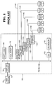
- FIG. 1 A simple block diagram of a known disk array system is shown in Fig. 1.
- the system includes an intelligent array controller 100 for managing the transfer of data between a host computer system 12 and N disk drive units, five of which, identified as DRIVE A through DRIVE E, are shown in Fig. 1.
- Central to the array controller is a high speed local bus 102, such as a Peripheral Component Interconnect (PCI).
- PCI Peripheral Component Interconnect
- a host SCSI interface 104 and SCSI bus 14 provide connection between the host computer system 12 and PCI bus 102.
- PCI Peripheral Component Interconnect
- each of disk drives DRIVE A through DRIVE E are connected to PCI bus 102 through a SCSI drive interface, identified by reference numerals 112A through 112E, respectively, and corresponding SCSI buses 114A through 114E.
- Parity functions are performed by a parity logic circuit 108 and local memory 110, both of which are also connected to the PCI bus 102.
- Communication between, and operation of, the controller components is controlled by a processor 106, in accordance with instructions residing in a processor memory 118.
- the construction and operation of the array controller shown in Fig. 1, as well as the components included in the controller, will be readily understood by those skilled in the art.
- the RAID storage process requires many parity calculations and data movement operations to create the necessary data redundancy, or reconstruct data following a disk failure.
- array controller architecture shown in Fig. 1 and described above, much use of the PCI bus 102 is required to transfer new data, old data, reconstructed data, old parity information and new parity information between the host computer system 12.
- the array drives DRIVE A through DRIVE E, the local memory 110 and the parity logic 106 to generate new parity information during an array write operation or to reconstruct data following an array failure.
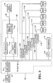
- the disk array system shown in Fig. 2 includes many of the components shown in Fig. 1 and discussed earlier. For those components common to the controller architectures and array systems, the reference numerals of Fig. 1 have been retained in Fig. 2. Common components of the systems shown in Figs. 1 and 2 include: high speed PCI bus 102, host SCSI interface 104, SCSI bus 14, SCSI drive interfaces 112A through 112E, SCSI buses 114A through 114E, disk drive members DRIVE A through DRIVE E, processor 106 and processor memory 118.
- the array controller architecture shown in Fig. 2 improves upon previously known array controller architectures by removing the parity logic and the local memory utilized for parity generation and the reconstruction of data from the PCI bus 102.
- the controller architecture shown in Fig. 2 provides an independent parity assist engine 132 and local memory 136 interconnected through a dual ported memory interface 134.
- a high speed PCI interface 130 provides for the transmission of data between PCI bus 102 and local memory 136.
- the PCI bus interface 130, parity calculation engine 132, and dual ported memory interface 134 are shown integrated together into a single RAID parity assist chip 128. However, these three components operate independently, in a coordinated manner, to provide high speed data storage and parity calculations while using a minimum of host CPU cycles.
- a high speed local bus 138 connects the RAID parity assist chip with the local memory 136.
- data blocks are received from the host SCSI channel 14 and stored in local memory 136.
- the parity assist engine 132 reads the data, calculates the parity information and writes it back to local memory 136.
- the final data blocks are then written to the appropriate disk drives from the local memory 136.
- Disk read operations start with data moved from the disk drives to local memory 136. This data is then transferred to the host SCSI channel 14 unless the parity information is needed to reconstruct the data.
- local memory 136 is organized for high bandwidth operation with a 72 bit wide interface. It also supports interleaved cycles for maximum performance.
- the memory system is capable of operating at the full clock speed of the RAID parity assist chip. Refresh control is also included so that economical dynamic RAM can be used for storage. A powered-down mode of operation is provided to protect the memory data if power fails.
- the PCI interface module 130 is capable of full speed PCI bus transfers. It is designed to respond to all bus modes from single byte to full bandwidth bursts.
- the PCI module contains a 128 byte (First-In First-Out) FIFO register to store data accepted from the PCI bus. This allows the PCI transfer to continue even if local memory is temporarily unavailable.
- the parity assist engine 132 operates on data stored in the local memory 136. It calculates parity a burst at a time utilizing a 128 byte FIFO to store the intermediate results. The intermediate results are not written back to local memory. For maximum performance the control logic for the parity assist engine maintains pointers to each needed data block. The parity engine operates at the full speed of the local memory bus to provide the fastest possible performance for the memory bandwidth.
- the parity assist engine contains 4 separate sections that allow additional tasks to be queued up while one task executes. Each task maintains its own control and status register so that task scheduling does not interfere with the currently executing task.
- the engine can be configured as a single engine which works on wide arrays up to 22+1 drives wide, or as a four engine machine which operates with arrays as wide as 4+1 drives.
- An intermediate mode provides a two engine machine with up to 10+1 drives.
- the parity engine includes exclusive-OR logic providing RAID 5 and RAID 3 parity generation/checking as well as move and zero check modes.
- One of the most important parts of the architecture is the time independent operation it provides. Blocks of data are not required to be accessed simultaneously for parity calculations. Disk operations which span several drives may be scheduled and executed as soon as possible by each device. Unrelated disk operations may continue even though all drive operations for a single task are not yet complete. This independence improves the performance of the slowest part of the system, the disk drive. It also simplifies the software task of managing concurrent hardware resource requirements.
- the invention features time independent data block moves; time independent parity calculations; queued RAID operations (Up to 3 queued tasks); full speed PCI transfer operations (4 bytes/clock cycle); and full speed parity calculations (4 bytes/clock cycle). Furthermore, the architecture is scalable via the addition of additional RAID Parity Assist chips and local memory storage.
- a disk array controller architecture having an independent memory structure for buffering data, and an independent parity calculation engine permitting parallel operation of array tasks. It allows parity calculations and memory block moves to occur without interfering with the CPU or its memory, freeing the CPU to manage array task control.
- the disclosed array controller configuration allows simultaneous operation of data block moves between storage I/O devices and local memory; data block moves between host SCSI connections and local memory; parity calculations; and normal CPU memory fetches, queued operations for block moves and queued operations for parity tasks.
- the invention can provide for a disk array system including a first high speed local bus; an interface circuit connecting said first high speed local bus with said host computer system; a plurality of disk drive members; at least one interface circuit connecting said plurality of disk drive members with said first high speed local bus; and a processor connected to said first high speed local bus for controlling the operation of the components connected to said first high speed local bus; having the improvement comprising a parity assist logic circuit connected to said first high speed local bus; a local memory storage; and a second high speed local bus connecting said parity assist logic with said local memory storage; wherein said parity assist logic provides data via said second high speed local bus to said local memory required for the calculation of parity data during disk array write operations, and manipulates the data saved to said local memory to determine parity during said array write operations.
Abstract
Description
- The present invention relates to disk array apparatus and in particular, but not exclusively, to a hardware disk array controller providing improved performance, and the execution of concurrent data movements and parity calculations.
- A Redundant Array of Inexpensive Disks, referred to as a RAID storage system, is a collection of disk drives which appears as a single large disk drive to a host computer system. Additionally, part of the disk storage capacity is utilized to store redundant information about user data stored on the remainder of the storage capacity. This redundant information allows the disk array to continue to function without the loss of data should an array disk drive member fail, and permits the regeneration of data to a replacement array disk drive member.
- Several RAID disk array design alternatives are presented in an article titled "A Case for Redundant Arrays of Inexpensive Disks (RAID)" by David A. Patterson, Garth Gibson and Randy H. Katz; University of California Report No. UCB/CSD 87/391, December 1987. The article discusses disk arrays and the improvements in performance, reliability, power consumption and scalability that disk arrays provide in comparison to single large magnetic disks.
- Five disk array arrangements are described in the article. The first level RAID comprises N disks for storing data and N additional "mirror" disks for storing copies of the information written to the data disks. RAID level 1 write functions require that data be written to two disks, the second "mirror" disk receiving redundant information, i.e., the same information provided to the first disk. When data is read, it can be read from either disk.
-
RAID level 3 systems comprise one or more groups of N+1 disks. Within each group, N disks are used to store data, and the additional disk is utilized to store redundant information, i.e., parity information. DuringRAID level 3 write functions, each block of data is divided into N portions for storage among the N data disks. The corresponding parity information is calculated by determining the exclusive-OR product of the data written to the N data disks and written to a dedicated parity disk. When data is read, all N data disks must be accessed. The parity disk is used to reconstruct information in the event of a disk failure. - A RAID level 2 system is similar to the
RAID level 3 systems described above, but includes additional redundant disks for identifying disk drive failures, - RAID level 4 systems are also comprised of one or more groups of N+1 disks wherein N disks are used to store data, and the additional disk is utilized to store parity information. RAID level 4 systems differ from
RAID level 3 systems in that data to be saved is divided into larger portions, consisting of one or many blocks of data, for storage among the disks. Write operations still require access to two disks, i.e., one of the N data disks and the parity disk. In a similar fashion, read operations typically need only access a single one of the N data disks, unless the data to be read exceeds the block length stored on each disk. As withRAID level 3 systems, the parity disk is used to reconstruct information in the event of a disk failure. - RAID level 5 is similar to RAID level 4 except that parity information, in addition to the data, is distributed across the N+1 disks in each group. Although each group contains N+1 disks, each disk includes some blocks for storing data and some blocks for storing parity information. The location at which parity information is stored is controlled by an algorithm implemented by the user. As in RAID level 4 systems, RAID level 5 write operations require access to at least two disks. However, no longer does every write operation to a group require access to the same dedicated parity disk, as in RAID level 4 systems. This feature provides the opportunity to perform concurrent write operations.
- As with
RAID level 3, parity data in either a RAID level 4 or 5 system can be calculated by performing a bit-wise exclusive-OR of corresponding portions of the data stored across the N data drives. However, because each parity bit is simply the exclusive-OR product of all the corresponding data bits from the data drives, new parity can be more easily determined from the old data and the old parity as well as the new data in accordance with the following equation:
- Although the parity calculation for RAID levels 4 or 5 shown in the above equation is much simpler than performing a bit-wise exclusive-OR of corresponding portions of the data stored across all of the data drives, a typical RAID level 4 or 5 write operation will require a minimum of two disk read and two disk write operations. More than two disk read and write operations are required for data write operations involving more than one data block. Each individual disk read operation involves a seek and rotation to the appropriate disk track and sector to be read. The seek time for all disks is therefore the maximum of the seek times of each disk. A RAID level 4 or 5 system thus carries a significant write penalty when compared with a single disk storage device or with
RAID level 1, 2 or 3 systems. - In order to coordinate the operation of the disk drives within an array to perform read and write functions, to map received data onto the array disk drive members, generate and check redundant information, and provide data restoration and reconstruction, complex storage management techniques are required. In many early disk array systems, the array management software necessary to perform these complex storage management techniques is executed within the host computer system. The host system thereby functions as the disk array controller and performs the generation and checking of redundant information as well as coordinating the many other storage management operations required of the disk array. Having the host perform these functions is expensive in host processing overhead.
- The present invention seeks to provide for an improved disk array apparatus and also a related method of operating such arrays.
- In accordance with the present invention there is provided disk array apparatus for operation with a host computer and a plurality of disk drive means comprising a first high speed local bus, an interface connecting said first high speed local bus with said host computer, at least one interface connecting said plurality of disk drive means with said first high speed local bus and a processor means connected to said first high speed local bus for controlling the operation of the components connected thereto, characterized by parity assist logic means connected to said first high speed local bus, local data means storage, and a second high speed local bus connecting said parity assist logic means with said local storage means wherein said parity assist logic means provide data via said second high speed local bus to said local storage means for the determination of parity data during disk array write operations.
- The present invention advantageously provides a new and useful a disk array controller hardware architecture that improves controller performance.
- Also, the present invention provides a disk array controller architecture which allows concurrent data movements and parity calculations, and the concurrent execution of time independent tasks.
- It is yet another advantage of the present invention that a disk array controller can be provided which includes unique parity assist logic and a dedicated local memory for performing parity generation and data reconstruction operations.
- Further the present invention advantageously can provide a new and useful disk array controller architecture which permits the simultaneous operation of data block moves between storage I/O devices and a local memory; data block moves between a host system and the local memory; parity calculations; and normal array controller processor memory fetches.
- It is yet another advantage of the present invention that a disk array controller architecture which also permits queued operation of block moves and queued operation for parity tasks can be provided.
- It should also be appreciated that the invention relates to the disk array control method embodied within the above apparatus.
- Preferably there can be provided, in accordance with the present invention, a disk array system for storing data received from, and providing stored data to, a host computer system. The disk array system includes a first high speed local bus; an interface circuit connecting the first high speed local bus with the host computer system; a plurality of disk drive members; at least one interface circuit connecting the plurality of disk drive members with the first high speed local bus; a parity assist logic circuit connected to the first high speed local bus; a local memory storage; a second high speed local bus connecting the parity assist logic with said local memory storage; and a processor connected to the first high speed local bus for controlling the operation of the components connected to said first high speed local bus. The parity assist logic provides data via the second high speed local bus to the local memory required for the calculation of parity data during disk array write operations, and manipulates the data saved to the local memory to determine parity during disk array write operations.
- The invention can also provide a disk array control apparatus for a disk array system including a plurality of disk drive members for storing data received from, and providing stored data to, a host computer system, said disk array controller comprising a first high speed local bus, an interface circuit connecting said first high speed local bus with said host computer system, at least one interface circuit connecting said plurality of disk drive members with said first high speed local bus, a parity assist logic circuit connected to said first high speed local bus, a local memory storage, a second high speed local bus connecting said parity assist logic with said local memory storage, wherein said parity assist logic provides data via said second high speed local bus to said local memory required for the calculation of parity data during disk array write operations, and manipulates the data saved to said local memory to determine parity during said disk array write operations, and a processor connected to said first high speed local bus for controlling the operation of the components connected to said first high speed local bus.
- In the described embodiment, the parity assist logic includes a parity assist engine, including exclusive-OR logic, for calculating parity; a dual ported memory interface connecting said parity assist engine with said local memory via said second high speed local bus; and an interface circuit connecting said dual ported memory interface with said first high speed local bus. The first local bus is a high speed PCI buses. The second bus is a dual port memory interface.
- The array controller architecture is scalable and supports
RAID modes 0, 3, 4 and 5. The architecture features a high bandwidth parity calculation engine and a buffered PCI interface operating at the full speed of the high speed PCI local bus. It features multi processing so that multiple tasks may be queued for execution. Additionally, it provides a way to attach blocks of up to 128 MBytes of additional local RAM memory to the PCI bus. The additional local memory is dual ported so that PCI and parity operations may operate concurrently. - Thus, it should be appreciated that the invention can advantageously provide for a high performance scalable hardware architecture for a disk array storage subsystem which supports
RAID modes 0, 3, 4 and 5. The architecture features a high bandwidth parity calculation engine, a buffered PCI interface operating at the full speed of a PCI bus, and a dedicated local memory. The dedicated local memory is dual ported so that PCI and parity operations may operate concurrently. The architecture of the disk array controller allows parity calculations and memory block moves to occur without interfering with the controller processor or its associated memory, freeing the controller processor to manage array task control. The array controller configuration allows simultaneous operation of data block moves between storage I/O devices and local memory; data block moves between host SCSI connections and local memory; parity calculations; and normal CPU memory fetches, queued operations for block moves and queued operations for parity tasks. - The invention is described further hereinafter by way of example only, with reference to the accompanying drawings in which:
- Fig. 1 is a simple block diagram of a prior art disk array system utilizing a high speed PCI bus; and
- Fig. 2 is a simple block diagram of a disk array system utilizing a high speed PCI bus and a high performance parity function architecture in accordance with an embodiment of the present invention.
- Most disk array systems in use today are self-contained, including a dedicated controller for executing the array management software, thus relieving the host system of these operations. A simple block diagram of a known disk array system is shown in Fig. 1. The system includes an
intelligent array controller 100 for managing the transfer of data between ahost computer system 12 and N disk drive units, five of which, identified as DRIVE A through DRIVE E, are shown in Fig. 1. Central to the array controller is a high speed local bus 102, such as a Peripheral Component Interconnect (PCI). Ahost SCSI interface 104 andSCSI bus 14 provide connection between thehost computer system 12 and PCI bus 102. Similarly, each of disk drives DRIVE A through DRIVE E are connected to PCI bus 102 through a SCSI drive interface, identified byreference numerals 112A through 112E, respectively, andcorresponding SCSI buses 114A through 114E. Parity functions are performed by aparity logic circuit 108 andlocal memory 110, both of which are also connected to the PCI bus 102. Communication between, and operation of, the controller components is controlled by aprocessor 106, in accordance with instructions residing in aprocessor memory 118. The construction and operation of the array controller shown in Fig. 1, as well as the components included in the controller, will be readily understood by those skilled in the art. - The RAID storage process requires many parity calculations and data movement operations to create the necessary data redundancy, or reconstruct data following a disk failure. In the array controller architecture shown in Fig. 1 and described above, much use of the PCI bus 102 is required to transfer new data, old data, reconstructed data, old parity information and new parity information between the
host computer system 12. The array drives DRIVE A through DRIVE E, thelocal memory 110 and theparity logic 106 to generate new parity information during an array write operation or to reconstruct data following an array failure. - The disk array system shown in Fig. 2 includes many of the components shown in Fig. 1 and discussed earlier. For those components common to the controller architectures and array systems, the reference numerals of Fig. 1 have been retained in Fig. 2. Common components of the systems shown in Figs. 1 and 2 include: high speed PCI bus 102,
host SCSI interface 104,SCSI bus 14,SCSI drive interfaces 112A through 112E,SCSI buses 114A through 114E, disk drive members DRIVE A through DRIVE E,processor 106 andprocessor memory 118. - However, the array controller architecture shown in Fig. 2 improves upon previously known array controller architectures by removing the parity logic and the local memory utilized for parity generation and the reconstruction of data from the PCI bus 102. The controller architecture shown in Fig. 2 provides an independent parity assist
engine 132 andlocal memory 136 interconnected through a dual portedmemory interface 134. A highspeed PCI interface 130 provides for the transmission of data between PCI bus 102 andlocal memory 136. - The
PCI bus interface 130,parity calculation engine 132, and dual portedmemory interface 134 are shown integrated together into a single RAID parity assistchip 128. However, these three components operate independently, in a coordinated manner, to provide high speed data storage and parity calculations while using a minimum of host CPU cycles. A high speedlocal bus 138 connects the RAID parity assist chip with thelocal memory 136. - During a disk write operation, data blocks are received from the
host SCSI channel 14 and stored inlocal memory 136. Theparity assist engine 132 reads the data, calculates the parity information and writes it back tolocal memory 136. The final data blocks are then written to the appropriate disk drives from thelocal memory 136. - Disk read operations start with data moved from the disk drives to
local memory 136. This data is then transferred to thehost SCSI channel 14 unless the parity information is needed to reconstruct the data. - Since this architecture is very memory intensive,
local memory 136 is organized for high bandwidth operation with a 72 bit wide interface. It also supports interleaved cycles for maximum performance. The memory system is capable of operating at the full clock speed of the RAID parity assist chip. Refresh control is also included so that economical dynamic RAM can be used for storage. A powered-down mode of operation is provided to protect the memory data if power fails. - The
PCI interface module 130 is capable of full speed PCI bus transfers. It is designed to respond to all bus modes from single byte to full bandwidth bursts. The PCI module contains a 128 byte (First-In First-Out) FIFO register to store data accepted from the PCI bus. This allows the PCI transfer to continue even if local memory is temporarily unavailable. - The
parity assist engine 132 operates on data stored in thelocal memory 136. It calculates parity a burst at a time utilizing a 128 byte FIFO to store the intermediate results. The intermediate results are not written back to local memory. For maximum performance the control logic for the parity assist engine maintains pointers to each needed data block. The parity engine operates at the full speed of the local memory bus to provide the fastest possible performance for the memory bandwidth. - The parity assist engine contains 4 separate sections that allow additional tasks to be queued up while one task executes. Each task maintains its own control and status register so that task scheduling does not interfere with the currently executing task. Several configuration options are provided to tailor the parity engine to the array organization. The engine can be configured as a single engine which works on wide arrays up to 22+1 drives wide, or as a four engine machine which operates with arrays as wide as 4+1 drives. An intermediate mode provides a two engine machine with up to 10+1 drives.
- The parity engine includes exclusive-OR logic providing RAID 5 and
RAID 3 parity generation/checking as well as move and zero check modes. - One of the most important parts of the architecture is the time independent operation it provides. Blocks of data are not required to be accessed simultaneously for parity calculations. Disk operations which span several drives may be scheduled and executed as soon as possible by each device. Unrelated disk operations may continue even though all drive operations for a single task are not yet complete. This independence improves the performance of the slowest part of the system, the disk drive. It also simplifies the software task of managing concurrent hardware resource requirements.
- The invention features time independent data block moves; time independent parity calculations; queued RAID operations (Up to 3 queued tasks); full speed PCI transfer operations (4 bytes/clock cycle); and full speed parity calculations (4 bytes/clock cycle). Furthermore, the architecture is scalable via the addition of additional RAID Parity Assist chips and local memory storage.
- It can thus be seen that there has been provided by the present invention a disk array controller architecture having an independent memory structure for buffering data, and an independent parity calculation engine permitting parallel operation of array tasks. It allows parity calculations and memory block moves to occur without interfering with the CPU or its memory, freeing the CPU to manage array task control. The disclosed array controller configuration allows simultaneous operation of data block moves between storage I/O devices and local memory; data block moves between host SCSI connections and local memory; parity calculations; and normal CPU memory fetches, queued operations for block moves and queued operations for parity tasks.
- It will therefore be appreciated that the invention can provide for a disk array system including a first high speed local bus; an interface circuit connecting said first high speed local bus with said host computer system; a plurality of disk drive members; at least one interface circuit connecting said plurality of disk drive members with said first high speed local bus; and a processor connected to said first high speed local bus for controlling the operation of the components connected to said first high speed local bus; having the improvement comprising a parity assist logic circuit connected to said first high speed local bus; a local memory storage; and a second high speed local bus connecting said parity assist logic with said local memory storage; wherein said parity assist logic provides data via said second high speed local bus to said local memory required for the calculation of parity data during disk array write operations, and manipulates the data saved to said local memory to determine parity during said array write operations.
- The invention is not restricted to the details of the foregoing embodiment and it should be understood that various changes may be made within the scope of the appended claims.
Claims (4)
- Disk array apparatus for operation with a host computer (12) and a plurality of disk drive means (114A-114E) comprising a first high speed local bus (102), an interface (104) connecting said first high speed local bus (102) with said host computer (12), at least one interface (112A-112E) connecting said plurality of disk drive means (114A-114E) with said first high speed local bus (102), and processor means (106) connected to said first high speed local bus (102) for controlling the operation of the components connected to said first high speed local bus, characterized by parity assist logic means (132) connected to said first high speed local bus (102), local data storage means (136), and a second high speed local bus (138) connecting said parity assist logic means (132) with said local storage means (136), wherein said parity assist logic means (132) is arranged to provide data via said second high speed local bus (138) to said local storage means (136) for the determination of parity data during disk array write operations.
- Apparatus as claimed in Claim 1, wherein said parity assist logic means (132) comprises a parity assist engine (132), a dual ported memory interface (134) connecting said parity assist engine (132) with said local storage means (136) via said second high speed local bus (138), and an interface circuit (130) for connecting said dual ported memory interface (134) with said first high speed local bus (102).
- Apparatus as claimed in Claim 2, wherein said parity assist engine (132) comprises an exclusive-OR circuit.
- Apparatus as claimed in any one of Claims 1 to 3, and comprising a disk array controller.
Applications Claiming Priority (2)
| Application Number | Priority Date | Filing Date | Title |
|---|---|---|---|
| US08/357,847 US5634033A (en) | 1994-12-16 | 1994-12-16 | Disk array storage system architecture for parity operations simultaneous with other data operations |
| US357847 | 2003-02-04 |
Publications (3)
| Publication Number | Publication Date |
|---|---|
| EP0717357A2 true EP0717357A2 (en) | 1996-06-19 |
| EP0717357A3 EP0717357A3 (en) | 1997-05-28 |
| EP0717357B1 EP0717357B1 (en) | 2003-02-26 |
Family
ID=23407284
Family Applications (1)
| Application Number | Title | Priority Date | Filing Date |
|---|---|---|---|
| EP95309117A Expired - Lifetime EP0717357B1 (en) | 1994-12-16 | 1995-12-14 | Disk array apparatus |
Country Status (5)
| Country | Link |
|---|---|
| US (1) | US5634033A (en) |
| EP (1) | EP0717357B1 (en) |
| JP (1) | JP3850478B2 (en) |
| KR (1) | KR100351964B1 (en) |
| DE (1) | DE69529728T2 (en) |
Cited By (5)
| Publication number | Priority date | Publication date | Assignee | Title |
|---|---|---|---|---|
| WO1998000789A1 (en) * | 1996-06-28 | 1998-01-08 | Lsi Logic Corporation | Inter-bus bridge circuit |
| US5937174A (en) * | 1996-06-28 | 1999-08-10 | Lsi Logic Corporation | Scalable hierarchial memory structure for high data bandwidth raid applications |
| GB2341715A (en) * | 1998-09-17 | 2000-03-22 | Springtek Limited | Magnetic disk redundant array |
| EP1046981A1 (en) * | 1997-12-17 | 2000-10-25 | Matsushita Electric Industrial Co., Ltd. | Magnetic disk apparatus and method of data transfer |
| EP1255197A2 (en) * | 2001-04-30 | 2002-11-06 | STMicroelectronics, Inc. | System and method for correcting soft errors in random access memory devices |
Families Citing this family (35)
| Publication number | Priority date | Publication date | Assignee | Title |
|---|---|---|---|---|
| CA2220974A1 (en) * | 1995-05-22 | 1996-11-28 | Mti Technology Corporation | Disk array system including a dual-ported staging memory and concurrent redundancy calculation capability |
| US5774641A (en) * | 1995-09-14 | 1998-06-30 | International Business Machines Corporation | Computer storage drive array with command initiation at respective drives |
| JP2981482B2 (en) * | 1995-12-06 | 1999-11-22 | 日本アイ・ビー・エム株式会社 | Data storage system, data transfer method and data reconstruction method |
| US5790773A (en) * | 1995-12-29 | 1998-08-04 | Symbios, Inc. | Method and apparatus for generating snapshot copies for data backup in a raid subsystem |
| US5835694A (en) * | 1996-12-06 | 1998-11-10 | International Business Machines Corporation | Raid-configured disk drive array wherein array control occurs at the disk drive level |
| US6065096A (en) * | 1997-09-30 | 2000-05-16 | Lsi Logic Corporation | Integrated single chip dual mode raid controller |
| US6134630A (en) * | 1997-11-14 | 2000-10-17 | 3Ware | High-performance bus architecture for disk array system |
| US6631477B1 (en) * | 1998-03-13 | 2003-10-07 | Emc Corporation | Host system for mass storage business continuance volumes |
| US6122754A (en) * | 1998-05-22 | 2000-09-19 | International Business Machines Corporation | Method and system for data recovery using a distributed and scalable data structure |
| US6173415B1 (en) | 1998-05-22 | 2001-01-09 | International Business Machines Corporation | System for scalable distributed data structure having scalable availability |
| US6065083A (en) * | 1998-08-21 | 2000-05-16 | International Business Machines, Inc. | Increasing I/O performance through storage of packetized operational information in local memory |
| US6134623A (en) * | 1998-08-21 | 2000-10-17 | International Business Machines Corporation | Method and system for taking advantage of a pre-stage of data between a host processor and a memory system |
| US6425023B1 (en) | 1999-03-24 | 2002-07-23 | International Business Machines Corporation | Method and system for gathering and buffering sequential data for a transaction comprising multiple data access requests |
| US6286074B1 (en) | 1999-03-24 | 2001-09-04 | International Business Machines Corporation | Method and system for reading prefetched data across a bridge system |
| US6449678B1 (en) | 1999-03-24 | 2002-09-10 | International Business Machines Corporation | Method and system for multiple read/write transactions across a bridge system |
| US6502157B1 (en) | 1999-03-24 | 2002-12-31 | International Business Machines Corporation | Method and system for perfetching data in a bridge system |
| US6772108B1 (en) * | 1999-09-22 | 2004-08-03 | Netcell Corp. | Raid controller system and method with ATA emulation host interface |
| US6542945B1 (en) * | 1999-09-28 | 2003-04-01 | Intel Corporation | Instant configuration of a digital device |
| JP2001344076A (en) * | 2000-06-05 | 2001-12-14 | Fujitsu Ltd | Disk array device |
| TW560678U (en) * | 2001-06-15 | 2003-11-01 | Accusys Inc | Floppy disk array device having large storage capacity |
| US20030131167A1 (en) * | 2001-12-20 | 2003-07-10 | Rankin Linda J. | Node ID discovery |
| KR100467102B1 (en) * | 2002-05-28 | 2005-01-24 | (주) 그레이프테크놀로지 | Data storage system |
| US6941408B2 (en) * | 2002-09-30 | 2005-09-06 | Lsi Logic Corporation | Bus interface system with two separate data transfer interfaces |
| US20040068591A1 (en) * | 2002-10-03 | 2004-04-08 | Workman Michael Lee | Systems and methods of multiple access paths to single ported storage devices |
| US20040123027A1 (en) * | 2002-10-03 | 2004-06-24 | Workman Michael Lee | Systems and methods of multiple access paths to single ported storage devices |
| CN1296845C (en) * | 2003-01-24 | 2007-01-24 | 华为技术有限公司 | Magnetic disk storage system |
| US7236987B1 (en) | 2003-02-28 | 2007-06-26 | Sun Microsystems Inc. | Systems and methods for providing a storage virtualization environment |
| US8166128B1 (en) | 2003-02-28 | 2012-04-24 | Oracle America, Inc. | Systems and methods for dynamically updating a virtual volume in a storage virtualization environment |
| US7290168B1 (en) | 2003-02-28 | 2007-10-30 | Sun Microsystems, Inc. | Systems and methods for providing a multi-path network switch system |
| US7383381B1 (en) | 2003-02-28 | 2008-06-03 | Sun Microsystems, Inc. | Systems and methods for configuring a storage virtualization environment |
| JP4426261B2 (en) * | 2003-11-25 | 2010-03-03 | 株式会社日立製作所 | Channel adapter and disk array device |
| US8209551B2 (en) * | 2008-02-15 | 2012-06-26 | Intel Corporation | Security for RAID systems |
| JP2009230608A (en) * | 2008-03-25 | 2009-10-08 | Fuji Xerox Co Ltd | Storage system, control device, image forming apparatus and control program |
| US8756371B2 (en) | 2011-10-12 | 2014-06-17 | Lsi Corporation | Methods and apparatus for improved raid parity computation in a storage controller |
| US9086992B1 (en) | 2012-06-08 | 2015-07-21 | Digital Ordnance Storage, Inc. | System and method for interconnecting storage elements |
Citations (3)
| Publication number | Priority date | Publication date | Assignee | Title |
|---|---|---|---|---|
| EP0369707A2 (en) * | 1988-11-14 | 1990-05-23 | Emc Corporation | Arrayed disk drive system and method |
| US5257391A (en) * | 1991-08-16 | 1993-10-26 | Ncr Corporation | Disk controller having host interface and bus switches for selecting buffer and drive busses respectively based on configuration control signals |
| US5373512A (en) * | 1991-09-13 | 1994-12-13 | International Business Machines Corporation | Memory controller with parity generator for an I/O control unit |
Family Cites Families (10)
| Publication number | Priority date | Publication date | Assignee | Title |
|---|---|---|---|---|
| US5218689A (en) * | 1988-08-16 | 1993-06-08 | Cray Research, Inc. | Single disk emulation interface for an array of asynchronously operating disk drives |
| US5206943A (en) * | 1989-11-03 | 1993-04-27 | Compaq Computer Corporation | Disk array controller with parity capabilities |
| US5263145A (en) * | 1990-05-24 | 1993-11-16 | International Business Machines Corporation | Method and means for accessing DASD arrays with tuned data transfer rate and concurrency |
| US5191584A (en) * | 1991-02-20 | 1993-03-02 | Micropolis Corporation | Mass storage array with efficient parity calculation |
| US5345565A (en) * | 1991-03-13 | 1994-09-06 | Ncr Corporation | Multiple configuration data path architecture for a disk array controller |
| US5398253A (en) * | 1992-03-11 | 1995-03-14 | Emc Corporation | Storage unit generation of redundancy information in a redundant storage array system |
| US5469566A (en) * | 1992-03-12 | 1995-11-21 | Emc Corporation | Flexible parity generation circuit for intermittently generating a parity for a plurality of data channels in a redundant array of storage units |
| US5375217A (en) * | 1992-03-25 | 1994-12-20 | Ncr Corporation | Method and apparatus for synchronizing disk drive requests within a disk array |
| US5418925A (en) * | 1992-10-23 | 1995-05-23 | At&T Global Information Solutions Company | Fast write I/O handling in a disk array using spare drive for buffering |
| US5392244A (en) * | 1993-08-19 | 1995-02-21 | Hewlett-Packard Company | Memory systems with data storage redundancy management |
-
1994
- 1994-12-16 US US08/357,847 patent/US5634033A/en not_active Expired - Lifetime
-
1995
- 1995-12-14 EP EP95309117A patent/EP0717357B1/en not_active Expired - Lifetime
- 1995-12-14 DE DE69529728T patent/DE69529728T2/en not_active Expired - Fee Related
- 1995-12-15 KR KR1019950052615A patent/KR100351964B1/en not_active IP Right Cessation
- 1995-12-18 JP JP32869895A patent/JP3850478B2/en not_active Expired - Lifetime
Patent Citations (3)
| Publication number | Priority date | Publication date | Assignee | Title |
|---|---|---|---|---|
| EP0369707A2 (en) * | 1988-11-14 | 1990-05-23 | Emc Corporation | Arrayed disk drive system and method |
| US5257391A (en) * | 1991-08-16 | 1993-10-26 | Ncr Corporation | Disk controller having host interface and bus switches for selecting buffer and drive busses respectively based on configuration control signals |
| US5373512A (en) * | 1991-09-13 | 1994-12-13 | International Business Machines Corporation | Memory controller with parity generator for an I/O control unit |
Cited By (9)
| Publication number | Priority date | Publication date | Assignee | Title |
|---|---|---|---|---|
| WO1998000789A1 (en) * | 1996-06-28 | 1998-01-08 | Lsi Logic Corporation | Inter-bus bridge circuit |
| US5881254A (en) * | 1996-06-28 | 1999-03-09 | Lsi Logic Corporation | Inter-bus bridge circuit with integrated memory port |
| US5937174A (en) * | 1996-06-28 | 1999-08-10 | Lsi Logic Corporation | Scalable hierarchial memory structure for high data bandwidth raid applications |
| EP1046981A1 (en) * | 1997-12-17 | 2000-10-25 | Matsushita Electric Industrial Co., Ltd. | Magnetic disk apparatus and method of data transfer |
| EP1046981A4 (en) * | 1997-12-17 | 2005-09-07 | Matsushita Electric Ind Co Ltd | Magnetic disk apparatus and method of data transfer |
| GB2341715A (en) * | 1998-09-17 | 2000-03-22 | Springtek Limited | Magnetic disk redundant array |
| EP1255197A2 (en) * | 2001-04-30 | 2002-11-06 | STMicroelectronics, Inc. | System and method for correcting soft errors in random access memory devices |
| EP1255197A3 (en) * | 2001-04-30 | 2004-04-14 | STMicroelectronics, Inc. | System and method for correcting soft errors in random access memory devices |
| US6792567B2 (en) | 2001-04-30 | 2004-09-14 | Stmicroelectronics, Inc. | System and method for correcting soft errors in random access memory devices |
Also Published As
| Publication number | Publication date |
|---|---|
| DE69529728D1 (en) | 2003-04-03 |
| JP3850478B2 (en) | 2006-11-29 |
| EP0717357B1 (en) | 2003-02-26 |
| US5634033A (en) | 1997-05-27 |
| EP0717357A3 (en) | 1997-05-28 |
| DE69529728T2 (en) | 2003-11-20 |
| KR100351964B1 (en) | 2002-12-26 |
| JPH08235754A (en) | 1996-09-13 |
| KR960024859A (en) | 1996-07-20 |
Similar Documents
| Publication | Publication Date | Title |
|---|---|---|
| EP0717357B1 (en) | Disk array apparatus | |
| JP3302688B2 (en) | Logical Track Write Scheduling System for Parallel Disk Drive Array Data Storage Subsystem | |
| US5720027A (en) | Redundant disc computer having targeted data broadcast | |
| US5345565A (en) | Multiple configuration data path architecture for a disk array controller | |
| US5418925A (en) | Fast write I/O handling in a disk array using spare drive for buffering | |
| US5596708A (en) | Method and apparatus for the protection of write data in a disk array | |
| US5959860A (en) | Method and apparatus for operating an array of storage devices | |
| US5598549A (en) | Array storage system for returning an I/O complete signal to a virtual I/O daemon that is separated from software array driver and physical device driver | |
| US5371882A (en) | Spare disk drive replacement scheduling system for a disk drive array data storage subsystem | |
| US5608891A (en) | Recording system having a redundant array of storage devices and having read and write circuits with memory buffers | |
| US6604172B2 (en) | Disk array device with selectable method for generating redundant data | |
| US5487160A (en) | Concurrent image backup for disk storage system | |
| KR100211788B1 (en) | Failure prediction for disk arrays | |
| EP0594464B1 (en) | Method of operating a data storage disk array | |
| US5566316A (en) | Method and apparatus for hierarchical management of data storage elements in an array storage device | |
| US5522065A (en) | Method for performing write operations in a parity fault tolerant disk array | |
| US5867640A (en) | Apparatus and method for improving write-throughput in a redundant array of mass storage devices | |
| EP0572564A4 (en) | ||
| US20050193273A1 (en) | Method, apparatus and program storage device that provide virtual space to handle storage device failures in a storage system | |
| CA2126754A1 (en) | Method for performing disk array operations using a nonuniform stripe size mapping scheme | |
| US5375217A (en) | Method and apparatus for synchronizing disk drive requests within a disk array | |
| KR19980044001A (en) | VRAM-based Parity Engine in Disk Array Controllers | |
| WO1992004674A1 (en) | Computer memory array control | |
| GB2298306A (en) | A disk array and tasking means | |
| JPH0736633A (en) | Magnetic disk array |
Legal Events
| Date | Code | Title | Description |
|---|---|---|---|
| PUAI | Public reference made under article 153(3) epc to a published international application that has entered the european phase |
Free format text: ORIGINAL CODE: 0009012 |
|
| AK | Designated contracting states |
Kind code of ref document: A2 Designated state(s): DE FR GB |
|
| PUAL | Search report despatched |
Free format text: ORIGINAL CODE: 0009013 |
|
| AK | Designated contracting states |
Kind code of ref document: A3 Designated state(s): DE FR GB |
|
| 17P | Request for examination filed |
Effective date: 19970627 |
|
| RAP1 | Party data changed (applicant data changed or rights of an application transferred) |
Owner name: SYMBIOS, INC. |
|
| RAP1 | Party data changed (applicant data changed or rights of an application transferred) |
Owner name: HYUNDAI ELECTRONICS AMERICA |
|
| 17Q | First examination report despatched |
Effective date: 20000821 |
|
| GRAG | Despatch of communication of intention to grant |
Free format text: ORIGINAL CODE: EPIDOS AGRA |
|
| GRAG | Despatch of communication of intention to grant |
Free format text: ORIGINAL CODE: EPIDOS AGRA |
|
| GRAH | Despatch of communication of intention to grant a patent |
Free format text: ORIGINAL CODE: EPIDOS IGRA |
|
| GRAH | Despatch of communication of intention to grant a patent |
Free format text: ORIGINAL CODE: EPIDOS IGRA |
|
| GRAA | (expected) grant |
Free format text: ORIGINAL CODE: 0009210 |
|
| AK | Designated contracting states |
Designated state(s): DE FR GB |
|
| REG | Reference to a national code |
Ref country code: GB Ref legal event code: FG4D |
|
| REF | Corresponds to: |
Ref document number: 69529728 Country of ref document: DE Date of ref document: 20030403 Kind code of ref document: P |
|
| ET | Fr: translation filed | ||
| PLBE | No opposition filed within time limit |
Free format text: ORIGINAL CODE: 0009261 |
|
| STAA | Information on the status of an ep patent application or granted ep patent |
Free format text: STATUS: NO OPPOSITION FILED WITHIN TIME LIMIT |
|
| 26N | No opposition filed |
Effective date: 20031127 |
|
| REG | Reference to a national code |
Ref country code: GB Ref legal event code: 732E |
|
| PGFP | Annual fee paid to national office [announced via postgrant information from national office to epo] |
Ref country code: FR Payment date: 20051208 Year of fee payment: 11 |
|
| PGFP | Annual fee paid to national office [announced via postgrant information from national office to epo] |
Ref country code: DE Payment date: 20051209 Year of fee payment: 11 |
|
| PGFP | Annual fee paid to national office [announced via postgrant information from national office to epo] |
Ref country code: GB Payment date: 20051214 Year of fee payment: 11 |
|
| REG | Reference to a national code |
Ref country code: FR Ref legal event code: TP |
|
| REG | Reference to a national code |
Ref country code: GB Ref legal event code: 732E |
|
| REG | Reference to a national code |
Ref country code: GB Ref legal event code: 732E |
|
| PG25 | Lapsed in a contracting state [announced via postgrant information from national office to epo] |
Ref country code: DE Free format text: LAPSE BECAUSE OF NON-PAYMENT OF DUE FEES Effective date: 20070703 |
|
| GBPC | Gb: european patent ceased through non-payment of renewal fee |
Effective date: 20061214 |
|
| REG | Reference to a national code |
Ref country code: FR Ref legal event code: ST Effective date: 20070831 |
|
| PG25 | Lapsed in a contracting state [announced via postgrant information from national office to epo] |
Ref country code: GB Free format text: LAPSE BECAUSE OF NON-PAYMENT OF DUE FEES Effective date: 20061214 |
|
| PG25 | Lapsed in a contracting state [announced via postgrant information from national office to epo] |
Ref country code: FR Free format text: LAPSE BECAUSE OF NON-PAYMENT OF DUE FEES Effective date: 20070102 |