EP0715409B1 - Circuit for limiting the output voltage of a power transistor - Google Patents
Circuit for limiting the output voltage of a power transistor Download PDFInfo
- Publication number
- EP0715409B1 EP0715409B1 EP94830556A EP94830556A EP0715409B1 EP 0715409 B1 EP0715409 B1 EP 0715409B1 EP 94830556 A EP94830556 A EP 94830556A EP 94830556 A EP94830556 A EP 94830556A EP 0715409 B1 EP0715409 B1 EP 0715409B1
- Authority
- EP
- European Patent Office
- Prior art keywords
- transistor
- terminal
- junction element
- semiconductor junction
- circuit
- Prior art date
- Legal status (The legal status is an assumption and is not a legal conclusion. Google has not performed a legal analysis and makes no representation as to the accuracy of the status listed.)
- Expired - Lifetime
Links
Images

Classifications
-
- H—ELECTRICITY
- H03—ELECTRONIC CIRCUITRY
- H03K—PULSE TECHNIQUE
- H03K17/00—Electronic switching or gating, i.e. not by contact-making and –breaking
- H03K17/08—Modifications for protecting switching circuit against overcurrent or overvoltage
- H03K17/081—Modifications for protecting switching circuit against overcurrent or overvoltage without feedback from the output circuit to the control circuit
- H03K17/0814—Modifications for protecting switching circuit against overcurrent or overvoltage without feedback from the output circuit to the control circuit by measures taken in the output circuit
- H03K17/08146—Modifications for protecting switching circuit against overcurrent or overvoltage without feedback from the output circuit to the control circuit by measures taken in the output circuit in bipolar transistor switches
-
- H—ELECTRICITY
- H03—ELECTRONIC CIRCUITRY
- H03K—PULSE TECHNIQUE
- H03K17/00—Electronic switching or gating, i.e. not by contact-making and –breaking
- H03K17/16—Modifications for eliminating interference voltages or currents
-
- H—ELECTRICITY
- H03—ELECTRONIC CIRCUITRY
- H03K—PULSE TECHNIQUE
- H03K17/00—Electronic switching or gating, i.e. not by contact-making and –breaking
- H03K17/51—Electronic switching or gating, i.e. not by contact-making and –breaking characterised by the components used
- H03K17/56—Electronic switching or gating, i.e. not by contact-making and –breaking characterised by the components used by the use, as active elements, of semiconductor devices
- H03K17/60—Electronic switching or gating, i.e. not by contact-making and –breaking characterised by the components used by the use, as active elements, of semiconductor devices the devices being bipolar transistors
- H03K17/64—Electronic switching or gating, i.e. not by contact-making and –breaking characterised by the components used by the use, as active elements, of semiconductor devices the devices being bipolar transistors having inductive loads
Definitions
- This invention relates to a circuit for limiting the output voltage from a power transistor employed to drive a resonant electric load which is connected to a supply pole.
- the invention concerns in particular, but not exclusively, a power device used in the automotive industry for driving an ignition coil or a transformer.
- a power device used in the automotive industry for driving an ignition coil or a transformer.
- either a single transistor of the bipolar type, or a pair of transistors in Darlington configuration, or a MOS type of transistor are used as the power element.
- the power transistor is periodically turned on and off by a driver circuit as controlled by an appropriate input signal.
- the power transistor acts as a switch which is open or closed by the input signal supplied to the driver circuit.
- certain parasitic components associate with the active components of the driver circuit which, as said voltage drops below ground level, enter a conduction state, thereby shorting out the active components of the driver circuit and impairing the operation of the latter.
- a circuit In order to prevent the power device output from attaining a negative voltage value relative to ground, thereby triggering on the parasitic components, a circuit must be connected to that output which can provide real time control of the output voltage to hold it within predetermined limits.
- the limiter circuit described in the above patent application includes a comparator which performs a comparison of the output voltage from the power device with a predetermined reference voltage. Where the output voltage is slightly below the reference voltage, the comparator supplies the load with a current effective to prevent the output voltage from dropping below the reference voltage.
- This prior approach while being advantageous from many aspects, is a structurally complex one and uses up an area of the integrated circuit which accounts for a significant proportion of the total area of the device. Its structural complexity unavoidably implies, moreover, such added disadvantages as increased cost and rate of device rejects.
- a circuit arrangement for sensing and limiting voltages induced in a primary winding of a transformer from a secondary winding.
- This circuit arrangement includes a diode and a switching transistor means comprising a first and a second transistor connected essentially as a PNPN device. Voltages induced, in primary winding which tend to reverse bias the diode appears as a potential difference across diode and this voltage is applied to the emitter-base junction of the first transistor rendering both transistors heavily conductive.
- the conductive condition of the switching transistor means is a very low impedance on primary winding which is reflected to secondary winding.
- the underlying technical problem of this invention is to provide a limiter circuit as indicated, which has such structural and functional features as to prevent the output of the power device, that is its collector connected to the load, from attaining a negative voltage relative to ground and triggering on the parasitic components.
- a circuit for limiting the output voltage from a power transistor which comprises a semiconductor junction element, specifically a silicon controlled rectifier, as defined in Claim 1.
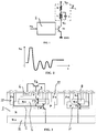
- an electric load ZL schematically represented by its equivalent electric circuit R-L-C, is connected to a circuit node at a voltage Vs.
- the load ZL is driven by a power device, specifically a bipolar transistor T1 of the NPN type, which is turned on and off by a signal from a driver circuit 1, known per se, under control by an appropriate input signal Vin.
- the output voltage of the power device is designated Vc.
- Shown in Figure 2 is the pattern vs. time of the voltage Vc when the transistor Tl is in the off state.
- This portion comprises an N+ doped substrate, indicated as region 2, wherein a power transistor T1 is formed whose collector, base and emitter regions are respectively defined by regions 3, 7 and 8. Formed in the region 2 as a part of the driver circuit 1, is a second transistor T4 whose collector, base and emitter regions are respectively defined by regions 4, 9 and 6.
- the transistor T4 is contained in an isolation well formed of a buried region 5 of the P type and two regions 10, 11 of the P+ type.
- the integrated structure just described implies the presence of two parasitic transistors T5 and T6.
- the base of the transistor T5 is in common with the collector of the transistor T6, formed in the region 4 of the N+ type, its emitter is formed in the region 9 of the P type, and its collector is in common with the base of the transistor T6, in the region 5 of the P type.
- the emitter of the transistor T6 is formed within the region 3 of the N type.
- connection pattern of the parasitic transistors T5, T6 is illustrated in Figure 3 by a wiring diagram superimposed on the cross-sectional representation of the integrated structure.
- the power device T1 consists of a bipolar transistor of the NPN type.
- the emitter of the transistor T1 is connected to ground, whilst its emitter is connected to a load ZL, specifically a coil or a transformer.
- the other end of the load ZL is connected to a node at a voltage Vs.
- the limiter circuit 40 Associated with the collector of the transistor T1 is a limiter circuit 40 for its related output voltage Vc.
- the limiter circuit 40 includes a semiconductor junction element, in particular a silicon controlled rectifier, or SCR, having an anode terminal A, a cathode terminal K, and a control terminal G.
- the anode terminal A is connected to the node at the voltage Vs
- the cathode terminal K is connected to the common circuit node between the power transistor T1 and the resonant load ZL
- the control terminal G is connected to the positive pole of a generator E of a predetermined value.
- the negative pole of this generator is connected to the circuit ground.
- the silicon controlled rectifier is formed of two transistors T2, T3 of a mutually complementary type.
- these transistors T2, T3 are bipolar transistors of the PNP and NPN type, respectively.
- the emitter of the first transistor T2 is the anode terminal A of the SCR, whereas the emitter of the second transistor T3 is the cathode terminal K of the diode.
- the collector of the first transistor T2 is connected to the base of the second transistor T3, and is the control terminal G of the SCR, and the base of the first transistor T2 is connected to the collector of the second transistor T3.
- FIG. 5 Also shown in Figure 5 is an embodiment circuit-wise of the fixed voltage generator E.
- This reference voltage is obtained through a diode D1 which is forward biased by a resistor R1.
- a terminal of this resistor is connected between the circuit node at the voltage Vs and the anode terminal of the diode D1, the cathode terminal of the diode D1 being connected to the circuit ground.
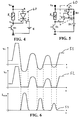
- the curve designated 51 represents the pattern vs. time of the voltage Vc present at the output node of the power device as the transistor T1 is turned off and in the absence of a limiter circuit for said output voltage. It can be seen that a positive overvoltage first establishes itself at said node which is followed by a series of negative voltage peaks.
- the curve designated 52 represents the pattern vs. time of the voltage Vc present at the output node of the power device as the transistor T1 is turned off, in the presence of the limiter circuit of this invention. It can be seen that the value of the voltage Vc remains positive all the time.
- the curve designated 53 illustrates the pattern vs. time of the current Is through the SCR 40.
- the controlled rectifier 40 will be conducting when the voltage between the control terminal G and the cathode terminal exceeds a given threshold value, typically in the 0.6 to 0.7 volts range.
- FIG. 7 Shown in Figure 7 is a vertical section view of the integrated structure of the limiter circuit depicted schematically in Figure 5, and of that of the power transistor T1.
- This structure comprises an N+ doped substrate, denoted by 2, wherein the power transistor T1, the two transistors T2 and T3, the resistor R1 and the diode D1 are formed.
- the collector, base and emitter regions of the power transistor T1 are respectively defined by the regions 3, 7 and 8.
- the two transistors T2, T3 of the limiter circuit in Figure 5 are formed in four superimposed layers which are doped with impurities of the P type and the N type, alternately. More specifically, the base of the transistor T2 is in common with the collector of the transistor T3 in a region 13 of the N+ type; its emitter is formed in a region 14 of the P type; its collector is in common with the base of the transistor T3 in a region 12 of the P type; and the emitter of the transistor T3 is formed within the region 3 of the N type.
- the structure of the regions forming such transistors substantially corresponds to the structure of the parasitic transistors T5, T6 present in the driver circuit portion shown in Figure 3.
- resistor R1 defined in a region 15 of the P type
- diode D1 having its anode formed in a region 16 of the P type and cathode formed in a region 17 of the N+ type.
- the silicon controlled rectifier contained in the limiter circuit 40, will be conducting current as the voltage between the control terminal G and the cathode terminal K exceeds a given threshold value, typically in the 0.6 to 0.7 volts range. Since the voltage at the control terminal G of the SCR is held constant by the voltage generator E, the diode will be conducting as the voltage at its cathode terminal K reaches a value close to zero volts. The current supplied to the load by the SCR maintains the voltage Vc at the collector of the power transistor T1 positive, as shown by the curve 52 in Figure 6.
- the limiter circuit 40 comprises two transistors T2, T3, respectively of the PNP and NPN type, and the voltage reference E is formed by a diode D1 forward biased by a resistor R1.
- the base of the transistor T3, which represents the control terminal of the SCR, is connected to the anode of the diode D1, whereby, when the voltage Vc tends to go negative, the transistor T3 begins conducting through the resistor R1; as a result, the transistor T2 will also be conducting and supply the resonant load with the required current to hold the collector of the transistor T1 at a voltage close to zero during the time when it would tend to go negative due to the capacitance present at the resonant load.
- the emitter-base junction of the transistor T3 is also to withstand that voltage.
- its base is connected to a potential of about 0.7 volts, whilst its emitter is connected to the collector of the high-voltage transistor T1.
- This junction which is to withstand high voltages, can be readily implemented in the VIPower technology employed for making the integrated structures shown in Figures 3 and 7.
- Figure 7 shows indeed an embodiment wherein the base-emitter junction of the transistor T3, the regions 3 and 12, is provided by diffused regions similar to those, the regions 3 and 7, utilized to form the collector and base, respectively, of the transistor T1, which is a high-voltage power transistor.
- this invention does provide a circuit for limiting the output voltage from a power transistor arranged to drive a resonant load, which circuit is quite simple construction-wise and affords significant savings in integrated circuit area compared to prior art solutions.
- the area occupied by the limiter circuit of this invention is ten times smaller than the area itzd by the prior circuit described in the above-referenced patent application EP-A-0 425 024.
- the manufacture of the circuit is specially advantageous where the circuit is implemented in the VIPower technology, as is normally used for power devices which incorporate a logic control portion.
Description
Claims (6)
- A circuit for limiting the output voltage (Vc) from a power transistor (T1) connected in series with a resonant load (ZL) between a first pole (Vs) of a supply voltage generator and a second pole of said generator (GND), comprising a semiconductor junction element (40) having a first terminal (A), connected to said first pole (Vs), a second terminal (K) connected to a common circuit node (Vc) between the power transistor (T1) and the resonant load (ZL) and a third terminal (G), said semiconductor junction element (40) being provided by first (T2) and second (T3) bipolar transistors of a mutually complementary type each having an emitter, a collector and a base, wherein the emitter of the first transistor forms the first terminal (A) of the semiconductor junction element (40), the base of the first transistor connects to the collector of the second transistor, the collector of the first transistor connects to the base of the second transistor to form the third terminal (G) of the semiconductor junction element (40) and the emitter of the second transistor forms the second terminal (K) of the semiconductor junction element (40), characterised in that the third terminal (G) of the semiconductor junction element (40) is connected to a voltage reference (E) of a predetermined value.
- A circuit according to Claim 1 characterised in that the semiconductor junction element (40) is a silicon controlled rectifier, or SCR, and said first (A), second (K) and third (G) terminals correspond, respectively, to the anode, cathode and control terminals.
- A circuit according to Claim 2, characterised in that said voltage reference (E) is obtained through a diode (D1), having an anode and a cathode terminal, forward biased by a resistor (R1).
- A circuit according to Claim 3, characterised in that said resistor (R1) is connected between the first pole (Vs) of the supply voltage generator and the anode terminal of the diode (D1), and the cathode terminal of the diode (D1) is connected to the second pole (GND) of the supply voltage generator.
- A circuit according to any of Claims 1 to 4, characterised in that the semiconductor junction element (40) is formed on a semiconductor substrate, along with said power transistor (T1), in four superimposed layers (3,12,13,14) alternately doped with impurities of the N type and the P type.
- A circuit according to Claim 5, characterised in that the cathode terminal (K) of the semiconductor junction element (40) is formed in the first (3) of said layers, doped with impurities of the N type; the control terminal (G) of the semiconductor junction element (40), corresponding to the base region of the second transistor (T3) and to the collector region of the first transistor (T2), is formed in the second (12) of said layers, doped with impurities of the P type; the anode terminal (A) of the semiconductor junction element (40), corresponding to the emitter region of the first transistor (T2), is formed in the fourth (14) of said layers, doped with impurities of the P type; and the collector region of the second transistor (T3) and the base region of the first transistor (T2) are formed in the third (13) of said layers, doped with impurities of the N type.
Priority Applications (5)
| Application Number | Priority Date | Filing Date | Title |
|---|---|---|---|
| EP94830556A EP0715409B1 (en) | 1994-11-30 | 1994-11-30 | Circuit for limiting the output voltage of a power transistor |
| DE69416595T DE69416595T2 (en) | 1994-11-30 | 1994-11-30 | Circuit for limiting the output voltage of a power transistor |
| US08/520,616 US5606278A (en) | 1994-11-30 | 1995-08-30 | Circuit for limiting the output voltage of a power transistor |
| JP7307683A JPH08237095A (en) | 1994-11-30 | 1995-11-27 | Circuit to restrict output voltage of power transistor |
| US09/258,090 USRE36998E (en) | 1994-11-30 | 1999-02-25 | Circuit for limiting the output voltage of a power transistor |
Applications Claiming Priority (1)
| Application Number | Priority Date | Filing Date | Title |
|---|---|---|---|
| EP94830556A EP0715409B1 (en) | 1994-11-30 | 1994-11-30 | Circuit for limiting the output voltage of a power transistor |
Publications (2)
| Publication Number | Publication Date |
|---|---|
| EP0715409A1 EP0715409A1 (en) | 1996-06-05 |
| EP0715409B1 true EP0715409B1 (en) | 1999-02-17 |
Family
ID=8218587
Family Applications (1)
| Application Number | Title | Priority Date | Filing Date |
|---|---|---|---|
| EP94830556A Expired - Lifetime EP0715409B1 (en) | 1994-11-30 | 1994-11-30 | Circuit for limiting the output voltage of a power transistor |
Country Status (4)
| Country | Link |
|---|---|
| US (2) | US5606278A (en) |
| EP (1) | EP0715409B1 (en) |
| JP (1) | JPH08237095A (en) |
| DE (1) | DE69416595T2 (en) |
Families Citing this family (4)
| Publication number | Priority date | Publication date | Assignee | Title |
|---|---|---|---|---|
| US5703520A (en) * | 1996-04-01 | 1997-12-30 | Delco Electronics Corporation | Integrated inductive load snubbing device using a multi-collector transistor |
| US6034561A (en) * | 1997-06-09 | 2000-03-07 | Delco Electronics Corporation | Integrated inductive load snubbing device |
| EP0997001B1 (en) * | 1997-07-08 | 2002-11-06 | Robert Bosch Gmbh | Circuit arrangement, in particular for triggering an ignition end stage |
| US7082934B2 (en) * | 2004-08-24 | 2006-08-01 | Ford Global Technologies, Llc | Controlling spark for an engine with controllable valves |
Family Cites Families (10)
| Publication number | Priority date | Publication date | Assignee | Title |
|---|---|---|---|---|
| US3662184A (en) * | 1968-01-19 | 1972-05-09 | Owens Illinois Inc | Electronic circuitry for a flat gaseous discharge display panel |
| DE2732512C2 (en) * | 1977-07-19 | 1979-09-13 | Frankl & Kirchner Gmbh & Co Kg Fabrik Fuer Elektromotoren U. Elektrische Apparate, 6830 Schwetzingen | Protective circuit arrangement for an electronic switching amplifier in front of an electromagnet |
| JPS5768680A (en) * | 1980-10-14 | 1982-04-27 | Fanuc Ltd | Control circuit for direct current brake |
| US4642491A (en) * | 1983-06-24 | 1987-02-10 | International Business Machines Corporation | Single transistor driver circuit |
| DE3546513A1 (en) * | 1985-04-25 | 1987-02-19 | Kloeckner Wolfgang Dr | Method and circuit for operating a gas inlet or exhaust valve |
| US5021694A (en) * | 1987-03-30 | 1991-06-04 | Nec Corporation | Circuit for driving a gated p-n-p-n device |
| IT1236627B (en) * | 1989-10-24 | 1993-03-25 | St Microelectronics Srl | CIRCUIT FOR LIMITING THE OUTPUT VOLTAGE OF A MONOLITHIC POWER DEVICE WITH A SEMICONDUCTOR THAT DRIVES A RESONANT LOAD CONNECTED TO A POWER SUPPLY |
| US5001373A (en) * | 1990-01-09 | 1991-03-19 | Ford Motor Company | Active clamp circuit with immunity to zener diode microplasmic noise |
| US5075568A (en) * | 1991-01-22 | 1991-12-24 | Allegro Microsystems, Inc. | Switching bipolar driver circuit for inductive load |
| US5347169A (en) * | 1992-09-08 | 1994-09-13 | Preslar Donald R | Inductive load dump circuit |
-
1994
- 1994-11-30 DE DE69416595T patent/DE69416595T2/en not_active Expired - Fee Related
- 1994-11-30 EP EP94830556A patent/EP0715409B1/en not_active Expired - Lifetime
-
1995
- 1995-08-30 US US08/520,616 patent/US5606278A/en not_active Ceased
- 1995-11-27 JP JP7307683A patent/JPH08237095A/en active Pending
-
1999
- 1999-02-25 US US09/258,090 patent/USRE36998E/en not_active Expired - Lifetime
Also Published As
| Publication number | Publication date |
|---|---|
| JPH08237095A (en) | 1996-09-13 |
| US5606278A (en) | 1997-02-25 |
| EP0715409A1 (en) | 1996-06-05 |
| USRE36998E (en) | 2000-12-26 |
| DE69416595T2 (en) | 1999-06-17 |
| DE69416595D1 (en) | 1999-03-25 |
Similar Documents
| Publication | Publication Date | Title |
|---|---|---|
| US5210479A (en) | Drive circuit for an insulated gate transistor having overcurrent detecting and adjusting circuits | |
| US4937639A (en) | Input protector device for semiconductor device | |
| JP3058699B2 (en) | Negative voltage clamp circuit for current control in inductive loads | |
| EP0431290A2 (en) | MOS switching circuit having gate enhanced lateral bipolar transistor | |
| US6248616B1 (en) | Method for suppressing parasitic effects in a junction-isolation integrated circuit | |
| EP0715409B1 (en) | Circuit for limiting the output voltage of a power transistor | |
| JPH0668709B2 (en) | Voltage stabilizer | |
| US5357157A (en) | Power MOSFET circuit including short circuiting means for detecting the potential of the source terminal | |
| US5119263A (en) | Negative overvoltage protection circuit for insulated vertical pnp transistors | |
| EP0250086A2 (en) | Electrical circuit utilizing a concentric collector PNP transistor | |
| US4962346A (en) | Transitory current recirculation through a power switching transistor driving an inductive load | |
| US6054740A (en) | Protection against overvoltages of an integrated MOS power transistor | |
| EP0041363B1 (en) | Schmitt trigger circuit with a hysteresis characteristic | |
| US4130767A (en) | Semiconductor switch | |
| IE71164B1 (en) | Protection of power integrated circuits against load voltage surges | |
| US5300805A (en) | Epitaxial tub bias structure for integrated circuits | |
| US4096400A (en) | Inductive load driving amplifier | |
| US4860065A (en) | Semiconductor integrated circuit device | |
| US5616971A (en) | Power switching circuit | |
| EP0607474B1 (en) | Semiconductor integrated circuit with layer for isolating elements in substrate | |
| US6815779B1 (en) | Integrated circuit including protection against polarity inversion of the substrate potential | |
| KR0129129B1 (en) | Semiconductor integrated circuit device | |
| US5539301A (en) | Monolithically integrated power output stage | |
| CA1111517A (en) | Inductive load driving amplifier | |
| US4689500A (en) | Comparator with substrate injection protection |
Legal Events
| Date | Code | Title | Description |
|---|---|---|---|
| PUAI | Public reference made under article 153(3) epc to a published international application that has entered the european phase |
Free format text: ORIGINAL CODE: 0009012 |
|
| AK | Designated contracting states |
Kind code of ref document: A1 Designated state(s): DE FR GB IT |
|
| 17P | Request for examination filed |
Effective date: 19961123 |
|
| 17Q | First examination report despatched |
Effective date: 19970711 |
|
| GRAG | Despatch of communication of intention to grant |
Free format text: ORIGINAL CODE: EPIDOS AGRA |
|
| GRAG | Despatch of communication of intention to grant |
Free format text: ORIGINAL CODE: EPIDOS AGRA |
|
| GRAH | Despatch of communication of intention to grant a patent |
Free format text: ORIGINAL CODE: EPIDOS IGRA |
|
| RAP3 | Party data changed (applicant data changed or rights of an application transferred) |
Owner name: STMICROELECTRONICS S.R.L. |
|
| GRAH | Despatch of communication of intention to grant a patent |
Free format text: ORIGINAL CODE: EPIDOS IGRA |
|
| GRAA | (expected) grant |
Free format text: ORIGINAL CODE: 0009210 |
|
| AK | Designated contracting states |
Kind code of ref document: B1 Designated state(s): DE FR GB IT |
|
| REF | Corresponds to: |
Ref document number: 69416595 Country of ref document: DE Date of ref document: 19990325 |
|
| ET | Fr: translation filed | ||
| PLBE | No opposition filed within time limit |
Free format text: ORIGINAL CODE: 0009261 |
|
| STAA | Information on the status of an ep patent application or granted ep patent |
Free format text: STATUS: NO OPPOSITION FILED WITHIN TIME LIMIT |
|
| 26N | No opposition filed | ||
| REG | Reference to a national code |
Ref country code: GB Ref legal event code: IF02 |
|
| PGFP | Annual fee paid to national office [announced via postgrant information from national office to epo] |
Ref country code: DE Payment date: 20031211 Year of fee payment: 10 |
|
| PG25 | Lapsed in a contracting state [announced via postgrant information from national office to epo] |
Ref country code: DE Free format text: LAPSE BECAUSE OF NON-PAYMENT OF DUE FEES Effective date: 20050601 |
|
| PGFP | Annual fee paid to national office [announced via postgrant information from national office to epo] |
Ref country code: FR Payment date: 20051108 Year of fee payment: 12 |
|
| PG25 | Lapsed in a contracting state [announced via postgrant information from national office to epo] |
Ref country code: IT Free format text: LAPSE BECAUSE OF NON-PAYMENT OF DUE FEES;WARNING: LAPSES OF ITALIAN PATENTS WITH EFFECTIVE DATE BEFORE 2007 MAY HAVE OCCURRED AT ANY TIME BEFORE 2007. THE CORRECT EFFECTIVE DATE MAY BE DIFFERENT FROM THE ONE RECORDED. Effective date: 20051130 |
|
| PGFP | Annual fee paid to national office [announced via postgrant information from national office to epo] |
Ref country code: GB Payment date: 20051130 Year of fee payment: 12 |
|
| GBPC | Gb: european patent ceased through non-payment of renewal fee |
Effective date: 20061130 |
|
| REG | Reference to a national code |
Ref country code: FR Ref legal event code: ST Effective date: 20070731 |
|
| PG25 | Lapsed in a contracting state [announced via postgrant information from national office to epo] |
Ref country code: GB Free format text: LAPSE BECAUSE OF NON-PAYMENT OF DUE FEES Effective date: 20061130 |
|
| PG25 | Lapsed in a contracting state [announced via postgrant information from national office to epo] |
Ref country code: FR Free format text: LAPSE BECAUSE OF NON-PAYMENT OF DUE FEES Effective date: 20061130 |