EP0714780B1 - Method and apparatus for thermal printing with voltage-drop compensation - Google Patents
Method and apparatus for thermal printing with voltage-drop compensation Download PDFInfo
- Publication number
- EP0714780B1 EP0714780B1 EP95203025A EP95203025A EP0714780B1 EP 0714780 B1 EP0714780 B1 EP 0714780B1 EP 95203025 A EP95203025 A EP 95203025A EP 95203025 A EP95203025 A EP 95203025A EP 0714780 B1 EP0714780 B1 EP 0714780B1
- Authority
- EP
- European Patent Office
- Prior art keywords
- heating elements
- data
- strobe signal
- power
- voltage
- Prior art date
- Legal status (The legal status is an assumption and is not a legal conclusion. Google has not performed a legal analysis and makes no representation as to the accuracy of the status listed.)
- Expired - Lifetime
Links
- 238000000034 method Methods 0.000 title claims description 27
- 238000007651 thermal printing Methods 0.000 title claims description 8
- 238000010438 heat treatment Methods 0.000 claims description 118
- 230000003213 activating effect Effects 0.000 claims description 16
- 238000000859 sublimation Methods 0.000 claims description 14
- 230000008022 sublimation Effects 0.000 claims description 14
- 238000012360 testing method Methods 0.000 claims description 12
- 230000004913 activation Effects 0.000 claims description 10
- 239000007787 solid Substances 0.000 claims description 10
- 238000012937 correction Methods 0.000 claims description 8
- 238000012545 processing Methods 0.000 claims description 8
- 239000000975 dye Substances 0.000 description 16
- 238000007639 printing Methods 0.000 description 14
- 238000010586 diagram Methods 0.000 description 10
- 238000006243 chemical reaction Methods 0.000 description 6
- 239000011159 matrix material Substances 0.000 description 6
- 238000012546 transfer Methods 0.000 description 6
- 238000013507 mapping Methods 0.000 description 5
- 230000007423 decrease Effects 0.000 description 4
- 238000009792 diffusion process Methods 0.000 description 4
- 230000000694 effects Effects 0.000 description 4
- 230000006870 function Effects 0.000 description 3
- 230000004048 modification Effects 0.000 description 3
- 238000012986 modification Methods 0.000 description 3
- 230000003287 optical effect Effects 0.000 description 3
- 230000008901 benefit Effects 0.000 description 2
- 238000010276 construction Methods 0.000 description 2
- 238000001816 cooling Methods 0.000 description 2
- 230000003247 decreasing effect Effects 0.000 description 2
- 230000003190 augmentative effect Effects 0.000 description 1
- 230000005540 biological transmission Effects 0.000 description 1
- 239000000919 ceramic Substances 0.000 description 1
- 239000002131 composite material Substances 0.000 description 1
- 238000013461 design Methods 0.000 description 1
- 238000003745 diagnosis Methods 0.000 description 1
- 230000010354 integration Effects 0.000 description 1
- 230000007246 mechanism Effects 0.000 description 1
- 230000008569 process Effects 0.000 description 1
- 238000003908 quality control method Methods 0.000 description 1
- 230000009467 reduction Effects 0.000 description 1
- 230000000930 thermomechanical effect Effects 0.000 description 1
- 230000009466 transformation Effects 0.000 description 1
Images



Classifications
-
- B—PERFORMING OPERATIONS; TRANSPORTING
- B41—PRINTING; LINING MACHINES; TYPEWRITERS; STAMPS
- B41J—TYPEWRITERS; SELECTIVE PRINTING MECHANISMS, i.e. MECHANISMS PRINTING OTHERWISE THAN FROM A FORME; CORRECTION OF TYPOGRAPHICAL ERRORS
- B41J2/00—Typewriters or selective printing mechanisms characterised by the printing or marking process for which they are designed
- B41J2/315—Typewriters or selective printing mechanisms characterised by the printing or marking process for which they are designed characterised by selective application of heat to a heat sensitive printing or impression-transfer material
- B41J2/32—Typewriters or selective printing mechanisms characterised by the printing or marking process for which they are designed characterised by selective application of heat to a heat sensitive printing or impression-transfer material using thermal heads
- B41J2/35—Typewriters or selective printing mechanisms characterised by the printing or marking process for which they are designed characterised by selective application of heat to a heat sensitive printing or impression-transfer material using thermal heads providing current or voltage to the thermal head
- B41J2/355—Control circuits for heating-element selection
- B41J2/36—Print density control
Definitions
- the present invention relates to thermal dye diffusion printing, further commonly referred to as sublimation printing, and more particularly to a method for correcting uneveness in the printed density of a thermal sublimation print.
- Thermal sublimation printing uses a dye transfer process, in which a carrier containing a dye is disposed between a receiver, such as a transparent film or a paper, and a print head formed of a plurality of individual heat producing elements which will be referred to as heating elements.
- the receiver is mounted on a rotatable drum.
- the carrier and the receiver are generally moved relative to the print head which is fixed.
- a particular heating element is energised, it is heated and causes dye to transfer, e.g. by diffusion or sublimation, from the carrier to an image pixel (or "picture element") in the receiver.
- the density of the printed dye is a function of the temperature of the heating element and the time the carrier is heated.
- the heat delivered from the heating element to the carrier causes dye to transfer to the receiver to make thereon an image related to the amount of heat.
- Thermal dye transfer printer apparatus offer the advantage of true "continuous tone" dye density transfer. By varying the heat applied by each heating element to the carrier, an image pixel with a variable density is formed in the receiver.
- Voltage drop effects may be caused by the fact that the voltage V applied to the heating elements is not constant, and hence, as a result, the driven heating elements H i do not generate a constant quantity of heat.
- US 5,109,235 discloses a recorder wherein the number of pulses applied to the plurality of heating resistors in the thermal head is counted every gradation level and the applied pulse width (or the amplitude) is changed.
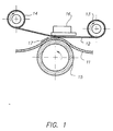
- FIG 1 there is shown a global principal scheme of a thermal printing apparatus that can be used in accordance with the present invention and which is capable to print a line of pixels at a time on a receiver or acceptor member 11 from dyes transferred from a carrier or dye donor member 12.
- the receiver 11 is in the form of a sheet; the carrier 12 is in the form of a web and is driven from a supply roller 13 onto a take up roller 14.
- the receiver 11 is secured to a rotatable drum or platen 15, driven by a drive mechanism (not shown for purpose of simplicity) which advances the drum 15 and the receiver sheet 11 past a stationary thermal head 16. This head 16 presses the carrier 12 against the receiver 11 and receives the output of the driver circuits.
- the thermal head 16 normally includes a plurality of heating elements equal in number to the number of pixels in the image data present in a line memory.
- the imagewise heating of the dye donor element is performed on a line by line basis, with the heating resistors geometrically juxtaposed each along another and with gradual construction of the printed density.
- Each of these resistors is capable of being energised by heating pulses, the energy of which is controlled in accordance with the required density of the corresponding picture element.
- the output energy increases and so the optical density of the hardcopy image 17 on the receiving sheet.
- lower density image data cause the heating energy to be decreased, giving a lighter picture 17.
- the activation of the heating elements is preferably executed pulsewise and preferably by digital electronics.
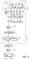
- the different processing steps up to the activation of said heating elements are illustrated in the diagram of Fig 2.
- First a digital signal representation is obtained in an image acquisition apparatus 18.
- the image signal is applied via a digital interface 19 and a first storing means (indicated as MEMORY in Fig. 2) to a recording unit 21, namely a thermal sublimation printer.
- the digital image signal is processed 23, which is explained more thoroughly in other patent applications.
- the recording head (16) is controlled so as to produce in each pixel the density value corresponding with the processed digital image signal value.
- a stream of serial data of bits is shifted into another storing means, e.g. a shift register 26, representing the next line of data that is to be printed.
- these bits are supplied in parallel to the associated inputs of a latch register 27.
- the bits of data from the shift register 26 are stored in the latch register 27, another line of bits can be sequentially clocked into said shift register 26.
- the heating elements 28 the upper terminals are connected to a positive voltage source (indicated as V TH in Fig.
- the present invention offers an advantageous solution to this problem.
- the method of thermal recording comprises the steps of:
- the first step (a) of a method according to the present invention comprises the supplying of parallel formatted input data I u to a processing unit 23 of a thermal printer having a line type thermal head with a plurality of heating elements H i ( 28).
- the electrical image data are available at the input of processing unit 23.
- Said data are generally provided as binary pixel values, which are in proportion to the densities of the corresponding pixels in the image.
- an image signal matrix is a twodimensional array of quantised density values or image data I(i,j) where i represents the pixel column location and j represents the pixel row location, or otherwise with i denoting the position across the head of the particular heating element and j denoting the line of the image to be printed.
- an image with a 2880 x 2086 matrix will have 2880 columns and 2086 rows, thus 2880 pixels horizontally and 2086 pixels vertically.
- the content of said matrix is a number representing the density to be printed in each pixel, whereby the number of density values of each pixel to be reproduced is restricted by the number of bits pro pixel.
- the image signal matrix to be printed is preferably directed to an electronic lookup table 22 (abbreviated as LUT) which correlates the density to the number of pulses to be used to drive each heating element (H i ) in the thermal print head. This number will further be referred to as processed input data (I p ).
- LUT electronic lookup table 22
- these pulses may be corrected by correlating each of the strings of pulses to density correcting methods.
- these pulses may be processed such that an optimal diagnostic perceptibility is obtained, as described in published European patent application EP 0 536 822 A1 (in the name of Agfa-Gevaert). Thereafter, the processed pulses are directed to the head driver for energizing the thermal heating elements within the thermal head.
- the second step (b) comprises a storing of processed input data I p representing image information of one line of the image, into a line buffer memory 24, whereafter said data are called "input line data I l " .
- the electronical image data are mostly available (e.g. from a host computer) in a "parrallel format" (e.g. bytes consisting of eigth bits), whereas the gradual construction (cfr. Figs. 3 and 4, both to be explained further on) of a printed density on a receiver by thermal recording needs a (time-) "serial" format of the output drive signals.
- a parrallel format e.g. bytes consisting of eigth bits
- a parallel-to-serial conversion of the input line data I l of which a preferred embodiment is described in published patent application EP 0 520 093 A1 (in the name of Agfa-Gevaert), is also included in the present application,
- the serial formatted line data will be indicated by the symbol I s .
- the thermal head normally includes a plurality of heating elements equal in number to the number of pixels in the data present in the line memory and that each of the heating elements is capable of being energized by heating pulses, the number of which is controlled in accordance with the required density of the corresponding picture element
- Fig. 3 illustrates the conversion of a ten-head-row subjected to image data of bytes consisting of two bits, and thus representing maximally four densities. It follows that the thermal head applied with a recording pulse causes current to flow through corresponding "ones" (cfr. input data indicative of "black picture elements" ) of the electrodes.
- Integration of all (time-serial) heating pulses corresponding with consecutive gradation or density levels d i determines the total recording energy and thus the resulting printed density D i .
- the output energy increases proportionally, thereby augmenting the optical density Di on the receiving sheet.
- lower density image data cause the output energy to be decreased, giving a lighter picture.
- Figure 4 is a graph illustrating serial formatted image data I s representing 2 K gradation levels d i as these data are available at the exit of the parallel to serial conversion means 25.
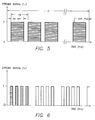
- Duty cycled pulsing is indicated in Fig. 5, showing the current pulses applied to a single heating element (refs. H i and 28 in Fig. 2).
- the repetition strobe period (t s ) consists of one heating cycle (t son ) and one cooling cycle (t s - t son ) as indicated in the same Fig. 5.
- the strobe pulse width (t son ) is the time an enable strobe signal is on.
- the strobe duty cycle of a heating element is the ratio of the pulse width (t son ) to the repetition strobe period (t s ).
- the strobe period (t s ) preferably is a constant, but the pulse width (t son ) may be adjustable, according to a precise rule which will be explained later on; so the strobe duty cycle may be varied accordingly.
- the line time (t l ) is divided in a number (N) of strobe pulses each with repetition strobe periods t s as indicated on Fig. 5.
- N the number of strobe pulses each with repetition strobe periods t s as indicated on Fig. 5.
- the maximal diffusion time would be reached after 1024 sequential strobe periods.
- an equal time averaged power P ave is made available to the heating elements, although their individual characteristics, as resistance value and time delay in the switching circuit may be different.
- an equal time averaged power P ave is understood that the power available to the heating elements of the thermal head is kept constant during each strobe period (t s ), meaning that the average value of the power during a heating time or strobe-on time (t s,on ) and during a cooling time or strobe-off time (t s - t s,on ) is equal for all heating elements, irrespective of differences in resistance values etc.
- t s strobe period
- an array of power corrections 31 may be obtained, also referred to as "power map", to obtain power corrected image signals.
- This array gives for each heating element (H i ) the "power compensation data" R p intended for equidistant skipping of the strobe pulses. This thus guarantees an equal time averaged power available to the heating elements (H i ), although their individual characteristics, as resistance value (cfr. Ref. 28) and time delay in the switching circuit (cfr. Ref. 29), may be different.
- such power map 31 may be implemented in the form of a lookup table.
- a power compensation R p is memorised, comprising pro each gradation or density level a row of binary 0 's and 1 's such that the heating element with the highest resistance and which, per consequence, could only dissipate a rather low power, is allowed to dissipate fully naturally.
- the power map will present a R p value consisting of 1024 times 1 (thus 111...111).
- another heating element which normally would dissipate e.g.
- every fifth strobe pulse may be skipped as illustrated by Fig. 6; and hence, in the case of a 10 bit pixel depth, the power map will present a R p value 1111011110.... All other heating elements will have R p values in between them, as e.g. 10101010...
- Fig. 7 is an array of power compensation data R p intended for equidistant skipping of strobe pulses and also referred to as "power map".
- the fourth step (d) comprises a capturing (31) of resistance compensation data R p and a mapping (32) of the serial configurated data I s with said resistance compensation data R p into so-called "power mapped" data I m .
- step (d) A preferred embodiment for carrying out step (d) is shown in figure 8, which illustrates a mapping of serial configurated image-pixeldata with resistance compensation data into so-called power-mapped data according to the present invention.
- Fig. 9 is a chart illustrating for all heating elements the activating heating pulses with an exemplary duty-cycle and with an exemplary skipping.
- skipped pulses are indicated by dotted lines.
- the power mapped data I m have been corrected for equal time averaged power, although individual characteristics of the heating elements may be different, as resistance value and time delay in the switching circuit.
- thermomechanical nonuniformities e.g. variations in the mechanical or thermal contact between the thermal head and the back of the dye donor sheet, or variations in the thermal contact between the ceramic base of the head assembly and the heatsink, etc.
- a solution to this problem has been disclosed in patent application EP 94.201.310.3. Another possible reason which may cause such undesired variations precisely relates to the voltage-drop phenomen as indicated herabove.
- a fifth step (e) in the method of the present application comprises a shifting of said power mapped data I m (further called shifted power mapped data I m' ) into a shift buffer memory 26 and meanwhile counting ( cfr. Ref. 33) a number N s,on of simultaneously activated heating elements.
- a sixth step (f) in the method of the present application comprises an adapting (cfr. Ref. 34) of a strobe duty cycle ⁇ (from generator 35) in accordance with said number N s,on , further called “voltage corrected strobe duty cycle ⁇ v ".
- a next step (g) the voltage corrected strobe duty cycle ⁇ v and the shifted power mapped data I m' are provided via an AND-gate 36 to driving means 29 of the thermal head, thereby activating the heating elements 28 for reproducing the image.
- the printed density is a function of the applied energy (for a fixed time averaged power).
- the activation of the heating elements is preferably executed pulsewise, and thus the printed density has to be related to a time averaged power.
- figure 10 is a simplified circuit diagram of a thermal head showing components, currents and voltages, including heating elements Hi with resistance values R e,i .
- the common wiring from the power supply 42 to the individual heating elements 28 inside the thermal head can be represented by a common resistance R C (Ref. 44).
- R C Resf. 44
- V TH indicates the voltage of the power supply
- V d indicates the voltage drop over the common wiring
- V e indicates the voltage drop over the heating elements
- V l indicates the voltage drop over the switching means (which itself is illustrated in Figs. 2 and 12 by a transistor with referral 29)
- I c indicates the current through the common wiring
- I e indicates the current through the heating elements.
- an electrical current through the heating elements of the thermal head causes a voltage drop over the wiring from the power supply to the heating elements inside the head. Because of the specific way of pulsewise activating according to the present invention (cfr. Fig. 5), this voltage drop happens during the strobe-on time t s,on and increases with the number N s,on of heating elements active at that moment. As a consequence, the dissipated power in the active heating elements, and therefore also the generated heat and the obtained density, depend on the number of activated heating elements. Evidently, the highest voltage drop is caused by the wiring common to all the elements, because the sum of all the electrical currents can flow through it.
- a solution to the voltage drop problem comprises a proportional increase of the active strobe time t s,on as the voltage V e over the heating elements decreases. More specifically: in every strobe period the average power during that strobe period is increased by stretching the t son of that strobe period and thus increasing the strobe duty cycle.
- an intermediate step may be introduced, comprising a processing of the parallel formatted input data I u , said data further being indicated by I p .
- an intermediate step comprising bringing the shifted power mapped data I m' from a shift buffer memory (26) into a latching buffer memory (27), said data further being indicated by I m'' .
- the thermal recording is preferably carried out at least at two gradation (or density) levels.
- the counting of a number N s,on of simultaneously activated heating elements is carried out at each gradation level.
- the adapting of a strobe duty cycle ⁇ is carried out at least at one gradation level.
- the adapting of a strobe duty cycle is carried out at a spaced number of gradation levels; e.g. each 8th gradation level.
- the providing of the voltage corrected strobe duty cycle ⁇ v and the power mapped data I p is carried out at least at one gradation level.
- the providing of the voltage corrected strobe duty cycle and the power mapped data is carried out at a spaced number of gradation levels.
- said providing of the voltage corrected strobe duty cycle and the power mapped data is carried out at each gradation level.
- a thermal printer comprising a thermal head having a plurality of heating elements, means for selectively activating each heating element, wherein said activating is executed pulse-wise with an adjustable strobe duty-cycle ⁇ , means for equalizing while printing the time averaged power P ave dissipated by each heating element; counting means (33) for counting a number N s,on of heating elements simultaneously activated at each gradation level d i ; and controlling means (34) for controlling the strobe duty-cycle at each gradation level in accordance with said number N s,on of heating elements counted by the counting means.
- FIG. 11 illustrates a partial block diagram of an activation of the heating elements in connection with a voltage drop compensation according to the present invention
- figure 12 illustrates a data flow diagram of a preferred embodiment of a thermal sublimation printer according to the present invention.
- each heating element H i in a thermal head receives an electrical energization signal I ih that itself is a composite of two other electrical signals.
- the energization signal is a logical AND (cfr. referral 36) of a voltage drop compensated strobe signal (from generator 35) and a power mapped data signal I m'' .
- the strobe signal which is periodically sent to each of the heating elements consists of two portions, i.c. an initial on-time and a subsequent off-time (cfr. also Fig. 5).
- the data signal determines whether, within the period of the signal of the strobe signal, any portion of the strobe signal should be applied to a heating element to cause it to print.
- the diagram of Fig. 12 may in practice be often more complicated, in that it generally will be necessary to apply corrections to the image data before these data are used to obtain an image of high quality.
- Type and extent of corrections will also depend on the particular dye donor element being used. For example a different type of correction will generally be necessary when printing a black and white image using a black dye donor element than when a color image is being printed with a dye donor element having a series of differently colored dye frames.
- Other corrections may include differences in electrical characteristics of the heating elements and/or in physical characteristics of the contact between thermal head, donor element, receiver element and printing drum.
- An appropriate model is described in patent application EP-A- 671276 (in the name of Agfa-gevaert).
- a method is implemented wherein the step of converting the input data into processed image data also comprises corrections.
- Such control of a voltage drop phenomen preferably comprises a test pattern comprising solid "white” areas (which are not written at any density), alternated with solid “black” areas. These black areas preferably result from activating each heating element corresponding to that area with input image data, also called “power mapped input data I i,m ", so that a same time-averaged power is generated in each heating element to obtain a flat field area.
- a first zone A e.g. some 100 lines may be fully written over the total width of the receiver; then, in a zone B, some 100 lines with solid blacks over the first x % (say 25 %) width and over the last y % (say also 25 %) and solid white over the remaining (100-x-y)% (say 50 %).
- a zone C again e.g. some 100 lines may be fully written over the total width of the receiver; then, in a zone D, some 100 lines with solid blacks over the first x % (say 30 %) width and over the last y % (say also 30 %) and solid white over the remaining (100-x-y)% (say 40 %); etc.
- the results of the printed test pattern are evaluated by estimating the deviation of the printed density in a total black area (as zones A and C) versus the printed density in a partly black area (as zones B and D).
- a solution to the voltage drop problem comprises an empirical increase or decrease of the active strobe time t s,on until the printed densitiy in zones A, B, C and D are all equal.
- the amount of energy supplied to the heating elements is controlled in accordance with the number of active heating elements, there is no reduction in the recording quality, such as irregularities in the density within a line.
- the method of the present invention provides a remarkable eveness in the printed density, said method is very well suited to be used in medical diagnosis.
- the printing may be applied in graphic representations, in facsimile transmission of documents etc.
- This invention may be used for greyscale thermal sublimation printing as well as for color thermal sublimation printing.
- a set of color selection image input data I u representing yellow, magenta, cyan and black color components of the original color image, respectively are captured.
- the electrical signals corresponding to the different color selections are processed.
- the color component signals are supplied to respective gradation correction circuits, in which gradation curves suitable for correcting the respective gradations for the yellow, magenta, cyan and black components are stored; preferably said signals are subjected to typical corresponding transformation lookup tables (LUT's).
- the present invention can be implemented for a thermal printer apparatus of other systems such as a heat transfer recorder using e.g. an resistive ribbon printing, using thermal wax printing or using direct thermal printing.
Landscapes
- Electronic Switches (AREA)
Description
As already mentioned before, the electrical image data are available at the input of processing unit 23. Said data are generally provided as binary pixel values, which are in proportion to the densities of the corresponding pixels in the image. For a good understanding of said proportion, it is noted that an image signal matrix is a twodimensional array of quantised density values or image data I(i,j) where i represents the pixel column location and j represents the pixel row location, or otherwise with i denoting the position across the head of the particular heating element and j denoting the line of the image to be printed. For example, an image with a 2880 x 2086 matrix will have 2880 columns and 2086 rows, thus 2880 pixels horizontally and 2086 pixels vertically. The content of said matrix is a number representing the density to be printed in each pixel, whereby the number of density values of each pixel to be reproduced is restricted by the number of bits pro pixel. For a K bit deep image matrix, individual pixels can have N = 2K density values, ranging from 0 to 2K - 1. If the matrix depth or pixel depth is 8 bits, the image can have up to 28 or 256 density values.
Because of the specific way of pulsewise activating according to the present invention (cfr. Fig. 5), this voltage drop happens during the strobe-on time ts,on and increases with the number Ns,on of heating elements active at that moment.
As a consequence, the dissipated power in the active heating elements, and therefore also the generated heat and the obtained density, depend on the number of activated heating elements. Evidently, the highest voltage drop is caused by the wiring common to all the elements, because the sum of all the electrical currents can flow through it.
- the resistance value of the common wiring was tuned experimentally between 10 and 40 mΩ, often it amounted e.g. to Rc ≅ 24 mΩ;
- the maximal voltage drop occuring if all heating elements were activated was found experimentally to be between 0.1 and 0.6 V, and amounted e.g. to ΔVmax ≅ 0.35;
- the maximal decrease in average power was found experimentally to be between .5 and 4.0 mW, e.g. ΔPmax ≅ 2.7 mW;
- the maximal decrease in optical density was found experimentally to be between 0.1D and 0.5 D, and amounted e.g. to ΔD ≅ 20 points for yellow Y, 22 points for magenta M and 35 points for cyan C.
From Figs. 5 and 10, it may be derived that the time averaged power dissipated in a heating element is given by
Claims (7)
- A method for adjusting the thermal recording of a thermal printer (21), said thermal printer havingsaid plurality of heating elements being capable of being activated only while said strobe signal is at said first voltage,a line- type thermal printing head (16) with a plurality of heating elements (28),storage means (31) for storing resistance compensation data associated with said plurality of heating elements, anda strobe generation means (35) for repeatedly generating a strobe signal having N cycles in a line time tl, said strobe signal havinga first voltage during a first percentage of each cycle anda second voltage during a second percentage of each cycle,
the method comprising the steps of :a) supplying input data to said thermal printer, said input data representing a test pattern to be thermally recorded on a receiving medium (17), said test pattern comprising zones (A,B,C,D), at least one zone (A,C) has a solid black area which covers the full width of said receiving medium, at least one zone (B,D) has solid black areas which together cover less than the full width of said receiving medium;b) converting said input data into power- mapped data Im using said resistance compensation data Rp;c) for each of said N cycles of said strobe signal, counting the number of said plurality of heating elements to be activated from said power- mapped data;d) for each of said N cycles of said strobe signal, adjusting said first percentage of each cycle for which said first voltage is generated in accordance with said number of heating elements to be activated;e) for each of said N cycles of said strobe signal, activating said plurality of heating elements in accordance with said power- mapped data and said strobe signal;f) repeating steps (b) to (e) until said test pattern is printed on said receiving medium;g) estimating a deviation between the printed density of the different zones of said test pattern printed on said receiving medium; andh) adjusting said first percentage of each cycle for which said first voltage is generated in accordance with said deviation. - A method for adjusting the thermal recording of a thermal printer (21), said thermal printer havingthe method comprising the steps of :a line- type thermal printing head (16) with a plurality of heating elements (28),storage means (31) for storing resistance compensation data Rp associated with said plurality of heating elements,a strobe generation means (35) for repeatedly generating a strobe signal having N cycles in a line time tl, said strobe signal havinga first voltage during a first percentage of each cycle anda second voltage during a second percentage of each cycle, andgated driving means (29) forallowing the activation of said plurality of heating elements while said strobe signal is at said first voltage andprohibiting the activation of said plurality of heating elements while said strobe signal is at said second voltagea) supplying input data to said thermal printer, said input data representing a test pattern to be thermally recorded on a receiving medium (17), said test pattern comprising zones (A,B,C,D), at least one zone (A,C) has a solid black area which covers the full width of said receiving medium, at least one zone (B,D) has solid black areas which together cover less than the full width of said receiving medium;b) storing a portion of said input data in a line buffer memory (24), said portion of said input data representing one line of said test pattern to be printed on said receiving medium;c) converting said portion of said input data into serial configured data Is;d) converting said serial configured data Is into power- mapped data Im using said resistance compensation data Rp;e) for each of said N cycles of said strobe signal, consecutively shifting each power- mapped activation sequence of said power- mapped data Im into a shift buffer memory (26);f) for each power- mapped activation sequence, counting the number of said plurality of heating elements to be activated from each sequence;g) for each of said N cycles of said strobe signal, adjusting said first percentage of each cycle for which said first voltage is generated in accordance with said number of heating elements to be activated;h) for each of said N cycles of said strobe signal, providing said shifted power- mapped activation sequence to said gated driving for each of said N cycles of said strobe signal, activating said plurality of heating elements in accordance with said shifted power- mapped data and said strobe signal;i) repeating steps (b) to (j) until said test pattern is printed on said receiving medium;k) estimating a deviation between the printed density of the different zones of said test pattern printed on said receiving medium; andl) adjusting said first percentage of each cycle for which said first voltage is generated in accordance with said deviation.
- The method according to claim 1 or 2, wherein said input data comprises colour data, and further comprising the step of processing said input data by colour gradation correction circuits after the step of supplying input data to said thermal printer.
- The method according to claim 2, further comprising the step of latching said shifted power- mapped data Im into a latching buffer memory, after step (e).
- The method according to claim 1 or 2, wherein said input data and said power- mapped data Im have at least two gradation levels.
- The method according to claim 1 or 2, wherein
a terminal of each of said heating elements (28) is connected to a common node and said common node is electrically coupled to a power source,
and wherein
said step of adjusting said first percentage of each cycle for which said first voltage is generated in accordance with said number of heating elements to be activated (Nson) further comprises
adjusting said first percentage of each cycle in accordance withthe unadjusted value of said first percentage of each cycle (tson),the resistance between said common node and said power source (Rc),the total number of said heating elements (Ne), andan equivalent resistance value for the heating elements in said thermal printing head (Rpar). - The method according to claim 1 or 2, wherein said thermal recording is performed by thermal sublimation.
Applications Claiming Priority (2)
| Application Number | Priority Date | Filing Date | Title |
|---|---|---|---|
| EP94203465 | 1994-11-29 | ||
| EP94203465 | 1994-11-29 |
Publications (2)
| Publication Number | Publication Date |
|---|---|
| EP0714780A1 EP0714780A1 (en) | 1996-06-05 |
| EP0714780B1 true EP0714780B1 (en) | 1999-03-17 |
Family
ID=8217417
Family Applications (1)
| Application Number | Title | Priority Date | Filing Date |
|---|---|---|---|
| EP95203025A Expired - Lifetime EP0714780B1 (en) | 1994-11-29 | 1995-11-08 | Method and apparatus for thermal printing with voltage-drop compensation |
Country Status (4)
| Country | Link |
|---|---|
| US (1) | US5786837A (en) |
| EP (1) | EP0714780B1 (en) |
| JP (1) | JPH08276610A (en) |
| DE (1) | DE69508351T2 (en) |
Families Citing this family (16)
| Publication number | Priority date | Publication date | Assignee | Title |
|---|---|---|---|---|
| US6532032B2 (en) * | 1999-05-07 | 2003-03-11 | Fargo Electronics, Inc. | Printer using thermal printhead |
| US6999202B2 (en) | 2001-03-27 | 2006-02-14 | Polaroid Corporation | Method for generating a halftone of a source image |
| US6842186B2 (en) * | 2001-05-30 | 2005-01-11 | Polaroid Corporation | High speed photo-printing apparatus |
| US6937365B2 (en) | 2001-05-30 | 2005-08-30 | Polaroid Corporation | Rendering images utilizing adaptive error diffusion |
| ATE303901T1 (en) * | 2001-05-30 | 2005-09-15 | Polaroid Corp | HIGH SPEED PHOTO PRINTING MACHINE |
| US6906736B2 (en) | 2002-02-19 | 2005-06-14 | Polaroid Corporation | Technique for printing a color image |
| CA2476905C (en) * | 2002-02-22 | 2007-10-30 | Polaroid Corporation | Common mode voltage correction |
| EP1431045A1 (en) * | 2002-12-17 | 2004-06-23 | Agfa-Gevaert | A modeling method for taking into account thermal head and ambient temperature. |
| EP1431044A1 (en) | 2002-12-17 | 2004-06-23 | Agfa-Gevaert | A deconvolution scheme for reducing cross-talk during an in the line printing sequence |
| US7283666B2 (en) | 2003-02-27 | 2007-10-16 | Saquib Suhail S | Digital image exposure correction |
| US8773685B2 (en) | 2003-07-01 | 2014-07-08 | Intellectual Ventures I Llc | High-speed digital image printing system |
| US6976752B2 (en) * | 2003-10-28 | 2005-12-20 | Lexmark International, Inc. | Ink jet printer with resistance compensation circuit |
| US7319473B2 (en) * | 2005-12-22 | 2008-01-15 | Carestream Health, Inc. | Thermal recording system and method |
| US11513042B2 (en) | 2015-01-26 | 2022-11-29 | SPEX SamplePrep, LLC | Power-compensated fusion furnace |
| US10240870B2 (en) * | 2015-01-26 | 2019-03-26 | Spex Sample Prep, Llc | Method for operating a power-compensated fusion furnace |
| WO2026035599A1 (en) * | 2024-08-06 | 2026-02-12 | Entrust Corporation | Identification card printer thermal print head with custom thermal compensation routine determination |
Family Cites Families (10)
| Publication number | Priority date | Publication date | Assignee | Title |
|---|---|---|---|---|
| US4688051A (en) * | 1983-08-15 | 1987-08-18 | Ricoh Company, Ltd. | Thermal print head driving system |
| US4827281A (en) * | 1988-06-16 | 1989-05-02 | Eastman Kodak Company | Process for correcting down-the-page nonuniformity in thermal printing |
| JPH02139258A (en) | 1988-08-18 | 1990-05-29 | Ricoh Co Ltd | Recording density correction device |
| DE69122382T2 (en) | 1991-06-24 | 1997-04-03 | Agfa Gevaert Nv | Parallel series conversion of information data |
| EP0536822B1 (en) | 1991-09-27 | 1997-02-26 | Agfa-Gevaert N.V. | Method for implementing specific transfer curves in thermal sublimation printers |
| KR0136762B1 (en) * | 1992-09-25 | 1998-04-29 | 김광호 | Method of processing gradation data of printer and its device |
| US5469203A (en) * | 1992-11-24 | 1995-11-21 | Eastman Kodak Company | Parasitic resistance compensation for a thermal print head |
| DE69309001T2 (en) | 1992-12-09 | 1997-10-16 | Agfa-Gevaert N.V., Mortsel | Calibration procedure for heating elements of a thermal head in a thermal printing system |
| KR0138362B1 (en) * | 1993-05-17 | 1998-05-15 | 김광호 | Thermal transfer printer device and method |
| EP0627319B1 (en) * | 1993-05-28 | 1999-06-16 | Agfa-Gevaert N.V. | Method for correcting across-the-head unevenness in a thermal printing system |
-
1995
- 1995-11-07 US US08/554,856 patent/US5786837A/en not_active Expired - Fee Related
- 1995-11-08 EP EP95203025A patent/EP0714780B1/en not_active Expired - Lifetime
- 1995-11-08 DE DE69508351T patent/DE69508351T2/en not_active Expired - Lifetime
- 1995-11-24 JP JP7327852A patent/JPH08276610A/en active Pending
Also Published As
| Publication number | Publication date |
|---|---|
| EP0714780A1 (en) | 1996-06-05 |
| DE69508351D1 (en) | 1999-04-22 |
| DE69508351T2 (en) | 1999-10-14 |
| US5786837A (en) | 1998-07-28 |
| JPH08276610A (en) | 1996-10-22 |
Similar Documents
| Publication | Publication Date | Title |
|---|---|---|
| US5786837A (en) | Method and apparatus for thermal printing with voltage-drop compensation | |
| US4860026A (en) | Halftone image recording method using recording data having a plurality of concentrations for one color | |
| EP0654355B1 (en) | Method for making an image by direct thermal imaging | |
| US5796420A (en) | Method for correcting across-the-head uneveness in a thermal printing system | |
| EP0489909B1 (en) | Parasitic resistance compensation for thermal printers | |
| JP2581509B2 (en) | Thermal printer system and method used therefor | |
| JPS62256576A (en) | Thermosensitive recorder | |
| US5608442A (en) | Heating control for thermal printers | |
| US6567111B2 (en) | Image recording method and apparatus | |
| US5089831A (en) | Block-divided driving apparatus of gradation thermal printhead | |
| US5287122A (en) | System and method of selecting the reproducible colors in a discrete reproduction system | |
| EP0627319B1 (en) | Method for correcting across-the-head unevenness in a thermal printing system | |
| JP3039608B2 (en) | Halftone recording method and apparatus | |
| KR0141239B1 (en) | Thermal transfer printing apparatus and method | |
| JP3329078B2 (en) | Thermal transfer recording device | |
| KR100207729B1 (en) | Driving Control Method of Sublimation Thermal Transfer Printer and Its Circuit | |
| EP0648608A1 (en) | Parasitic resistance compensation for thermal printers | |
| JPH06198886A (en) | Recording apparatus and recording method | |
| EP0673774A2 (en) | Compensation for voltage drops due to resistive heating element location in thermal printer heads | |
| JPS61157063A (en) | Thermal recording device | |
| JPH0232871A (en) | Thermal printer | |
| JPS61296857A (en) | Thermal transfer device | |
| JPS6341162A (en) | Thermal recording apparatus | |
| JPH0691916A (en) | Density gradation control type printer | |
| JPS61274582A (en) | Thermosensitive transfer gradation controller |
Legal Events
| Date | Code | Title | Description |
|---|---|---|---|
| PUAI | Public reference made under article 153(3) epc to a published international application that has entered the european phase |
Free format text: ORIGINAL CODE: 0009012 |
|
| AK | Designated contracting states |
Kind code of ref document: A1 Designated state(s): BE DE FR GB NL |
|
| 17P | Request for examination filed |
Effective date: 19961205 |
|
| 17Q | First examination report despatched |
Effective date: 19971209 |
|
| GRAG | Despatch of communication of intention to grant |
Free format text: ORIGINAL CODE: EPIDOS AGRA |
|
| GRAG | Despatch of communication of intention to grant |
Free format text: ORIGINAL CODE: EPIDOS AGRA |
|
| GRAH | Despatch of communication of intention to grant a patent |
Free format text: ORIGINAL CODE: EPIDOS IGRA |
|
| GRAH | Despatch of communication of intention to grant a patent |
Free format text: ORIGINAL CODE: EPIDOS IGRA |
|
| GRAA | (expected) grant |
Free format text: ORIGINAL CODE: 0009210 |
|
| AK | Designated contracting states |
Kind code of ref document: B1 Designated state(s): BE DE FR GB NL |
|
| PG25 | Lapsed in a contracting state [announced via postgrant information from national office to epo] |
Ref country code: NL Free format text: LAPSE BECAUSE OF FAILURE TO SUBMIT A TRANSLATION OF THE DESCRIPTION OR TO PAY THE FEE WITHIN THE PRESCRIBED TIME-LIMIT Effective date: 19990317 Ref country code: BE Free format text: LAPSE BECAUSE OF FAILURE TO SUBMIT A TRANSLATION OF THE DESCRIPTION OR TO PAY THE FEE WITHIN THE PRESCRIBED TIME-LIMIT Effective date: 19990317 |
|
| REF | Corresponds to: |
Ref document number: 69508351 Country of ref document: DE Date of ref document: 19990422 |
|
| ET | Fr: translation filed | ||
| NLV1 | Nl: lapsed or annulled due to failure to fulfill the requirements of art. 29p and 29m of the patents act | ||
| REG | Reference to a national code |
Ref country code: GB Ref legal event code: 746 Effective date: 19991125 |
|
| PLBE | No opposition filed within time limit |
Free format text: ORIGINAL CODE: 0009261 |
|
| STAA | Information on the status of an ep patent application or granted ep patent |
Free format text: STATUS: NO OPPOSITION FILED WITHIN TIME LIMIT |
|
| 26N | No opposition filed | ||
| REG | Reference to a national code |
Ref country code: FR Ref legal event code: D6 |
|
| PGFP | Annual fee paid to national office [announced via postgrant information from national office to epo] |
Ref country code: FR Payment date: 20001103 Year of fee payment: 6 |
|
| REG | Reference to a national code |
Ref country code: GB Ref legal event code: IF02 |
|
| PG25 | Lapsed in a contracting state [announced via postgrant information from national office to epo] |
Ref country code: FR Free format text: LAPSE BECAUSE OF NON-PAYMENT OF DUE FEES Effective date: 20020730 |
|
| REG | Reference to a national code |
Ref country code: FR Ref legal event code: ST |
|
| REG | Reference to a national code |
Ref country code: FR Ref legal event code: ST |
|
| REG | Reference to a national code |
Ref country code: GB Ref legal event code: 732E |
|
| PGFP | Annual fee paid to national office [announced via postgrant information from national office to epo] |
Ref country code: GB Payment date: 20140903 Year of fee payment: 20 |
|
| PGFP | Annual fee paid to national office [announced via postgrant information from national office to epo] |
Ref country code: DE Payment date: 20140908 Year of fee payment: 20 |
|
| REG | Reference to a national code |
Ref country code: DE Ref legal event code: R071 Ref document number: 69508351 Country of ref document: DE |
|
| REG | Reference to a national code |
Ref country code: GB Ref legal event code: PE20 Expiry date: 20151107 |
|
| PG25 | Lapsed in a contracting state [announced via postgrant information from national office to epo] |
Ref country code: GB Free format text: LAPSE BECAUSE OF EXPIRATION OF PROTECTION Effective date: 20151107 |