EP0710377B1 - A data display apparatus and method for displaying digital samples of signal data on a bit mapped display system - Google Patents
A data display apparatus and method for displaying digital samples of signal data on a bit mapped display system Download PDFInfo
- Publication number
- EP0710377B1 EP0710377B1 EP94923493A EP94923493A EP0710377B1 EP 0710377 B1 EP0710377 B1 EP 0710377B1 EP 94923493 A EP94923493 A EP 94923493A EP 94923493 A EP94923493 A EP 94923493A EP 0710377 B1 EP0710377 B1 EP 0710377B1
- Authority
- EP
- European Patent Office
- Prior art keywords
- pixel
- data
- pattern
- root
- display
- Prior art date
- Legal status (The legal status is an assumption and is not a legal conclusion. Google has not performed a legal analysis and makes no representation as to the accuracy of the status listed.)
- Expired - Lifetime
Links
Images






Classifications
-
- G—PHYSICS
- G06—COMPUTING OR CALCULATING; COUNTING
- G06F—ELECTRIC DIGITAL DATA PROCESSING
- G06F11/00—Error detection; Error correction; Monitoring
- G06F11/30—Monitoring
- G06F11/32—Monitoring with visual or acoustical indication of the functioning of the machine
- G06F11/321—Display for diagnostics, e.g. diagnostic result display, self-test user interface
-
- G—PHYSICS
- G09—EDUCATION; CRYPTOGRAPHY; DISPLAY; ADVERTISING; SEALS
- G09G—ARRANGEMENTS OR CIRCUITS FOR CONTROL OF INDICATING DEVICES USING STATIC MEANS TO PRESENT VARIABLE INFORMATION
- G09G1/00—Control arrangements or circuits, of interest only in connection with cathode-ray tube indicators; General aspects or details, e.g. selection emphasis on particular characters, dashed line or dotted line generation; Preprocessing of data
- G09G1/06—Control arrangements or circuits, of interest only in connection with cathode-ray tube indicators; General aspects or details, e.g. selection emphasis on particular characters, dashed line or dotted line generation; Preprocessing of data using single beam tubes, e.g. three-dimensional or perspective representation, rotation or translation of display pattern, hidden lines, shadows
- G09G1/14—Control arrangements or circuits, of interest only in connection with cathode-ray tube indicators; General aspects or details, e.g. selection emphasis on particular characters, dashed line or dotted line generation; Preprocessing of data using single beam tubes, e.g. three-dimensional or perspective representation, rotation or translation of display pattern, hidden lines, shadows the beam tracing a pattern independent of the information to be displayed, this latter determining the parts of the pattern rendered respectively visible and invisible
- G09G1/16—Control arrangements or circuits, of interest only in connection with cathode-ray tube indicators; General aspects or details, e.g. selection emphasis on particular characters, dashed line or dotted line generation; Preprocessing of data using single beam tubes, e.g. three-dimensional or perspective representation, rotation or translation of display pattern, hidden lines, shadows the beam tracing a pattern independent of the information to be displayed, this latter determining the parts of the pattern rendered respectively visible and invisible the pattern of rectangular co-ordinates extending over the whole area of the screen, i.e. television type raster
- G09G1/162—Control arrangements or circuits, of interest only in connection with cathode-ray tube indicators; General aspects or details, e.g. selection emphasis on particular characters, dashed line or dotted line generation; Preprocessing of data using single beam tubes, e.g. three-dimensional or perspective representation, rotation or translation of display pattern, hidden lines, shadows the beam tracing a pattern independent of the information to be displayed, this latter determining the parts of the pattern rendered respectively visible and invisible the pattern of rectangular co-ordinates extending over the whole area of the screen, i.e. television type raster for displaying digital inputs as analog magnitudes, e.g. curves, bar graphs, coordinate axes, singly or in combination with alpha-numeric characters
Definitions
- a computer controlled display apparatus for displaying digital samples of signal data in patterns characteristic of the signal data.
- television signals have specific modulation formats which identify whether the signal uses a NTSC (National Television System Committee) format or a PAL (Phase Alternation Line) format.
- NTSC National Television System Committee
- PAL Phase Alternation Line
- Each type must be viewed with patterns designed for their own specific format.
- the present invention provides a display apparatus which allows signal data to be displayed on a color monitor in complex predetermined patterns which are specifically designed to allow an observer to rapidly recognize signal characteristics and conditions through visualization. These patterns are stored as files in an associated computer system and are selected by an operator and transferred to the display apparatus.
- Each predetermined display pattern file contains all "root" display memory pixel addresses required for display of a particular type of signal data.
- each data sample stored as a pixel in the frame buffer is assigned a color and intensity related to it's data value by using Look-Up Tables (LUT) which are loaded when a display pattern is selected. Pixel data stored in the frame buffer is continuously read out to refresh the display. If required, signal data can be simultaneously displayed using different patterns which are designed to allow the observer to view different signal data characteristics.
- LUT Look-Up Tables
- a support computer system as may be utilized by the preferred embodiment generally comprises a bus structure or other communication means 101 for communicating information between the various components of the computer system, a processor means 102 coupled with said bus 101 for processing information, a random access memory (RAM) or other storage device 103 (commonly referred to as a main memory) coupled with said bus 101 for storing information and instructions for said processor 102, a read only memory (ROM) or other static storage device 104 coupled with said bus 101 for storing static information and instructions for said processor 102, a display monitor 105 is coupled with said bus 101 for communication with the processor 102, a data storage device 106, such as a magnetic disk and disk drive, coupled with said bus 101 for storing information and instructions, an alphanumeric input device 107 including alphanumeric and other keys coupled to 5 said bus 101 for communicating information and command selections to said processor 102, a cursor control device 108, such as a mouse, track-ball, cursor control keys, etc
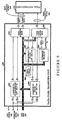
- FIG. 2 illustrates the pattern display system of the currently preferred embodiment of the present invention.
- the multi-channel signal data display apparatus is seen to consist of four pattern display channels 201-204.
- Each channel processes input signal data to convert it to pixel patterns stored in a channel frame buffer.
- the input data is in complex number format so that each data sample represents a vector value. This facilitates the representation of signal magnitude, signal phase, and signal frequency.
- a complex data format is commonly used in current Digital Signal Processing (DSP) systems, digital receivers, and digital data transmission systems. Real digital data can be converted to complex digital data with currently available DSP chips (e.g. Part #GC-1012 available from GrayChip, Inc. of Palo Alto ,California).
- DSP Digital Signal Processing
- the pixel data in each channel frame buffer is read simultaneously to provide screen refresh data to a Pixel Combination Unit (PCU) .
- PCU Pixel Combination Unit
- This unit determines which of the four pixels is displayed, or how individual pixels from each channel are blended to produce single pixels for display monitor 214.
- the resulting pixel stream is fed to a conventional RAMDAC to merge overlay data and to convert 8 bit pixel data to RGB video for the display monitor 214. While the currently preferred embodiment is shown with four channels, different embodiments using more channels, or as few as one channel are possible.
- each pattern is repeated with many cycles to display a long sequence of data values.
- a fixed pixel offset from the root pixel address must be calculated and used for every display pattern cycle after the first cycle.
- the offset required for each pattern cycle is the pixel remainder at the end of the preceding pattern cycle. This pixel remainder must be applied to the next pattern, and this is done using the nearest integer value since only pixel dimensions are involved. In the mathematical calculations however the fractional values must be retained for accuracy. Omission of the offset would cause the signal pattern to be distorted.
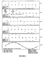
- This process of adding offsets to the root pixel address values is illustrated in Figure 4. Here, the same data shown in Figure 3 is shown with a short pattern cycle of ten data values.
- Pattern 406 Five successive pattern cycles 401-405 are shown with pixel offsets required for patterns 402 through 405. If pixels remain in the frame buffer for five pattern cycles, the composite display will be identical to pattern 302 of Figure 2 (shown here as pattern 406). It should be noted that the number of root pixel addresses used for a pattern cycle is not always the same. Periodically one less pixel address is used, and in the example shown in Figure 4, that occurred during pattern cycle 404. It should also be noted that the offsets are constant for an entire pattern cycle, and changed for each pattern cycle. A following section will describe in more detail how a start pattern address, an end pattern address, and x and y coordinate offsets are used for each pattern cycle. These values, provided by the support computer through the VME bus 113 are required for each pattern cycle. They are also used allow the observer to change the phase of the pattern relative to the data, and to modify the pattern without disturbing the data/pattern phase relationship.
Landscapes
- Engineering & Computer Science (AREA)
- Theoretical Computer Science (AREA)
- Physics & Mathematics (AREA)
- General Physics & Mathematics (AREA)
- Remote Sensing (AREA)
- Computer Hardware Design (AREA)
- Radar, Positioning & Navigation (AREA)
- Human Computer Interaction (AREA)
- Quality & Reliability (AREA)
- General Engineering & Computer Science (AREA)
- Controls And Circuits For Display Device (AREA)
- Control Of Indicators Other Than Cathode Ray Tubes (AREA)
- Testing, Inspecting, Measuring Of Stereoscopic Televisions And Televisions (AREA)
- Television Systems (AREA)
Description
20 offsets and Look-Up Table values. Further, patterns and Look-Up Tables may be stored in the
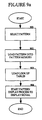
There are numerous changes in the display which may be initiated by the observer. Most often, these changes will be adjustments to the phase of the pattern relative to the incoming data. This is implemented in the associated computer system where a computation of the desired phase shift, based on the observer's inputs using a mouse and keyboard, results in modified start and end addresses for the display cycle which will result in a shift in pattern phase.
Pixel addresses require 11 bits for the horizontal position and 10 bits for the vertical position. The pixel frame buffer address and pixel descriptor word are applied to buffer 609 and subsequently to
During the fifth cycle, four 8 bit pixels from register 707 are applied to
Claims (11)
- A data display system for displaying a plurality of digital data samples of signal data in a predetermined display pattern characteristic of the signal data, said predetermined display pattern being generated by using a preprogrammed root pixel pattern representing root pixel addresses for displaying successive data samples, said data display system comprising:a display monitor (114);a display memory (Frame Buffer FB 208) coupled to said display monitor for storing pixel words for said display monitor;receiving means (Data Input 116) for receiving said plurality of data samples (510);a pixelization means (Data/Pixel Transform Unit DPTU 205) being connected to said receiving means, and storing display values associated with the root pixel pattern, for converting each data sample into a pixel descriptor word (509) describing the pixel shading value (colour; intensity) and the pixel age information of the pixel, and into a pixel address word (508) describing the displacement values (X Axis Data; Y Axis Data) along the x- and the y-axis of the pixel from the corresponding root pixel position as given in the preprogrammed root pixel pattern;a pixel pattern means (pixel pattern unit 206) comprising a pattern storage (604) for storing root pixel addresses of a preprogrammed root pixel pattern, and comprising an offset generator (Horizontal & Vertical Pixel Offsets 603) for computing and storing offset values to root pixel addresses for each cycle of the root pixel pattern which are to be used when the root pixel pattern time is not a multiple of the data sampling interval, and for deriving for each data sample the final data pixel address (X-Axis Address; Y-Axis Address) from the preprogrammed root pixel addresses, the offset values and the displacement values along the x- and y-axis;a pixel aging unit (PAU 207) coupled to the display memory, said pixel aging unit receiving said final data pixel addresses and said pixel descriptor words, and modifying the pixel shading values of said data pixels in said display memory based on predetermined aging criteria.
- The data display system as recited in claim 1, wherein said pixelization means is further comprised of:a first converter to convert said one or more successive data samples to said pixel XY axis displacement value for said data pixel; anda second converter to convert one or more successive data samples to said pixel descriptor word for said data pixel.
- The data display system as recited in claim 2, wherein said offset generator is comprised of:a processing unit to determine a horizontal offset from said root pixel addresses of said pattern and a vertical offset from said root pixel addresses of said pattern for each pattern cycle;a horizontal offset storage coupled to the processing unit to store said horizontal offset; anda vertical offset storage coupled to the processing unit to store said vertical offset.
- The data display system as recited in claim 3, wherein said pixel pattern means is further comprised of:a first summation circuit for generating an X-Axis component of the final data pixel address from an X-Axis component of said root pixel address, a X-Axis component of said displacement value and said horizontal offset; anda second summation circuit for generating an Y-Axis component of the final data pixel address from a Y-Axis component of said root pixel address, a Y-Axis component of said displacement value and said vertical offset.
- The data display system as recited in claim 4, wherein said predetermined aging criteria is comprised of:an aging criteria for controlling each pixel age information; anda shading criteria for controlling pixel shading as a function of said pixel age information.
- The data display system as recited in claim 5, wherein said pixel aging unit is further comprised of:aging means for modifying pixel age information based on said aging criteria; andpixel modification means for modifying pixel shading values based on said shading criteria.
- A method of displaying in a data display system as claimed in Claim 1 a plurality of digital data samples of signal data in a predetermined display pattern characteristic of the signal data, said predetermined display pattern being generated by using a preprogrammed root pixel pattern representing root pixel addresses for displaying successive data samples, said method comprising the steps of:a. generating and storing root pixel addresses of a preprogrammed root pixel pattern, and display values associated with the root pixel pattern, and offset values to root pixel addresses being computed for each cycle of the root pattern and being used when the pattern time is not a multiple of the data sampling interval;b. receiving said plurality of data samples;c. converting a data sample of said plurality of data samples by means of said display values into a pixel descriptor word (509) describing the pixel shading value (colour; intensity) and the pixel age information of the pixel, and into a pixel address word (508) describing the displacement values (X Axis Data; Y Axis Data) along the x- and the y-axis of the pixel from the corresponding root pixel position as given in the preprogrammed root pixel pattern;d. deriving for said data sample the final data pixel addresses (X-Axis Address; Y-Axis Address) from the preprogrammed root pixel addresses, the offset value and the displacement values along the x- and y-axis;e. receiving and storing said final data pixel addresses and said pixel descriptor word in a display memory, and modifying the pixel shading value of said data pixel based on predetermined aging criteria;f. repeating steps c to e for each root pixel address of said preprogrammed root pixel pattern;g. repeating steps b to f for a new incoming plurality of data samples.
- The method as recited in claim 7, said method is further comprised of the steps of:i) retrieving one or more pixel shading values from said display memory;
for each of said retrieved one or more pixel shading values;k1) examining pixel aging information of said one or more pixel shading values;k2) aging said one or more pixels by modifying said pixel aging information;k3) modifying said pixel shading value according to a predetermined pixel aging criteria; and1) storing said one or more pixel shading values back into said display memory. - The method as recited in claim 8, wherein said step of loading said pattern and display values into a pattern display system is further comprised of the steps of:a) loading said pattern into a pattern storage; andb) loading said display values into a pixel shading look-up table and into a pixel XY axis displacement look-up table.
- The method as recited in claim 9, wherein said step of generating a pixel address for said data sample based on said pattern and said offset is further comprised of the steps of:a) providing said data sample to said pixel XY axis displacement look-up table, and outputting the pixel XY axis displacement value;b) retrieving a successive root pixel address from said pattern memory; andc) combining said successive root pixel address with said offset and said pixel XY axis displacement value to create said pixel address.
- The method as recited in claim 10, wherein said step of generating a pixel shading value for said signal sample is further comprised of the steps of:a) generating polar coordinates from said data sample;b) providing said XY magnitude and said polar coordinates to said look-up table; andc) outputting a corresponding pixel shading value from said look-up table.
Applications Claiming Priority (3)
| Application Number | Priority Date | Filing Date | Title |
|---|---|---|---|
| US95661 | 1993-07-21 | ||
| US08/095,661 US5479606A (en) | 1993-07-21 | 1993-07-21 | Data display apparatus for displaying patterns using samples of signal data |
| PCT/US1994/007939 WO1995003585A1 (en) | 1993-07-21 | 1994-07-15 | A data display apparatus for displaying digital samples of signal data on a bit mapped display system |
Publications (3)
| Publication Number | Publication Date |
|---|---|
| EP0710377A1 EP0710377A1 (en) | 1996-05-08 |
| EP0710377A4 EP0710377A4 (en) | 1997-04-09 |
| EP0710377B1 true EP0710377B1 (en) | 2001-09-26 |
Family
ID=22253030
Family Applications (1)
| Application Number | Title | Priority Date | Filing Date |
|---|---|---|---|
| EP94923493A Expired - Lifetime EP0710377B1 (en) | 1993-07-21 | 1994-07-15 | A data display apparatus and method for displaying digital samples of signal data on a bit mapped display system |
Country Status (6)
| Country | Link |
|---|---|
| US (2) | US5479606A (en) |
| EP (1) | EP0710377B1 (en) |
| AU (1) | AU680026B2 (en) |
| CA (1) | CA2167689C (en) |
| DE (1) | DE69428447T2 (en) |
| WO (1) | WO1995003585A1 (en) |
Families Citing this family (51)
| Publication number | Priority date | Publication date | Assignee | Title |
|---|---|---|---|---|
| US5479606A (en) * | 1993-07-21 | 1995-12-26 | Pgm Systems, Inc. | Data display apparatus for displaying patterns using samples of signal data |
| DE4433953A1 (en) * | 1994-09-23 | 1996-03-28 | Bosch Gmbh Robert | Procedure for displaying information on a screen |
| US5668941A (en) * | 1995-06-22 | 1997-09-16 | Cirrus Logic, Inc. | Optimum implementation of X-Y clipping on pixel boundary |
| DE19547896C2 (en) * | 1995-12-21 | 1999-12-23 | Rohde & Schwarz | Arrangement for displaying the signal states of a QAM-modulated signal |
| US5812112A (en) * | 1996-03-27 | 1998-09-22 | Fluke Corporation | Method and system for building bit plane images in bit-mapped displays |
| US6812930B1 (en) * | 1996-05-10 | 2004-11-02 | Apple Computer, Inc. | Transparent compatibility and adaptation to differing format implementations in a computer system |
| US6025829A (en) * | 1996-10-28 | 2000-02-15 | Welch Allyn, Inc. | Image generator for video display |
| JP3052891B2 (en) * | 1997-05-26 | 2000-06-19 | 日本電気株式会社 | Signal processing system |
| US6798420B1 (en) * | 1998-11-09 | 2004-09-28 | Broadcom Corporation | Video and graphics system with a single-port RAM |
| US6636222B1 (en) | 1999-11-09 | 2003-10-21 | Broadcom Corporation | Video and graphics system with an MPEG video decoder for concurrent multi-row decoding |
| US6573905B1 (en) | 1999-11-09 | 2003-06-03 | Broadcom Corporation | Video and graphics system with parallel processing of graphics windows |
| US7982740B2 (en) | 1998-11-09 | 2011-07-19 | Broadcom Corporation | Low resolution graphics mode support using window descriptors |
| US6661422B1 (en) | 1998-11-09 | 2003-12-09 | Broadcom Corporation | Video and graphics system with MPEG specific data transfer commands |
| US6768774B1 (en) | 1998-11-09 | 2004-07-27 | Broadcom Corporation | Video and graphics system with video scaling |
| US6738072B1 (en) * | 1998-11-09 | 2004-05-18 | Broadcom Corporation | Graphics display system with anti-flutter filtering and vertical scaling feature |
| US7446774B1 (en) | 1998-11-09 | 2008-11-04 | Broadcom Corporation | Video and graphics system with an integrated system bridge controller |
| US6853385B1 (en) | 1999-11-09 | 2005-02-08 | Broadcom Corporation | Video, audio and graphics decode, composite and display system |
| US6975324B1 (en) | 1999-11-09 | 2005-12-13 | Broadcom Corporation | Video and graphics system with a video transport processor |
| US6980212B2 (en) * | 2001-04-17 | 2005-12-27 | Tektronix, Inc. | Method and apparatus for computing thresholds for identification of waveform anomalies |
| US7019746B2 (en) * | 2001-10-26 | 2006-03-28 | Agilent Technologies, Inc. | Graphical presentation of spectral information for aid in compliance measurements |
| US7076093B2 (en) * | 2002-09-16 | 2006-07-11 | Lee Shih-Jong J | Structure-guided image inspection |
| US8063916B2 (en) | 2003-10-22 | 2011-11-22 | Broadcom Corporation | Graphics layer reduction for video composition |
| EP2383721B1 (en) * | 2004-11-16 | 2015-04-08 | Ignis Innovation Inc. | System and Driving Method for Active Matrix Light Emitting Device Display |
| CA2490858A1 (en) | 2004-12-07 | 2006-06-07 | Ignis Innovation Inc. | Driving method for compensated voltage-programming of amoled displays |
| CN102663977B (en) * | 2005-06-08 | 2015-11-18 | 伊格尼斯创新有限公司 | For driving the method and system of light emitting device display |
| US9489891B2 (en) | 2006-01-09 | 2016-11-08 | Ignis Innovation Inc. | Method and system for driving an active matrix display circuit |
| WO2007079572A1 (en) | 2006-01-09 | 2007-07-19 | Ignis Innovation Inc. | Method and system for driving an active matrix display circuit |
| US9269322B2 (en) | 2006-01-09 | 2016-02-23 | Ignis Innovation Inc. | Method and system for driving an active matrix display circuit |
| TW200949807A (en) | 2008-04-18 | 2009-12-01 | Ignis Innovation Inc | System and driving method for light emitting device display |
| CA2637343A1 (en) | 2008-07-29 | 2010-01-29 | Ignis Innovation Inc. | Improving the display source driver |
| US9370075B2 (en) | 2008-12-09 | 2016-06-14 | Ignis Innovation Inc. | System and method for fast compensation programming of pixels in a display |
| US8633873B2 (en) | 2009-11-12 | 2014-01-21 | Ignis Innovation Inc. | Stable fast programming scheme for displays |
| CA2687631A1 (en) | 2009-12-06 | 2011-06-06 | Ignis Innovation Inc | Low power driving scheme for display applications |
| CA2696778A1 (en) | 2010-03-17 | 2011-09-17 | Ignis Innovation Inc. | Lifetime, uniformity, parameter extraction methods |
| US9351368B2 (en) | 2013-03-08 | 2016-05-24 | Ignis Innovation Inc. | Pixel circuits for AMOLED displays |
| US20140368491A1 (en) | 2013-03-08 | 2014-12-18 | Ignis Innovation Inc. | Pixel circuits for amoled displays |
| US9886899B2 (en) | 2011-05-17 | 2018-02-06 | Ignis Innovation Inc. | Pixel Circuits for AMOLED displays |
| EP2715711A4 (en) | 2011-05-28 | 2014-12-24 | Ignis Innovation Inc | System and method for fast compensation programming of pixels in a display |
| US9747834B2 (en) | 2012-05-11 | 2017-08-29 | Ignis Innovation Inc. | Pixel circuits including feedback capacitors and reset capacitors, and display systems therefore |
| US9786223B2 (en) | 2012-12-11 | 2017-10-10 | Ignis Innovation Inc. | Pixel circuits for AMOLED displays |
| US9336717B2 (en) | 2012-12-11 | 2016-05-10 | Ignis Innovation Inc. | Pixel circuits for AMOLED displays |
| CA2894717A1 (en) | 2015-06-19 | 2016-12-19 | Ignis Innovation Inc. | Optoelectronic device characterization in array with shared sense line |
| US9721505B2 (en) | 2013-03-08 | 2017-08-01 | Ignis Innovation Inc. | Pixel circuits for AMOLED displays |
| US12469041B2 (en) | 2014-05-02 | 2025-11-11 | Tillster, Inc. | Mobile loyalty and payment system using temporary short codes |
| CA2873476A1 (en) | 2014-12-08 | 2016-06-08 | Ignis Innovation Inc. | Smart-pixel display architecture |
| CA2886862A1 (en) | 2015-04-01 | 2016-10-01 | Ignis Innovation Inc. | Adjusting display brightness for avoiding overheating and/or accelerated aging |
| US10657895B2 (en) | 2015-07-24 | 2020-05-19 | Ignis Innovation Inc. | Pixels and reference circuits and timing techniques |
| US10373554B2 (en) | 2015-07-24 | 2019-08-06 | Ignis Innovation Inc. | Pixels and reference circuits and timing techniques |
| CA2898282A1 (en) | 2015-07-24 | 2017-01-24 | Ignis Innovation Inc. | Hybrid calibration of current sources for current biased voltage progra mmed (cbvp) displays |
| CA2908285A1 (en) | 2015-10-14 | 2017-04-14 | Ignis Innovation Inc. | Driver with multiple color pixel structure |
| KR102795159B1 (en) * | 2020-12-15 | 2025-04-14 | 엘지디스플레이 주식회사 | Electroluminescence Display Device And Driving Method Thereof |
Family Cites Families (13)
| Publication number | Priority date | Publication date | Assignee | Title |
|---|---|---|---|---|
| CN1012301B (en) * | 1984-10-16 | 1991-04-03 | 三洋电机株式会社 | display device |
| US4829293A (en) * | 1985-05-06 | 1989-05-09 | Hewlett-Packard Company | Method and apparatus for achieving variable and infinite persistence |
| US4933878A (en) * | 1988-07-07 | 1990-06-12 | Texas Instruments Incorporated | Graphics data processing apparatus having non-linear saturating operations on multibit color data |
| JPH0812705B2 (en) * | 1986-09-29 | 1996-02-07 | 株式会社東芝 | Image processing device |
| US4766425A (en) * | 1986-12-19 | 1988-08-23 | Tektronix, Inc. | Waveform selection by touch |
| JPS63204595A (en) * | 1987-02-20 | 1988-08-24 | Fujitsu Ltd | Multi-plane video ram constituting system |
| US4977514A (en) * | 1987-05-08 | 1990-12-11 | Hewlett Packard Company | Overlaid digital waveforms display |
| GB2214764B (en) * | 1988-01-29 | 1992-01-08 | Tektronix Inc | Pixel intensity modulation in a waveform display |
| US4974167A (en) * | 1989-02-28 | 1990-11-27 | Tektronix, Inc. | Erasable data acquisition and storage instrument |
| US5739807A (en) * | 1991-09-13 | 1998-04-14 | Tektronix, Inc. | Method for presenting complex number waveforms |
| US5274760A (en) * | 1991-12-24 | 1993-12-28 | International Business Machines Corporation | Extendable multiple image-buffer for graphics systems |
| US5367632A (en) * | 1992-10-30 | 1994-11-22 | International Business Machines Corporation | Flexible memory controller for graphics applications |
| US5479606A (en) * | 1993-07-21 | 1995-12-26 | Pgm Systems, Inc. | Data display apparatus for displaying patterns using samples of signal data |
-
1993
- 1993-07-21 US US08/095,661 patent/US5479606A/en not_active Expired - Lifetime
-
1994
- 1994-07-15 CA CA002167689A patent/CA2167689C/en not_active Expired - Fee Related
- 1994-07-15 AU AU73344/94A patent/AU680026B2/en not_active Ceased
- 1994-07-15 EP EP94923493A patent/EP0710377B1/en not_active Expired - Lifetime
- 1994-07-15 WO PCT/US1994/007939 patent/WO1995003585A1/en not_active Ceased
- 1994-07-15 DE DE69428447T patent/DE69428447T2/en not_active Expired - Fee Related
-
1995
- 1995-12-22 US US08/577,336 patent/US5758129A/en not_active Expired - Lifetime
Also Published As
| Publication number | Publication date |
|---|---|
| EP0710377A4 (en) | 1997-04-09 |
| CA2167689C (en) | 2002-04-23 |
| EP0710377A1 (en) | 1996-05-08 |
| AU7334494A (en) | 1995-02-20 |
| US5479606A (en) | 1995-12-26 |
| DE69428447T2 (en) | 2002-05-29 |
| CA2167689A1 (en) | 1995-02-02 |
| DE69428447D1 (en) | 2001-10-31 |
| WO1995003585A1 (en) | 1995-02-02 |
| US5758129A (en) | 1998-05-26 |
| AU680026B2 (en) | 1997-07-17 |
Similar Documents
| Publication | Publication Date | Title |
|---|---|---|
| EP0710377B1 (en) | A data display apparatus and method for displaying digital samples of signal data on a bit mapped display system | |
| US4524421A (en) | Computerized graphics system and method using an electronically synthesized palette | |
| US4954970A (en) | Video overlay image processing apparatus | |
| EP0403054B1 (en) | An electronic graphic system | |
| JP3452616B2 (en) | Multi-resolution image display method and apparatus | |
| US5260695A (en) | Color map image fader for graphics window subsystem | |
| US6181353B1 (en) | On-screen display device using horizontal scan line memories | |
| EP0947955A2 (en) | Methods and apparatus for generating custom gamma curves for color correction equipment | |
| US7768533B2 (en) | Video generator with NTSC/PAL conversion capability | |
| JPS61148488A (en) | display control device | |
| JPH021894A (en) | Method and apparatus for generating color characteristic of object | |
| US5874991A (en) | Apparatus for the creation of video test signals | |
| US6396536B1 (en) | Automatic test instrument for multi-format video generation and capture | |
| US4625202A (en) | Apparatus and method for generating multiple cursors in a raster scan display system | |
| US20030189581A1 (en) | Content based window filtering for simultaneous display of multiple high-quality video and graphics windows | |
| US4872001A (en) | Split screen imaging | |
| EP0599936A1 (en) | High speed ramdac with reconfigurable color palette | |
| US20050093978A1 (en) | Video generation and capture techniques | |
| JPS6191777A (en) | Video image forming apparatus | |
| EP0371231B1 (en) | Method and apparatus for increasing image generation speed on raster displays | |
| EP0202747A2 (en) | Improvements in or relating to video image creation systems | |
| US4945497A (en) | Method and apparatus for translating rectilinear information into scan line information for display by a computer system | |
| US5359545A (en) | Dynamic video display for logic simulation systems | |
| US5592196A (en) | Picture data processing apparatus | |
| EP0441499A2 (en) | Electronic brush generation |
Legal Events
| Date | Code | Title | Description |
|---|---|---|---|
| PUAI | Public reference made under article 153(3) epc to a published international application that has entered the european phase |
Free format text: ORIGINAL CODE: 0009012 |
|
| 17P | Request for examination filed |
Effective date: 19960219 |
|
| AK | Designated contracting states |
Kind code of ref document: A1 Designated state(s): DE FR GB IT |
|
| A4 | Supplementary search report drawn up and despatched |
Effective date: 19970225 |
|
| AK | Designated contracting states |
Kind code of ref document: A4 Designated state(s): DE FR GB IT |
|
| 17Q | First examination report despatched |
Effective date: 19990723 |
|
| RIC1 | Information provided on ipc code assigned before grant |
Free format text: 7G 06F 11/32 A, 7G 09G 1/16 B |
|
| RTI1 | Title (correction) |
Free format text: A DATA DISPLAY APPARATUS AND METHOD FOR DISPLAYING DIGITAL SAMPLES OF SIGNAL DATA ON A BIT MAPPED DISPLAY SYSTEM |
|
| GRAG | Despatch of communication of intention to grant |
Free format text: ORIGINAL CODE: EPIDOS AGRA |
|
| GRAG | Despatch of communication of intention to grant |
Free format text: ORIGINAL CODE: EPIDOS AGRA |
|
| GRAH | Despatch of communication of intention to grant a patent |
Free format text: ORIGINAL CODE: EPIDOS IGRA |
|
| GRAH | Despatch of communication of intention to grant a patent |
Free format text: ORIGINAL CODE: EPIDOS IGRA |
|
| GRAA | (expected) grant |
Free format text: ORIGINAL CODE: 0009210 |
|
| AK | Designated contracting states |
Kind code of ref document: B1 Designated state(s): DE FR GB IT |
|
| REF | Corresponds to: |
Ref document number: 69428447 Country of ref document: DE Date of ref document: 20011031 |
|
| REG | Reference to a national code |
Ref country code: GB Ref legal event code: IF02 |
|
| ET | Fr: translation filed | ||
| PLBE | No opposition filed within time limit |
Free format text: ORIGINAL CODE: 0009261 |
|
| STAA | Information on the status of an ep patent application or granted ep patent |
Free format text: STATUS: NO OPPOSITION FILED WITHIN TIME LIMIT |
|
| 26N | No opposition filed | ||
| PGFP | Annual fee paid to national office [announced via postgrant information from national office to epo] |
Ref country code: FR Payment date: 20090717 Year of fee payment: 16 |
|
| PGFP | Annual fee paid to national office [announced via postgrant information from national office to epo] |
Ref country code: GB Payment date: 20090727 Year of fee payment: 16 Ref country code: DE Payment date: 20090729 Year of fee payment: 16 |
|
| PGFP | Annual fee paid to national office [announced via postgrant information from national office to epo] |
Ref country code: IT Payment date: 20090730 Year of fee payment: 16 |
|
| GBPC | Gb: european patent ceased through non-payment of renewal fee |
Effective date: 20100715 |
|
| REG | Reference to a national code |
Ref country code: FR Ref legal event code: ST Effective date: 20110331 |
|
| PG25 | Lapsed in a contracting state [announced via postgrant information from national office to epo] |
Ref country code: DE Free format text: LAPSE BECAUSE OF NON-PAYMENT OF DUE FEES Effective date: 20110201 |
|
| REG | Reference to a national code |
Ref country code: DE Ref legal event code: R119 Ref document number: 69428447 Country of ref document: DE Effective date: 20110201 |
|
| PG25 | Lapsed in a contracting state [announced via postgrant information from national office to epo] |
Ref country code: IT Free format text: LAPSE BECAUSE OF NON-PAYMENT OF DUE FEES Effective date: 20100715 Ref country code: FR Free format text: LAPSE BECAUSE OF NON-PAYMENT OF DUE FEES Effective date: 20100802 |
|
| PG25 | Lapsed in a contracting state [announced via postgrant information from national office to epo] |
Ref country code: GB Free format text: LAPSE BECAUSE OF NON-PAYMENT OF DUE FEES Effective date: 20100715 |