EP0710001B1 - A fuzzy logic filter for images with impulse noise - Google Patents
A fuzzy logic filter for images with impulse noise Download PDFInfo
- Publication number
- EP0710001B1 EP0710001B1 EP94830521A EP94830521A EP0710001B1 EP 0710001 B1 EP0710001 B1 EP 0710001B1 EP 94830521 A EP94830521 A EP 94830521A EP 94830521 A EP94830521 A EP 94830521A EP 0710001 B1 EP0710001 B1 EP 0710001B1
- Authority
- EP
- European Patent Office
- Prior art keywords
- filter
- accordance
- digital
- output
- block
- Prior art date
- Legal status (The legal status is an assumption and is not a legal conclusion. Google has not performed a legal analysis and makes no representation as to the accuracy of the status listed.)
- Expired - Lifetime
Links
- 238000000034 method Methods 0.000 claims description 19
- 238000001914 filtration Methods 0.000 claims description 16
- 230000000694 effects Effects 0.000 description 3
- 238000001514 detection method Methods 0.000 description 1
- 238000012986 modification Methods 0.000 description 1
- 230000004048 modification Effects 0.000 description 1
Images


Classifications
-
- G—PHYSICS
- G06—COMPUTING; CALCULATING OR COUNTING
- G06T—IMAGE DATA PROCESSING OR GENERATION, IN GENERAL
- G06T5/00—Image enhancement or restoration
- G06T5/20—Image enhancement or restoration using local operators
-
- H—ELECTRICITY
- H03—ELECTRONIC CIRCUITRY
- H03H—IMPEDANCE NETWORKS, e.g. RESONANT CIRCUITS; RESONATORS
- H03H2222/00—Indexing scheme relating to digital filtering methods
- H03H2222/02—Indexing scheme relating to digital filtering methods using fuzzy logic
Definitions
- the present invention relates to an electronic device used in video applications and specifically to a filter performing on video images a reduction of the pulsed noise in accordance with fuzzy logic.
- the present invention also relates to a method for performing on video images a reduction of the pulsed noise in accordance with fuzzy logic.
- a typical noise present in video signals is the pulsed noise. Its effects are such as to change the grey level of a so-called image pixel so as to cause a peak of luminosity (positive or negative) to appear in a nearly homogeneous image region.
- the technical problem underlying the present invention is to provide a filter and associated filtering method for performing a reduction of the pulsed noise contained in video images in accordance with fuzzy logic which would be structurally very simple while achieving high quality of the filtered image.
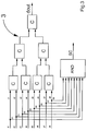
- the number 1 indicates schematically as a whole a filter provided in accordance with the present invention to secure reduction of the pulsed noise on video images and in accordance with a fuzzy logic procedure.
- image field is defined as a group of lines constituting a video image in the same time interval.
- the filter 1 has at least three input terminals designed to receive digital signals for image lines consecutive in time CF_PPL, CF_PL, CF_CL of a current image field.
- the filter 1 comprises an interface circuit 2 having a first, a second and a third input terminal coinciding with the input terminals of the filter 1, and a plurality of output terminals.
- FIG. 2 shows in greater detail the internal structure of the interface circuit 2.
- It comprises a plurality of delay blocks T which allow delaying appropriately the digital signals present at the inputs of the filter 1 so as to create a working window or image window shown in FIG. 2A.
- this window comprises nine digital signals.
- the digital signals included in the central line belong to the image line CF_PL while the digital signals included in the first and last lines belong to the image lines CF_PPL and CF_CL.
- the digital signal X in which the work signal is centred is the signal to be processed.
- SDi digital subtractors
- the first input terminals of the digital subtractors SDi are designed to receive the digital signal X to be processed while each of the second input terminals of said subtractors receives one of the remaining digital signals included in the image window.
- each of the signals di represent the difference between the grey level associated with the image pixel to be processed and the grey level associated with an image pixel adjacent thereto.
- a pixel is considered affected by pulsed noise if its grey level is totally different from the grey level of the pixels adjacent thereto.
- the filter 1 also comprises a comparator block 3 whose internal structure is shown in FIG. 3 which has a plurality of input terminals designed to receive the difference signals di and a first and a second output terminal.
- This comparator block 3 is designed to perform on said difference signals di subsequent comparisons by means of a plurality of comparator sub-blocks C connected together in cascade.
- the first output terminal of block 3 receives a difference signal dout coinciding with that between the difference signals di which has minimum modulus value.
- the difference signals di are coded with six bits of which the most (or least) significant represents the sign.
- Said logic circuit L is provided essentially through an AND logic port with eight inputs and is designed to generate a control signal SC which is received from the second output terminal of block 3.
- the signal SC can assume the logic values 0 or 1.
- the filter 1 comprises a memory circuit 4 having a first input terminal connected to the first output terminal dout of the comparator block 3 and of an output terminal.
- the circuit 4 also has an enablement input designed to receive the control signal SC present at the output of the logic circuit L.
- control signal SC assumes value 0, i.e. the difference signals di do not all exhibit the same sign, the pixel being processed is surely not affected by pulsed noise because its grey level is not totally different from the grey levels of the adjacent pixels.
- the pixel being processed is not filtered.
- control signal SC assumes value 1 the pixel being processed may or may not be affected by pulsed noise.
- the memory circuit 4 comprises a plurality of memory elements addressed through the value of dout and designed for memorising the results achieved by executing off-line a fuzzy procedure, which is described below, to appraise in what measure the pixel being processed is affected or not by pulsed noise.
- Said results represent the values, inside the interval [0,1], taken on by a Knoise parameter which is representative of the quantity of pulsed noise present in the pixel being processed.
- the structure of the filter 1 also comprises an arithmetic block 5 having a first, a second and a third input terminal and an output terminal coinciding with an output terminal of the filter 1.
- a filtering circuit F having a first, a second and a third input terminal and an output terminal.
- the first input terminal of the arithmetic block 5 is connected to the output terminal of the memory circuit 4 while the second and third input terminals of said block are connected to the third input terminal and the output terminal respectively of the filtering circuit F.
- the input terminals of the circuit F are connected to output terminals of the interface circuit 2 so as to receive the digital signals P7, P2 and X respectively situated along a column of the image window.
- the filtering circuit F whose embodiment calls for the employment of a vertical median filter with three points of the conventional type is designed to organize the values of the signals present at its inputs and supply at output a value indicated by M.
- the filtering method is essentially structured in accordance with two successive steps.
- the filter 1 through the formula (1) implemented by the arithmetic block 5 performs a soft switch between the original digital signal X representing the grey level associated with the pixel being processed and the output M of the filtering circuit F.
- each rule includes at least eight antecedent prepositions each represented by a difference signal di calculated through the digital subtractors SDi.
- Calculation of the antecedent part of the fuzzy rules through the comparator block 3 produces as a result a value for the digital signal dout.
Landscapes
- Physics & Mathematics (AREA)
- General Physics & Mathematics (AREA)
- Engineering & Computer Science (AREA)
- Theoretical Computer Science (AREA)
- Picture Signal Circuits (AREA)
- Image Processing (AREA)
Description
Claims (9)
- Filter for performing a reduction of pulsed noise on video images in accordance with fuzzy logic, comprising:at least one interface circuit (2) receiving as input digital signals consecutive in time and corresponding to said video images and designed to generate an image window centred in a digital signal (X) to be processed,at least one comparator block (3) having a plurality of input terminals coupled with output terminals of the interface circuit (2) through a plurality of digital subtractors (SDi),at least one memory circuit (4) connected in cascade with the comparator block (3) and comprising a plurality of memory elements designed to store values of a parameter (Knoise) obtained from a procedure performed by fuzzy logic procedures on the basis of outputs of the comparator block (3),at least one filtering circuit (F) having inputs connected to some outputs of the interface circuit (2) and designed to organize the values of said inputs,at least one arithmetic block (5) having a first input terminal connected to an output terminal of the memory circuit (4) and a second input terminal designed to receive the digital signal (X) to be processed and a third input terminal connected to an output terminal of the filtering circuit (F) and said arithmetic block (5) being designed to perform a switch between the digital signal (X) to be processed and the output of the filtering circuit (F) on the basis of the values taken by the parameter (Knoise).
- Filter in accordance with claim 1 characterised in that the comparator block (3) comprises a plurality of comparator sub-blocks (C) of which some are connected at output to the digital subtractors (SDi) and the remaining ones connected together in cascade and which are designed to perform subsequent comparisons on difference signals (di), calculated by the digital subtractors (SDi), to generate a difference signal (dout) having minimal modulus.
- Filter in accordance with claim 2 characterised in that the comparator block (3) comprises a logic block (L) having a plurality of input terminals each connected to the output of a corresponding digital subtractor (SDi) to receive digital signals (Si) representing the sign bit of the difference signals (di) and said logic block (L) being designed to generate a control signal (SC).
- Filter in accordance with claim 3 characterised in that said control signal (SC) is received by an enablement input of the memory circuit (4).
- Filter in accordance with claim 3 characterised in that said logic block (L) is provided through an AND logical gate.
- Filter in accordance with claim 4 characterised in that the plurality of memory elements included in the memory circuit (4) are addressed through the digital signal (dout) output from the comparator block (3).
- Method of filtering the pulsed noise present in video images for which is defined an image window centred in a digital signal (X) to be processed through an interface circuit (2) and said digital signal (X) to be processed being filtered in a filtering circuit (F), comprising at least the steps ofdetecting on the basis of fuzzy logic procedures parameter values (Knoise) for use in an interpolation arithmetic block (5), andswitching on the basis of the values of the parameter (Knoise) between a digital signal (X) to be processed and the output of the filtering circuit (F).
- Method in accordance with claim 7 characterised in that the detecting step comprises a comparison between the digital signal (X) to be processed and other digital signals included in the image window obtained by means of the interface circuit (2).
- Method in accordance with claim 8 characterised in that said comparison is performed through a comparator block (3) having a plurality of input terminals coupled with output terminals of the interface circuit (2) through a plurality of subtractors (Sdi).
Priority Applications (4)
| Application Number | Priority Date | Filing Date | Title |
|---|---|---|---|
| EP94830521A EP0710001B1 (en) | 1994-10-31 | 1994-10-31 | A fuzzy logic filter for images with impulse noise |
| DE69417236T DE69417236T2 (en) | 1994-10-31 | 1994-10-31 | Fuzzy logic filter for images with impulse noise |
| US08/558,596 US6034741A (en) | 1994-10-31 | 1995-10-30 | Fuzzy logic filter for impulsive noisy images |
| JP7283369A JPH08275031A (en) | 1994-10-31 | 1995-10-31 | Filter for pulsation noise reduction of video picture |
Applications Claiming Priority (1)
| Application Number | Priority Date | Filing Date | Title |
|---|---|---|---|
| EP94830521A EP0710001B1 (en) | 1994-10-31 | 1994-10-31 | A fuzzy logic filter for images with impulse noise |
Publications (2)
| Publication Number | Publication Date |
|---|---|
| EP0710001A1 EP0710001A1 (en) | 1996-05-01 |
| EP0710001B1 true EP0710001B1 (en) | 1999-03-17 |
Family
ID=8218569
Family Applications (1)
| Application Number | Title | Priority Date | Filing Date |
|---|---|---|---|
| EP94830521A Expired - Lifetime EP0710001B1 (en) | 1994-10-31 | 1994-10-31 | A fuzzy logic filter for images with impulse noise |
Country Status (4)
| Country | Link |
|---|---|
| US (1) | US6034741A (en) |
| EP (1) | EP0710001B1 (en) |
| JP (1) | JPH08275031A (en) |
| DE (1) | DE69417236T2 (en) |
Cited By (1)
| Publication number | Priority date | Publication date | Assignee | Title |
|---|---|---|---|---|
| CZ304181B6 (en) * | 2009-02-16 | 2013-12-11 | Vysoké ucení technické v Brne, Fakulta informacních technologií | Non-linear video filter |
Families Citing this family (3)
| Publication number | Priority date | Publication date | Assignee | Title |
|---|---|---|---|---|
| EP0794512B1 (en) * | 1996-03-07 | 2002-08-28 | STMicroelectronics S.r.l. | Processing device for video signals |
| KR100446723B1 (en) * | 1997-10-23 | 2004-11-16 | 엘지전자 주식회사 | Method for removing noise from a gray image by mathematically optimizing properties of an image consisting of a small number of gray levels |
| JP5120441B2 (en) * | 2009-11-26 | 2013-01-16 | 株式会社ニコン | Image processing device |
Family Cites Families (6)
| Publication number | Priority date | Publication date | Assignee | Title |
|---|---|---|---|---|
| EP0415648B1 (en) * | 1989-08-31 | 1998-05-20 | Canon Kabushiki Kaisha | Image processing apparatus |
| JPH04294466A (en) * | 1991-03-22 | 1992-10-19 | Ricoh Co Ltd | Image processor |
| JPH0591532A (en) * | 1991-09-30 | 1993-04-09 | Toshiba Corp | Image filter and adaptive type image filter learning method |
| JPH0594523A (en) * | 1991-10-01 | 1993-04-16 | Yokogawa Medical Syst Ltd | Method and device for processing image |
| EP0655711B1 (en) * | 1993-11-30 | 2000-03-29 | STMicroelectronics S.r.l. | Filter working on image digital signals for video appliances |
| DE69431707D1 (en) * | 1994-04-27 | 2002-12-19 | Sgs Thomson Microelectronics | Noise-reducing filtering and interpolating sample rate conversion for digital video signals, controlled by inter-field correlation information detected with fuzzy logic |
-
1994
- 1994-10-31 DE DE69417236T patent/DE69417236T2/en not_active Expired - Fee Related
- 1994-10-31 EP EP94830521A patent/EP0710001B1/en not_active Expired - Lifetime
-
1995
- 1995-10-30 US US08/558,596 patent/US6034741A/en not_active Expired - Lifetime
- 1995-10-31 JP JP7283369A patent/JPH08275031A/en active Pending
Cited By (1)
| Publication number | Priority date | Publication date | Assignee | Title |
|---|---|---|---|---|
| CZ304181B6 (en) * | 2009-02-16 | 2013-12-11 | Vysoké ucení technické v Brne, Fakulta informacních technologií | Non-linear video filter |
Also Published As
| Publication number | Publication date |
|---|---|
| EP0710001A1 (en) | 1996-05-01 |
| DE69417236D1 (en) | 1999-04-22 |
| DE69417236T2 (en) | 1999-07-08 |
| US6034741A (en) | 2000-03-07 |
| JPH08275031A (en) | 1996-10-18 |
Similar Documents
| Publication | Publication Date | Title |
|---|---|---|
| US4682230A (en) | Adaptive median filter system | |
| JP2565315B2 (en) | Motion detection circuit | |
| US3973239A (en) | Pattern preliminary processing system | |
| US4982354A (en) | Digital finite impulse response filter and method | |
| US5757977A (en) | Fuzzy logic filter for reducing noise and sharpening edges of digital image signals | |
| EP0782319B1 (en) | Apparatus for symmetrically reducing "N" least significant bits of an M-Bit digital signal | |
| US5867228A (en) | Video signal noise reduction apparatus with variable S/N improving amount | |
| EP0114961B1 (en) | Nonlinear filtering of gray scale video images | |
| EP0710001B1 (en) | A fuzzy logic filter for images with impulse noise | |
| EP0680224A1 (en) | Fuzzy logic based filter architecture for video applications and corresponding filtering method | |
| EP0079175B1 (en) | Boolean filtering method and apparatus | |
| JPH06276392A (en) | Picture processing unit | |
| EP1396081B1 (en) | Two-dimensional pyramid filter architecture | |
| EP0655711B1 (en) | Filter working on image digital signals for video appliances | |
| EP1169868B1 (en) | Method of reducing blocking artifacts | |
| JP3533697B2 (en) | Adaptive filter device and adaptive filter processing method | |
| JPS60128791A (en) | Circuit for detecting movement of video signal | |
| EP0368671A3 (en) | Feature extracting apparatus | |
| KR100317674B1 (en) | Recursive noise reduction system | |
| JP2585872B2 (en) | Image noise removal device | |
| KR960013221B1 (en) | Video signal transition region emphasizing apparatus | |
| SU1529262A1 (en) | Device for processing images of objects | |
| JP2565177B2 (en) | Noise removal circuit | |
| JPS61290867A (en) | Image input device | |
| JPH0225223B2 (en) |
Legal Events
| Date | Code | Title | Description |
|---|---|---|---|
| PUAI | Public reference made under article 153(3) epc to a published international application that has entered the european phase |
Free format text: ORIGINAL CODE: 0009012 |
|
| AK | Designated contracting states |
Kind code of ref document: A1 Designated state(s): DE FR GB IT |
|
| 17P | Request for examination filed |
Effective date: 19961021 |
|
| RAP3 | Party data changed (applicant data changed or rights of an application transferred) |
Owner name: STMICROELECTRONICS S.R.L. |
|
| GRAG | Despatch of communication of intention to grant |
Free format text: ORIGINAL CODE: EPIDOS AGRA |
|
| GRAH | Despatch of communication of intention to grant a patent |
Free format text: ORIGINAL CODE: EPIDOS IGRA |
|
| 17Q | First examination report despatched |
Effective date: 19980713 |
|
| GRAH | Despatch of communication of intention to grant a patent |
Free format text: ORIGINAL CODE: EPIDOS IGRA |
|
| GRAA | (expected) grant |
Free format text: ORIGINAL CODE: 0009210 |
|
| AK | Designated contracting states |
Kind code of ref document: B1 Designated state(s): DE FR GB IT |
|
| REF | Corresponds to: |
Ref document number: 69417236 Country of ref document: DE Date of ref document: 19990422 |
|
| ET | Fr: translation filed | ||
| PLBE | No opposition filed within time limit |
Free format text: ORIGINAL CODE: 0009261 |
|
| STAA | Information on the status of an ep patent application or granted ep patent |
Free format text: STATUS: NO OPPOSITION FILED WITHIN TIME LIMIT |
|
| 26N | No opposition filed | ||
| REG | Reference to a national code |
Ref country code: GB Ref legal event code: IF02 |
|
| PGFP | Annual fee paid to national office [announced via postgrant information from national office to epo] |
Ref country code: DE Payment date: 20050502 Year of fee payment: 11 |
|
| PG25 | Lapsed in a contracting state [announced via postgrant information from national office to epo] |
Ref country code: IT Free format text: LAPSE BECAUSE OF NON-PAYMENT OF DUE FEES;WARNING: LAPSES OF ITALIAN PATENTS WITH EFFECTIVE DATE BEFORE 2007 MAY HAVE OCCURRED AT ANY TIME BEFORE 2007. THE CORRECT EFFECTIVE DATE MAY BE DIFFERENT FROM THE ONE RECORDED. Effective date: 20051031 |
|
| PGFP | Annual fee paid to national office [announced via postgrant information from national office to epo] |
Ref country code: GB Payment date: 20060322 Year of fee payment: 12 |
|
| PGFP | Annual fee paid to national office [announced via postgrant information from national office to epo] |
Ref country code: FR Payment date: 20060327 Year of fee payment: 12 |
|
| PG25 | Lapsed in a contracting state [announced via postgrant information from national office to epo] |
Ref country code: DE Free format text: LAPSE BECAUSE OF NON-PAYMENT OF DUE FEES Effective date: 20060503 |
|
| GBPC | Gb: european patent ceased through non-payment of renewal fee |
Effective date: 20061031 |
|
| REG | Reference to a national code |
Ref country code: FR Ref legal event code: ST Effective date: 20070629 |
|
| PG25 | Lapsed in a contracting state [announced via postgrant information from national office to epo] |
Ref country code: GB Free format text: LAPSE BECAUSE OF NON-PAYMENT OF DUE FEES Effective date: 20061031 |
|
| PG25 | Lapsed in a contracting state [announced via postgrant information from national office to epo] |
Ref country code: FR Free format text: LAPSE BECAUSE OF NON-PAYMENT OF DUE FEES Effective date: 20061031 |