EP0709962A2 - System for suppressing power transients when connecting a disk drive in an operating raid system - Google Patents
System for suppressing power transients when connecting a disk drive in an operating raid system Download PDFInfo
- Publication number
- EP0709962A2 EP0709962A2 EP19950110831 EP95110831A EP0709962A2 EP 0709962 A2 EP0709962 A2 EP 0709962A2 EP 19950110831 EP19950110831 EP 19950110831 EP 95110831 A EP95110831 A EP 95110831A EP 0709962 A2 EP0709962 A2 EP 0709962A2
- Authority
- EP
- European Patent Office
- Prior art keywords
- circuit
- power supply
- voltage
- voltage divider
- power
- Prior art date
- Legal status (The legal status is an assumption and is not a legal conclusion. Google has not performed a legal analysis and makes no representation as to the accuracy of the status listed.)
- Granted
Links
Images

Classifications
-
- G—PHYSICS
- G11—INFORMATION STORAGE
- G11B—INFORMATION STORAGE BASED ON RELATIVE MOVEMENT BETWEEN RECORD CARRIER AND TRANSDUCER
- G11B33/00—Constructional parts, details or accessories not provided for in the other groups of this subclass
- G11B33/12—Disposition of constructional parts in the apparatus, e.g. of power supply, of modules
- G11B33/125—Disposition of constructional parts in the apparatus, e.g. of power supply, of modules the apparatus comprising a plurality of recording/reproducing devices, e.g. modular arrangements, arrays of disc drives
- G11B33/126—Arrangements for providing electrical connections, e.g. connectors, cables, switches
-
- H—ELECTRICITY
- H02—GENERATION; CONVERSION OR DISTRIBUTION OF ELECTRIC POWER
- H02J—CIRCUIT ARRANGEMENTS OR SYSTEMS FOR SUPPLYING OR DISTRIBUTING ELECTRIC POWER; SYSTEMS FOR STORING ELECTRIC ENERGY
- H02J1/00—Circuit arrangements for dc mains or dc distribution networks
- H02J1/001—Hot plugging or unplugging of load or power modules to or from power distribution networks
-
- H—ELECTRICITY
- H02—GENERATION; CONVERSION OR DISTRIBUTION OF ELECTRIC POWER
- H02J—CIRCUIT ARRANGEMENTS OR SYSTEMS FOR SUPPLYING OR DISTRIBUTING ELECTRIC POWER; SYSTEMS FOR STORING ELECTRIC ENERGY
- H02J1/00—Circuit arrangements for dc mains or dc distribution networks
- H02J1/06—Two-wire systems
-
- H—ELECTRICITY
- H03—ELECTRONIC CIRCUITRY
- H03K—PULSE TECHNIQUE
- H03K17/00—Electronic switching or gating, i.e. not by contact-making and –breaking
- H03K17/16—Modifications for eliminating interference voltages or currents
- H03K17/161—Modifications for eliminating interference voltages or currents in field-effect transistor switches
- H03K17/162—Modifications for eliminating interference voltages or currents in field-effect transistor switches without feedback from the output circuit to the control circuit
- H03K17/163—Soft switching
-
- H—ELECTRICITY
- H03—ELECTRONIC CIRCUITRY
- H03K—PULSE TECHNIQUE
- H03K17/00—Electronic switching or gating, i.e. not by contact-making and –breaking
- H03K17/51—Electronic switching or gating, i.e. not by contact-making and –breaking characterised by the components used
- H03K17/56—Electronic switching or gating, i.e. not by contact-making and –breaking characterised by the components used by the use, as active elements, of semiconductor devices
- H03K17/687—Electronic switching or gating, i.e. not by contact-making and –breaking characterised by the components used by the use, as active elements, of semiconductor devices the devices being field-effect transistors
- H03K17/693—Switching arrangements with several input- or output-terminals, e.g. multiplexers, distributors
-
- Y—GENERAL TAGGING OF NEW TECHNOLOGICAL DEVELOPMENTS; GENERAL TAGGING OF CROSS-SECTIONAL TECHNOLOGIES SPANNING OVER SEVERAL SECTIONS OF THE IPC; TECHNICAL SUBJECTS COVERED BY FORMER USPC CROSS-REFERENCE ART COLLECTIONS [XRACs] AND DIGESTS
- Y10—TECHNICAL SUBJECTS COVERED BY FORMER USPC
- Y10S—TECHNICAL SUBJECTS COVERED BY FORMER USPC CROSS-REFERENCE ART COLLECTIONS [XRACs] AND DIGESTS
- Y10S323/00—Electricity: power supply or regulation systems
- Y10S323/908—Inrush current limiters
Definitions
- This invention relates generally to systems comprising pluralities of devices which are connected to an electrical power supply, in which provision is made for reducing power transients which occur at the time of the connection of a device to the electrical power supply when the system is in operation.
- this invention relates to systems embodying redundant arrays of independent devices (RAID), in which, to maintain data and/or reliability, a device, such as a disk drive, is required to be connected to the electrical power supply and integrated into the system while the system is in operation.
- RAID redundant arrays of independent devices
- disks are electrically coupled in various arrays and are powered by a common electrical power supply.
- a typical disk subsystem comprises one or more disk controllers for accessing and controlling the function of individual disks, the functional relationships among the disks and the combinations of disk outputs, to present an appearance, in one RAID mode of operation, of an output from a single disk.
- array management software may execute in the disk subsystem (e.g., the disk controllers), or in the host computer, in orchestrating the RAID function.
- the disks are electrically powered by an electrical power supply.
- the power demand for the disk spindle motor, the rotary actuator motor, magnetic head amplifiers, filter capacitors and other miscellaneous disk circuits is substantially constant and there are no significant power transients.
- the primary causes of power transients, however, at the time of connection of the disk to the power supply are the filter capacitors of the disk drive. At the time of connection the capacitors are not charged. Since the capacitors are not charged they present a short circuit to the power supply at the time of connection. This is the primary cause of a significant power transient in the electrical power supply. Other types of devices may present similar power transient problems.
- the disks are connected in parallel to the electrical power supply which also supplies power to all electrical components and circuits in the network, including those involved in critical management and logic functions. Power transients in the system, such as momentary power drops, may also disturb the disk speed or disrupt logic circuits sufficiently to disrupt critical RAID system functions, which is unacceptable. Maintenance of, or enlargement of, RAID system data capacity and reliability requires the connection of disks to the system from time-to-time while the system is in operation. Such a connection of a disk, or other device, to the RAID system, whether accomplished manually or automatically, is known as a "hot swap" or "hot plugging".
- the resistor often has only an intermittent use power rating, e.g., does not have a power rating sufficient to handle the full device current for a long period of time. Therefore, if the connector plug is not fully inserted into the connector receptacle, so that the short pins are quickly engaged, there is a risk of destroying the resistor.
- the second problem is mostly a cost issue as connectors with multiple pin lengths are more expensive than connectors with only pins of one length.
- the third problem is that this method of transient suppression is very dependent upon device characteristics as well as timing involved with the insertion of the device, such as a disk.
- a RAID system of independent devices such as disks, is functionally arranged and controlled, according to one mode of operation, to present an image to an operating environment, such as a host computer, as though the array were a single disk.
- the array may appear as multiple disks of a predetermined arrangement.
- the individual disks are powered by an electrical power supply to which the disks are connected.
- Switches and/or plug connectors are employed to connect the disks to the electrical power supply.
- the switches may be mechanical, electromechanical or solid state electrical types of switches.
- a transient suppression circuit is provided, either at the location in the RAID assembly where the connection is to be made, or, as part of the power input circuit to the disk where it is a part of the disk electrical system.
- this transient suppression circuit begins to conduct, and, after a short interval of time, controlled by the transient suppression circuit, is fully conducting. This interval of increasing conduction isolates the impedance characteristic of the load from the power supply and thereby controls the power transient.
- the transient suppression circuit comprises an active circuit element.
- the output circuit of this active circuit element is coupled as input to the disk.
- the disk is not operating at the time that it is connected to the power supply.
- the active circuit element is the variable conductor which isolates the load and prevents a power transient at the instant of connection.
- the active circuit element is preferably a MOSFET power transistor controlled by a capacitor controlled voltage divider circuit which, upon connection to the power supply voltage, initiates and provides the timing function of the transient suppression circuit.
- Fig. 1 illustrates one type of several types of RAID systems and serves to illustrate the principles of this invention.
- One type of RAID system comprises a plurality of devices, D1, D2, D3, such as disks, which are interconnected and controlled in communication with a host computer, HC, via one or more disk controllers, DC, which manage the disk array.
- a RAID system such as this, may function in one mode to present the appearance of a single disk to the host computer.
- Requests by the host computer HC to read or to write data are translated by the disk controller(s) to head(s), track(s) and track sector(s) (not shown) at the disks where data may be read or written. Reading or writing at the disks may take place on one or more disks in the array, depending upon array management.
- Raid systems being well known and their array management function not being essential to an understanding of this invention, further description of the Raid function is believed to be unnecessary.
- Fig. 1 illustrates three different ways in which the transient suppression circuit may be functionally integrated with a device.
- Each disk, D1, D2, D3, is in a device circuit, DC1, DC2, DC3, connected to an electrical power supply, PS.
- Each device circuit includes a transient suppression circuit, TSC1, TSC2, TSC3, respectively.
- the power supply, PS comprises two power circuits of different voltages, 12v and 5v, respectively, and a common circuit, G, usually at ground potential. Electrical connections in the form of connectors, PC1, PC2, PC3, and switches, S2, S3, are provided in the device circuits.
- the connectors may be of the plug connector type.
- each connector PC1, PC2, PC3, has three poles, in the form of connector pins CPa, CPb, CPc.
- CPa connector pins
- CPb connector pins
- CPc connector pins
- Electromagnetically operated switches are shown to simplify conception. Solid state switching is preferably employed in the array environment.
- the first device circuit, DC1 in the RAID system integrates the transient suppression circuit TSC1 electrically and physically with the device, D1.
- the connector is employed to manually connect the device, D1, to the power supply, PS.
- the transient suppression circuit function is initiated immediately when the connector parts, P1, P2, are joined.
- circuits such as device circuits, DC2, DC3, are useful in making a device installation in preparation for future use.
- the switch, S2 connects the transient suppression circuit, TSC2, to the 12v power supply.
- This switch is normally open, as shown, and there is no 12v power connection to the transient suppression circuit, TSC2.
- the device, D2 is connected to the transient suppression circuit by the plug connector, PC2.
- This circuit provides a basis for the automatic connection of the device, D2, into the RAID system by energizing the electromagnetic actuator, E, closing the switch, S2, and coupling the 12v power supply to the transient suppression circuit, TSC2, initiating the transient suppression function in preparation for connection of the device, D2, to the power supply, PS.
- the device circuit, DC3 is functionally similar to the device circuit, DC2. It differs in the location of the plug connector, PC3. As in the device circuit, DC1, the device, D3, the transient suppression circuit, TSC3, and the plug connector part, P1, of the plug connector, PC3, are electrically and mechanically integrated.
- the transient suppression circuits, TSC function as time varying conductors in which conduction builds up slowly. This function effectively isolates the load impedance of the device from the power supply.
- the switches, S3, are disks
- the full power of the power supply circuit is coupled to the input of the transient suppression circuit but the rate of change of power across the circuit is slow enough to avoid an unacceptable power transient in the system.
- the rate at which power increases in the load circuit of the device, D3, is controlled entirely by the transient suppression circuit, not by the load connected to it.
- a transient suppression circuit comprises an active circuit which is controlled by a capacitor controlled voltage divider circuit responsive to the voltage of the power supply, whether the power supply has one or two different voltages.
- the active circuit of the transient suppression circuit for either the 12v or the 12v, 5v power supply, comprises a MOSFET power transistor, Q1, or Q2, respectively as the time varying conductor.
- the transient suppression circuit, TSCa or TSCb When the transient suppression circuit, TSCa or TSCb, is first connected to the power supply, PS, the power transistor, Q1 or Q2, is off. After the power connection, the conduction of the power transistor, Q1 or Q2, increases as a function of time, time varying conduction, controlled by the capacitor, C1 or C2, slowly increasing the voltage coupled to the disk.
- the power supply "sees" the load impedance of the disk which is now powered directly from the power supply. Full conduction timing of the power transistor is timed to permit the load impedance to have stabilized.
- TSC transient suppression circuits
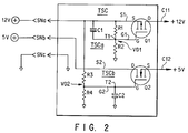
- Fig. 2 TSCa
- TSCb transient suppression circuits
- the first, TSCa is used when there is no voltage supply available which is greater than the voltage being turned on (e.g., a single supply or the highest voltage supply, here, 12v).
- the second, TSCb is used when there is a higher voltage available in the power supply than the voltage being turned on (e.g., turning on 5v when 12v is available).
- the first form of transient suppression circuit, TSCa uses a P channel MOSFET power transistor, Q1 such as seen in Fig. 8 of "Technical Information, Increasing Reliability of SMD Tantalum Capacitors In Low Impedance Applications", pgs. 005 to 015, by David Mattingly, and as seen in "Limiting Voltage And Current Transients On PCB Power Inputs, pgs. 002 to 005, by Matthew Knight.
- This power transistor comprises a source electrode, S, a drain electrode, D, and a gate electrode, G.
- the output circuit of the transient suppression circuit is C11.
- the source electrode circuit, S1 comprises the input circuit.
- the gate electrode circuit, G1 is coupled to and controlled by an intermediate tap, T1, on a resistor type of voltage divider circuit, VD1, the tap voltage of which, in turn, is controlled by a capacitor, C1.
- the voltage divider circuit comprises the resistors, R1 and R2, which are connected in series between the source electrode circuit, S1, and ground.
- the capacitor, C1 is connected between the source electrode circuit, S1, and the intermediate tap, T1, on the voltage divider circuit, VD1.
- the tap, T1 is at 12v.
- This tap voltage which is coupled directly to the gate, G, gates the power transistor, Q1, off.
- the voltage at the tap, T1, is now a function of the ratio of the ohmic values of the resistors, R1 and R2, which gates the power transistor Q1 for full conduction.
- the second form of transient suppression circuit, TSCb employs the voltages of both power circuits, 12v and 5v, to couple power into the 5v output circuit, C12.
- This transient suppression circuit, TSCb comprises an N channel MOSFET power transistor, Q2, a voltage divider circuit, VD2, and a capacitor, C2.
- the source electrode, S is connected in the electrode output circuit, C12.
- the drain electrode, D is connected in the input circuit, S2, which is coupled by the connector, SNb, to the 5v power circuit, and the gate electrode, G, is connected to the tap, T2, of the voltage divider, VD2, by the gate circuit, G2.
- the voltage divider circuit, VD2 comprises resistors, R3 and R4, connected in series between 12v and ground.
- the capacitor, C2 is connected between the tap, T2, (the gate circuit, G2,) and ground.
- the capacitor, C2 holds the gate circuit, G2 at ground potential. This prevents the power transistor, Q2, from conducting.
- the current flow at the capacitor, C2, is controlled by the resistor, R3.
- the rising voltage at the tap, T2, of the voltage divider circuit, VD2 raises the gate voltage of the power transistor, Q2, and conduction increases correspondingly.
- the voltage at the tap, T2 reaches its highest value, set by the resistors, R3 and R4, and the power transistor, Q2, is fully conducting.
- transient suppression system has been described herein making reference to disks as an example of devices being connected to the power supply, other devices may be similarly connected as required. Further, differently configured RAID systems may also be equipped with transient suppression circuits embodying the principles of the types disclosed herein.
Abstract
Description
- This invention relates generally to systems comprising pluralities of devices which are connected to an electrical power supply, in which provision is made for reducing power transients which occur at the time of the connection of a device to the electrical power supply when the system is in operation. In particular, this invention relates to systems embodying redundant arrays of independent devices (RAID), in which, to maintain data and/or reliability, a device, such as a disk drive, is required to be connected to the electrical power supply and integrated into the system while the system is in operation.
- The need for cost effective improvement of mass storage capacity in disk drives has led to the development of redundant arrays of independent devices, such as disk drives, herein referred to as "disks". While disks are usually referred to in describing this invention, it is to be understood that such reference is only for convenience of disclosure and is intended to characterize other devices. The disks are electrically coupled in various arrays and are powered by a common electrical power supply. In these arrays, a typical disk subsystem comprises one or more disk controllers for accessing and controlling the function of individual disks, the functional relationships among the disks and the combinations of disk outputs, to present an appearance, in one RAID mode of operation, of an output from a single disk. Requests to read data from the disks or to write data to the disks are made by a host computer via the disk controllers which establish and maintain the communication link for each request. In this regard, array management software may execute in the disk subsystem (e.g., the disk controllers), or in the host computer, in orchestrating the RAID function.
- The disks are electrically powered by an electrical power supply. When a disk is in operation in the system, the power demand for the disk spindle motor, the rotary actuator motor, magnetic head amplifiers, filter capacitors and other miscellaneous disk circuits is substantially constant and there are no significant power transients. The primary causes of power transients, however, at the time of connection of the disk to the power supply are the filter capacitors of the disk drive. At the time of connection the capacitors are not charged. Since the capacitors are not charged they present a short circuit to the power supply at the time of connection. This is the primary cause of a significant power transient in the electrical power supply. Other types of devices may present similar power transient problems.
- The disks are connected in parallel to the electrical power supply which also supplies power to all electrical components and circuits in the network, including those involved in critical management and logic functions. Power transients in the system, such as momentary power drops, may also disturb the disk speed or disrupt logic circuits sufficiently to disrupt critical RAID system functions, which is unacceptable. Maintenance of, or enlargement of, RAID system data capacity and reliability requires the connection of disks to the system from time-to-time while the system is in operation. Such a connection of a disk, or other device, to the RAID system, whether accomplished manually or automatically, is known as a "hot swap" or "hot plugging".
- The suppression of power transients incident with the connection of a disk to the power supply in a RAID system has received continuing attention. One approach, involving the manual connection of a disk to the power supply of a RAID system, employs an electrical plug connector. The connector has extended length precharge pins. These "precharge" pins have a small resistor connected thereto. When connection is made, this resistor is coupled in series with the power supply. The function of the resistor is to limit current and to precharge capacitors on the device so that when the connection is made to the power bus with the shorter pins there is a smaller difference in voltage and, hence, a smaller transient.
- There are a number of problems with this approach. First, the resistor often has only an intermittent use power rating, e.g., does not have a power rating sufficient to handle the full device current for a long period of time. Therefore, if the connector plug is not fully inserted into the connector receptacle, so that the short pins are quickly engaged, there is a risk of destroying the resistor. The use of a resistor rated for continuous duty to handle the current load, would mean very large and costly parts. The second problem is mostly a cost issue as connectors with multiple pin lengths are more expensive than connectors with only pins of one length. The third problem is that this method of transient suppression is very dependent upon device characteristics as well as timing involved with the insertion of the device, such as a disk.
- There exists a need for a transient suppression system and method which are independent of device characteristics and in which timing is automatic.
- A RAID system of independent devices, such as disks, is functionally arranged and controlled, according to one mode of operation, to present an image to an operating environment, such as a host computer, as though the array were a single disk. In another mode of operation, the array may appear as multiple disks of a predetermined arrangement. The individual disks are powered by an electrical power supply to which the disks are connected. Switches and/or plug connectors are employed to connect the disks to the electrical power supply. The switches may be mechanical, electromechanical or solid state electrical types of switches.
- When the system is in operation, there is need, from time-to-time, to replace or to add a disk to the RAID system. To minimize power transients in the power supply, incident with such connections, a transient suppression circuit is provided, either at the location in the RAID assembly where the connection is to be made, or, as part of the power input circuit to the disk where it is a part of the disk electrical system. At the time, or shortly after the time, that the disk is connected to the power supply, this transient suppression circuit begins to conduct, and, after a short interval of time, controlled by the transient suppression circuit, is fully conducting. This interval of increasing conduction isolates the impedance characteristic of the load from the power supply and thereby controls the power transient.
- The transient suppression circuit comprises an active circuit element. The output circuit of this active circuit element is coupled as input to the disk. The disk is not operating at the time that it is connected to the power supply. The active circuit element is the variable conductor which isolates the load and prevents a power transient at the instant of connection. The active circuit element is preferably a MOSFET power transistor controlled by a capacitor controlled voltage divider circuit which, upon connection to the power supply voltage, initiates and provides the timing function of the transient suppression circuit.
- This invention will be better understood by reference to the following specification when considered in conjunction with the accompanying drawings, in which:
- Fig. 1 is a block diagram of a RAID system embodying a transient suppression circuit, and
- Fig. 2 illustrates transient suppression circuit implementations embodied in the presently known best mode for practicing this invention.
- Fig. 1 illustrates one type of several types of RAID systems and serves to illustrate the principles of this invention. One type of RAID system comprises a plurality of devices, D1, D2, D3, such as disks, which are interconnected and controlled in communication with a host computer, HC, via one or more disk controllers, DC, which manage the disk array. A RAID system, such as this, may function in one mode to present the appearance of a single disk to the host computer. Requests by the host computer HC to read or to write data are translated by the disk controller(s) to head(s), track(s) and track sector(s) (not shown) at the disks where data may be read or written. Reading or writing at the disks may take place on one or more disks in the array, depending upon array management. Raid systems being well known and their array management function not being essential to an understanding of this invention, further description of the Raid function is believed to be unnecessary.
- Fig. 1 illustrates three different ways in which the transient suppression circuit may be functionally integrated with a device. Each disk, D1, D2, D3, is in a device circuit, DC1, DC2, DC3, connected to an electrical power supply, PS. Each device circuit includes a transient suppression circuit, TSC1, TSC2, TSC3, respectively. The power supply, PS, comprises two power circuits of different voltages, 12v and 5v, respectively, and a common circuit, G, usually at ground potential. Electrical connections in the form of connectors, PC1, PC2, PC3, and switches, S2, S3, are provided in the device circuits. The connectors may be of the plug connector type.
- There being three circuits in the power supply, each connector, PC1, PC2, PC3, has three poles, in the form of connector pins CPa, CPb, CPc. As will be seen from Fig. 2, only one switch power pole S2a, S3a, is needed to connect the 12v power supply circuit to the respective transient suppression circuits TSC2, TSC3. Electromagnetically operated switches are shown to simplify conception. Solid state switching is preferably employed in the array environment.
- The first device circuit, DC1, in the RAID system integrates the transient suppression circuit TSC1 electrically and physically with the device, D1. With this arrangement, the connector is employed to manually connect the device, D1, to the power supply, PS. Thus, the transient suppression circuit function is initiated immediately when the connector parts, P1, P2, are joined.
- When the device is to be installed as a spare, for anticipated future use, for example, circuits such as device circuits, DC2, DC3, are useful in making a device installation in preparation for future use.
- In device circuit DC2, the switch, S2, connects the transient suppression circuit, TSC2, to the 12v power supply. This switch is normally open, as shown, and there is no 12v power connection to the transient suppression circuit, TSC2. The device, D2, is connected to the transient suppression circuit by the plug connector, PC2. This circuit provides a basis for the automatic connection of the device, D2, into the RAID system by energizing the electromagnetic actuator, E, closing the switch, S2, and coupling the 12v power supply to the transient suppression circuit, TSC2, initiating the transient suppression function in preparation for connection of the device, D2, to the power supply, PS.
- The device circuit, DC3, is functionally similar to the device circuit, DC2. It differs in the location of the plug connector, PC3. As in the device circuit, DC1, the device, D3, the transient suppression circuit, TSC3, and the plug connector part, P1, of the plug connector, PC3, are electrically and mechanically integrated.
- Other arrangements of the device circuits will be apparent to those skilled in the art.
- In the event that a RAID system requires only a single voltage, such as the voltage 12v, the connectors and the switches, each require only one power pole.
- Upon the application of power, the transient suppression circuits, TSC, function as time varying conductors in which conduction builds up slowly. This function effectively isolates the load impedance of the device from the power supply. Thus, assuming the devices, D1, D2, D3 are disks, when the RAID system is in operation with disks, D1 and D2, operating, if there is a need to connect the disk, D3, to the RAID system, the switch, S3, is closed. The full power of the power supply circuit is coupled to the input of the transient suppression circuit but the rate of change of power across the circuit is slow enough to avoid an unacceptable power transient in the system. The rate at which power increases in the load circuit of the device, D3, is controlled entirely by the transient suppression circuit, not by the load connected to it.
- As detailed in Fig. 2, a transient suppression circuit according to the best known mode for practicing this invention, comprises an active circuit which is controlled by a capacitor controlled voltage divider circuit responsive to the voltage of the power supply, whether the power supply has one or two different voltages.
- In the best known mode for practicing this invention, the active circuit of the transient suppression circuit, for either the 12v or the 12v, 5v power supply, comprises a MOSFET power transistor, Q1, or Q2, respectively as the time varying conductor. This is seen in Fig. 2. When the transient suppression circuit, TSCa or TSCb, is first connected to the power supply, PS, the power transistor, Q1 or Q2, is off. After the power connection, the conduction of the power transistor, Q1 or Q2, increases as a function of time, time varying conduction, controlled by the capacitor, C1 or C2, slowly increasing the voltage coupled to the disk. When the power transistor is fully conducting, the power supply "sees" the load impedance of the disk which is now powered directly from the power supply. Full conduction timing of the power transistor is timed to permit the load impedance to have stabilized.
- There are two forms of transient suppression circuits, TSC, illustrated in Fig. 2, TSCa, TSCb. The first, TSCa, is used when there is no voltage supply available which is greater than the voltage being turned on (e.g., a single supply or the highest voltage supply, here, 12v). The second, TSCb, is used when there is a higher voltage available in the power supply than the voltage being turned on (e.g., turning on 5v when 12v is available).
- The first form of transient suppression circuit, TSCa, uses a P channel MOSFET power transistor, Q1 such as seen in Fig. 8 of "Technical Information, Increasing Reliability of SMD Tantalum Capacitors In Low Impedance Applications", pgs. 005 to 015, by David Mattingly, and as seen in "Limiting Voltage And Current Transients On PCB Power Inputs, pgs. 002 to 005, by Matthew Knight. This power transistor comprises a source electrode, S, a drain electrode, D, and a gate electrode, G. The output circuit of the transient suppression circuit is C11. The source electrode circuit, S1, comprises the input circuit. The gate electrode circuit, G1, is coupled to and controlled by an intermediate tap, T1, on a resistor type of voltage divider circuit, VD1, the tap voltage of which, in turn, is controlled by a capacitor, C1. The voltage divider circuit comprises the resistors, R1 and R2, which are connected in series between the source electrode circuit, S1, and ground. The capacitor, C1, is connected between the source electrode circuit, S1, and the intermediate tap, T1, on the voltage divider circuit, VD1.
- At the time when the power supply circuit, 12v, is connected to the transient suppression circuit, TSCa, the tap, T1, is at 12v. This tap voltage which is coupled directly to the gate, G, gates the power transistor, Q1, off. The tap voltage at the tap, T1, as controlled by the capacitor, decreases and the power transistor, Q1, begins to conduct, being turned on fully when the current flow at the capacitor, C1, ceases. The voltage at the tap, T1, is now a function of the ratio of the ohmic values of the resistors, R1 and R2, which gates the power transistor Q1 for full conduction.
- The second form of transient suppression circuit, TSCb, employs the voltages of both power circuits, 12v and 5v, to couple power into the 5v output circuit, C12. This transient suppression circuit, TSCb, comprises an N channel MOSFET power transistor, Q2, a voltage divider circuit, VD2, and a capacitor, C2. The source electrode, S, is connected in the electrode output circuit, C12. The drain electrode, D, is connected in the input circuit, S2, which is coupled by the connector, SNb, to the 5v power circuit, and the gate electrode, G, is connected to the tap, T2, of the voltage divider, VD2, by the gate circuit, G2. The voltage divider circuit, VD2, comprises resistors, R3 and R4, connected in series between 12v and ground. The capacitor, C2, is connected between the tap, T2, (the gate circuit, G2,) and ground.
- At the instant that the switch, SN, is closed, the capacitor, C2, holds the gate circuit, G2 at ground potential. This prevents the power transistor, Q2, from conducting. The current flow at the capacitor, C2, is controlled by the resistor, R3. The rising voltage at the tap, T2, of the voltage divider circuit, VD2, raises the gate voltage of the power transistor, Q2, and conduction increases correspondingly. When current flow at the capacitor C2 ceases, the voltage at the tap, T2, reaches its highest value, set by the resistors, R3 and R4, and the power transistor, Q2, is fully conducting.
- The advantages of these transient suppression circuits are that the turn on time is automatically controlled by the values of the resistors and the capacitors in the control circuits; there is no passive current limiting element in the power circuits, so the problem of power dissipation in such an element is eliminated; the load being coupled to the power supply is isolated from the power supply, and, since the timing function is automatic, there is no need for connectors with pins of different lengths.
- While the transient suppression system has been described herein making reference to disks as an example of devices being connected to the power supply, other devices may be similarly connected as required. Further, differently configured RAID systems may also be equipped with transient suppression circuits embodying the principles of the types disclosed herein.
Claims (9)
- A system of control for electrically interconnected discrete devices. comprising:a. an electrical power supply (PS);b. a plurality of discrete devices (D1, D2, D3) connected to said electrical power supply (5v, 12v);c. a control circuit (DC1, DC2, DC3) for electrically interconnecting and controlling said discrete devices in a predetermined functional relationship;d. a transient suppression circuit (TSC1, or TSC2, or TSC3) for at least one discrete device (D1, or D2, or D3), said transient suppression circuit (TSC1, or TSC2, or TSC3) comprising an active circuit element (Q1 or Q2), said active circuit element (Q1 or Q2) having an output circuit (C11 or C12) connected to said at least one discrete device (Q1 or Q2) and having an input circuit (S1 or S2);e. said transient suppression circuit (TSC1, or TSC2, or TSC3) further comprising a capacitor controlled voltage divider circuit (VD1 or VD2) for coupling a time varying voltage to said active circuit element ((Q1 or Q2) to control conduction of said active circuit element (q1 or Q2), andf. connector means (S2 or S3) for coupling said power supply circuit (PS) to said input circuit (S1 or S2) and to said capacitor controlled voltage divider circuit (VD1 or VD2).
- The system according to claim 1, in which:a. said active output circuit element (Q1 or Q2) comprises a power transistor.
- The system according to claim 2, in which:a. said power transistor (Q1 or Q2) comprises a MOSFET power transistor.
- The system according to claim 1, in which:a. said active circuit element (Q1 or Q2) is a power transistor having a source (S), a drain (D) and a gate (G), said drain (D) being connected in said output circuit (C11), said source (S) being connected to said power supply (PS) by said connector means (S2 or S3);b. said voltage divider circuit (VD1 or VD2) comprises at least two series connected resistors (R1, R2, or R3, R4) having an intermediate tap (T1 or T2) connected to said gate (G), said connector means (S2 or S3) connecting said voltage divider circuit (VD1 or VD2) to said power supply (PS), andc. said capacitor (C1 or C2) being connected to said intermediate tap (T1 or T2) and having a charging rate controlled by one resistor (R2 or R3) of said voltage divider circuit (VD1 or VD2).
- The system according to claim 1, in which;a. Said power supply circuit (PS) comprises at least one voltage circuit (V);b. said active circuit element (Q1 or Q2) is a power transistor having a source (S), a drain (D) and a gate (G), said drain (D) being connected in said output circuit (C11), said source (S) being connected to said at least one voltage circuit (12v) of said power supply circuit (PS) by said connector means (S2 or S3);c. said voltage divider circuit (VD1 or VD2) comprises at least two series connected resistors (R1, R2 or R3, R4) having an intermediate tap (T1 or T2) connected to said gate (G);d. said capacitor (C1 or C2) is connected to said intermediate tap (T1 or T2) of said voltage divider circuit (VD1 or VD2), ande. said voltage divider circuit (VD1 or VD2) and said capacitor (C1 or C2) are connected to said power supply (PS) by said connector means (S2 or S3).
- The system according to claim 1, in which:a. said electrical power supply circuit (PS) comprises a first voltage circuit of a first voltage (12v) and a second voltage circuit of a second voltage (5v);b. said active circuit element (Q2) is a power transistor having a source (S), a drain (D) and a gate (G) said source (S) and said drain (D) connected between said output circuit (C12) and said second voltage circuit (5v) of said power supply (PS);c. said voltage divider circuit (VD2) comprises at least two series connected resistors (R3, R4) having a tap (T2) connected to said gate (G) said voltage divider (circuit T2) connected to said first voltage circuit (12v) of said power supply (PS) by said connector means (SNa), said capacitor (C2) connected between said tap (T2) of said voltage divider circuit (VD2) and ground.
- A system of electrically interconnected discrete devices having provision for connecting a discrete device while the system is in operation, comprising:a. an electrical power supply (PS);b. a plurality of discrete devices (D1, D2 or D3) connected to said electrical power supply (PS);c. a device controller (DC) for electrically interconnecting and controlling said discrete devices (D1, D2, or D3) in a predetermined functional relationship;d. a single discrete device to be coupled to said power supply;e. an active circuit element (Q1) for coupling electrical power from said power supply (PS, 12v) to said single discrete device (Q1);f. a control circuit (VD1) for producing a time varying control signal for a predetermined interval of time, initiated when electrical power (PS, 12v) is coupled to said control circuit (VD1), for initiating time varying conduction of said active circuit element (Q1) within said predetermined interval of time, andg. an electrical connector (SNa) for coupling said active circuit element (Q1) and said control circuit (VD1) to said electrical power supply (PS).
- The system according to claim 7, in which:a. said active circuit element (Q1) is a MOSFET power transistor.
- The system according to claim 7, in which:a. said active circuit element (Q1) is a MOSFET power transistor, andb. said control circuit (VD1) is a capacitor (C1) controlled voltage divider circuit (R1, R2).
Applications Claiming Priority (2)
| Application Number | Priority Date | Filing Date | Title |
|---|---|---|---|
| US33146894A | 1994-10-31 | 1994-10-31 | |
| US331468 | 1994-10-31 |
Publications (3)
| Publication Number | Publication Date |
|---|---|
| EP0709962A2 true EP0709962A2 (en) | 1996-05-01 |
| EP0709962A3 EP0709962A3 (en) | 1997-02-26 |
| EP0709962B1 EP0709962B1 (en) | 2002-10-02 |
Family
ID=23294109
Family Applications (1)
| Application Number | Title | Priority Date | Filing Date |
|---|---|---|---|
| EP19950110831 Expired - Lifetime EP0709962B1 (en) | 1994-10-31 | 1995-07-11 | System for suppressing power transients when connecting a disk drive in an operating RAID system |
Country Status (4)
| Country | Link |
|---|---|
| US (1) | US5587685A (en) |
| EP (1) | EP0709962B1 (en) |
| JP (1) | JPH08211969A (en) |
| DE (1) | DE69528431T2 (en) |
Cited By (3)
| Publication number | Priority date | Publication date | Assignee | Title |
|---|---|---|---|---|
| DE20315837U1 (en) * | 2003-10-15 | 2005-03-03 | Weidmüller Interface GmbH & Co. KG | Distributor for connecting electrical equipment with multiple power supply |
| WO2020094459A1 (en) * | 2018-11-06 | 2020-05-14 | HELLA GmbH & Co. KGaA | Circuit arrangement for limiting an inrush current |
| US11955478B2 (en) | 2019-05-07 | 2024-04-09 | Cambridge Gan Devices Limited | Power semiconductor device with an auxiliary gate structure |
Families Citing this family (27)
| Publication number | Priority date | Publication date | Assignee | Title |
|---|---|---|---|---|
| JP2682503B2 (en) * | 1995-03-24 | 1997-11-26 | 日本電気株式会社 | Hot-swap system |
| US5774315A (en) * | 1996-08-19 | 1998-06-30 | Core Engineering, Inc. | Power surge suppression circuit for hot plug environments |
| US5864457A (en) * | 1997-01-21 | 1999-01-26 | Dell Usa, L.P. | System and method for controlling current flow in an AC adapter |
| KR100256609B1 (en) * | 1997-06-03 | 2000-05-15 | 윤종용 | Overvoltage and surge protection circuit in a hard disk drive |
| US5990723A (en) * | 1998-01-09 | 1999-11-23 | Maxim Integrated Products, Inc. | Filter circuits for protecting against transient electrical pulses |
| US6098119A (en) * | 1998-01-21 | 2000-08-01 | Mylex Corporation | Apparatus and method that automatically scans for and configures previously non-configured disk drives in accordance with a particular raid level based on the needed raid level |
| JP4412685B2 (en) * | 1998-09-28 | 2010-02-10 | 株式会社日立製作所 | Storage controller and method of handling data storage system using the same |
| US6473283B1 (en) | 2000-01-12 | 2002-10-29 | Mp Electronics, Inc. | Voltage protection circuit for multi-drop bus of an automated coin vending machine |
| US20020071231A1 (en) * | 2000-12-12 | 2002-06-13 | Chloupek James E | Hard disk drive (HDD) electrical over voltage stress (EOS) systems and methods |
| WO2002067279A2 (en) * | 2000-12-22 | 2002-08-29 | Ixys Corporation | Hot-swap protection circuit |
| KR100828923B1 (en) * | 2001-10-10 | 2008-05-13 | 엘지디스플레이 주식회사 | Prevention Circuit of Over Voltage and Surge Voltage |
| TW511271B (en) * | 2001-10-19 | 2002-11-21 | Winbond Electronics Corp | Electrostatic discharge protection circuit with high electrostatic discharge tolerance capability |
| US6703889B2 (en) | 2002-02-14 | 2004-03-09 | Adc Dsl Systems, Inc. | In-rush current protection |
| US20030206386A1 (en) * | 2002-05-01 | 2003-11-06 | Hill Christopher Lawrence | Power supply isolation during motor spinup |
| US6807039B2 (en) * | 2002-07-08 | 2004-10-19 | Adc Dsl Systems, Inc. | Inrush limiter circuit |
| US20040070908A1 (en) * | 2002-09-27 | 2004-04-15 | International Business Machines Corporation | Overcurrent protection of input/output devices in a data processing system |
| TWI243230B (en) * | 2004-07-16 | 2005-11-11 | Delta Electronics Inc | Hot-swap circuit system for fan tray |
| US7573156B2 (en) * | 2005-12-22 | 2009-08-11 | American Power Conversion Corporation | Apparatus for and method of connecting a power source to a device |
| US7849261B2 (en) * | 2006-06-29 | 2010-12-07 | Seagate Technology Llc | Temperature control to reduce cascade failures in a multi-device array |
| US7661005B2 (en) * | 2006-06-30 | 2010-02-09 | Seagate Technology Llc | Individual storage device power control in a multi-device array |
| US7495878B2 (en) * | 2007-03-22 | 2009-02-24 | Bae Systems Information And Electronic Systems Integration Inc. | Decoupling capacitor control circuit and method for enhanced ESD performance |
| US8503201B2 (en) | 2009-12-03 | 2013-08-06 | Schneider Electric It Corporation | Transient clamping circuitry for voltage converter |
| CN102270839B (en) * | 2010-06-07 | 2014-06-18 | 飞利浦建兴数位科技股份有限公司 | Electronic device with protective circuit |
| US8498088B1 (en) | 2011-12-21 | 2013-07-30 | Western Digital Technologies, Inc. | Storage device with replaceable protection device |
| US9112345B2 (en) | 2012-06-06 | 2015-08-18 | Honeywell International Inc. | In-rush current limiter and method for stowable and carry-on devices |
| WO2014032302A1 (en) | 2012-09-03 | 2014-03-06 | Schneider Electric It Corporation | Method and apparatus for controlling distribution of power |
| GB2564482B (en) * | 2017-07-14 | 2021-02-10 | Cambridge Entpr Ltd | A power semiconductor device with a double gate structure |
Citations (7)
| Publication number | Priority date | Publication date | Assignee | Title |
|---|---|---|---|---|
| EP0272514A1 (en) * | 1986-12-23 | 1988-06-29 | Siemens Aktiengesellschaft | Circuit arrangement for limiting the switch-on current and for overvoltage protection of switched power supply apparatuses |
| DE3804250C1 (en) * | 1988-02-11 | 1989-07-27 | Siemens Ag, 1000 Berlin Und 8000 Muenchen, De | Circuit arrangement for a current limiter |
| EP0356186A2 (en) * | 1988-08-24 | 1990-02-28 | Stc Plc | Power control circuit for electronic equipment |
| EP0369180A2 (en) * | 1988-11-07 | 1990-05-23 | STMicroelectronics S.r.l. | A circuit device, made up of a reduced number of components, for simultaneously turning on a plurality of power transistors |
| EP0490010A1 (en) * | 1990-12-07 | 1992-06-17 | International Business Machines Corporation | Hot-plugging circuit for the interconnection of cards to boards |
| EP0551718A2 (en) * | 1991-11-25 | 1993-07-21 | Tandem Computers Incorporated | System and method for ensuring write data integrity in a redundant array data storage system |
| DE4330996A1 (en) * | 1993-09-13 | 1995-03-16 | Bosch Gmbh Robert | Control device for an electric load, particularly an inductive load |
Family Cites Families (8)
| Publication number | Priority date | Publication date | Assignee | Title |
|---|---|---|---|---|
| US4233566A (en) * | 1978-10-23 | 1980-11-11 | Technical Audio Products Corporation | Distortion free power limiting and clipping prevention circuit |
| US4245270A (en) * | 1978-12-26 | 1981-01-13 | Rockwell International Corporation | Circuit card with soft power switch |
| US4329705A (en) * | 1979-05-21 | 1982-05-11 | Exxon Research & Engineering Co. | VMOS/Bipolar power switching device |
| US4620272A (en) * | 1984-08-31 | 1986-10-28 | Imec Corporation | Line-regenerative motor controller with current limiter |
| US5268592A (en) * | 1991-02-26 | 1993-12-07 | International Business Machines Corporation | Sequential connector |
| US5313358A (en) * | 1991-12-13 | 1994-05-17 | Premier Power, Inc. | Multiphase common mode transient suppressor |
| US5283707A (en) * | 1992-11-27 | 1994-02-01 | Northern Telecom Limited | Inrush current limiting circuit |
| JP2738801B2 (en) * | 1993-01-26 | 1998-04-08 | 三菱電機株式会社 | Hot-swap circuit |
-
1995
- 1995-07-11 DE DE1995628431 patent/DE69528431T2/en not_active Expired - Lifetime
- 1995-07-11 EP EP19950110831 patent/EP0709962B1/en not_active Expired - Lifetime
- 1995-10-30 JP JP30505895A patent/JPH08211969A/en active Pending
- 1995-11-22 US US08/562,263 patent/US5587685A/en not_active Expired - Lifetime
Patent Citations (7)
| Publication number | Priority date | Publication date | Assignee | Title |
|---|---|---|---|---|
| EP0272514A1 (en) * | 1986-12-23 | 1988-06-29 | Siemens Aktiengesellschaft | Circuit arrangement for limiting the switch-on current and for overvoltage protection of switched power supply apparatuses |
| DE3804250C1 (en) * | 1988-02-11 | 1989-07-27 | Siemens Ag, 1000 Berlin Und 8000 Muenchen, De | Circuit arrangement for a current limiter |
| EP0356186A2 (en) * | 1988-08-24 | 1990-02-28 | Stc Plc | Power control circuit for electronic equipment |
| EP0369180A2 (en) * | 1988-11-07 | 1990-05-23 | STMicroelectronics S.r.l. | A circuit device, made up of a reduced number of components, for simultaneously turning on a plurality of power transistors |
| EP0490010A1 (en) * | 1990-12-07 | 1992-06-17 | International Business Machines Corporation | Hot-plugging circuit for the interconnection of cards to boards |
| EP0551718A2 (en) * | 1991-11-25 | 1993-07-21 | Tandem Computers Incorporated | System and method for ensuring write data integrity in a redundant array data storage system |
| DE4330996A1 (en) * | 1993-09-13 | 1995-03-16 | Bosch Gmbh Robert | Control device for an electric load, particularly an inductive load |
Non-Patent Citations (1)
| Title |
|---|
| ELEKTOR ELECTRONICS, vol. 21, no. 235, 1 July 1995, page 100 XP000515472 ZEILLER W: "SOFT START SWITCH FOR DC MOTORS" * |
Cited By (4)
| Publication number | Priority date | Publication date | Assignee | Title |
|---|---|---|---|---|
| DE20315837U1 (en) * | 2003-10-15 | 2005-03-03 | Weidmüller Interface GmbH & Co. KG | Distributor for connecting electrical equipment with multiple power supply |
| US7230820B2 (en) | 2003-10-15 | 2007-06-12 | Weidmüller Interface GmbH & Co.KG | Distributor means for connecting electrical apparatus with a plurality of voltage sources |
| WO2020094459A1 (en) * | 2018-11-06 | 2020-05-14 | HELLA GmbH & Co. KGaA | Circuit arrangement for limiting an inrush current |
| US11955478B2 (en) | 2019-05-07 | 2024-04-09 | Cambridge Gan Devices Limited | Power semiconductor device with an auxiliary gate structure |
Also Published As
| Publication number | Publication date |
|---|---|
| DE69528431D1 (en) | 2002-11-07 |
| EP0709962A3 (en) | 1997-02-26 |
| EP0709962B1 (en) | 2002-10-02 |
| DE69528431T2 (en) | 2003-07-03 |
| JPH08211969A (en) | 1996-08-20 |
| US5587685A (en) | 1996-12-24 |
Similar Documents
| Publication | Publication Date | Title |
|---|---|---|
| US5587685A (en) | System for suppressing power transients when connecting a disk drive in an operating raid system | |
| US5272584A (en) | Hot-plugging circuit for the interconnection of cards to boards | |
| US6026458A (en) | System with pluggable adapter card and hot-swap interface controller | |
| US5432916A (en) | Precharge for non-disruptive bus live insertion | |
| US5210855A (en) | System for computer peripheral bus for allowing hot extraction on insertion without disrupting adjacent devices | |
| US5422580A (en) | Switchable active termination for SCSI peripheral devices | |
| US7671485B2 (en) | Storage system | |
| US5519882A (en) | System for configuring a disk drive as a master or slave by either cable or local selection with only one jumper block or one switching device | |
| US9984762B1 (en) | Cascaded E-fuse switch circuits to control data backup in a storage device | |
| US5898844A (en) | Data processing system including a hot-plug circuit for receiving high-power adaptor cards | |
| US5909065A (en) | Multi-stage precharging system to limit power supply transients when printed circuit boards are plugged in | |
| US20050193159A1 (en) | Embedded power control circuitry for a portable disk drive carrier having a hot-plug application | |
| EP0402055A2 (en) | Method and apparatus for a rapid interconnection to a computer bus | |
| US6289407B1 (en) | Input/output device for connection and disconnection of active lines | |
| JPH0845266A (en) | Module card | |
| US6038615A (en) | Input/output device for connection and disconnection of active lines | |
| US20020133660A1 (en) | Input/output device for connection and disconnection of active lines | |
| US20040057182A1 (en) | Method and control apparatus for controlling two hot-swapable IDE devices | |
| CN1221078C (en) | Surge current preventing and time sequence controlling device and method for thermal connect-disceonnect electronic equipment | |
| US20050157479A1 (en) | Bus device insertion and removal system | |
| US6415346B1 (en) | Pre-charging logic cards for hot insertion | |
| US20040012263A1 (en) | Method and apparatus for integrated circuit power up | |
| JP3997107B2 (en) | Hot-line insertion / removal device and hot-line insertion / extraction method | |
| CN100353551C (en) | Semiconductor integrated circuit device | |
| KR20000064640A (en) | Bus segment or bus interface for connecting a subassembly of programmable controllers to the bus |
Legal Events
| Date | Code | Title | Description |
|---|---|---|---|
| PUAI | Public reference made under article 153(3) epc to a published international application that has entered the european phase |
Free format text: ORIGINAL CODE: 0009012 |
|
| AK | Designated contracting states |
Kind code of ref document: A2 Designated state(s): DE FR GB |
|
| PUAL | Search report despatched |
Free format text: ORIGINAL CODE: 0009013 |
|
| AK | Designated contracting states |
Kind code of ref document: A3 Designated state(s): DE FR GB |
|
| RTI1 | Title (correction) | ||
| 17P | Request for examination filed |
Effective date: 19970414 |
|
| RAP1 | Party data changed (applicant data changed or rights of an application transferred) |
Owner name: HEWLETT-PACKARD COMPANY, A DELAWARE CORPORATION |
|
| 17Q | First examination report despatched |
Effective date: 20010529 |
|
| GRAG | Despatch of communication of intention to grant |
Free format text: ORIGINAL CODE: EPIDOS AGRA |
|
| GRAG | Despatch of communication of intention to grant |
Free format text: ORIGINAL CODE: EPIDOS AGRA |
|
| GRAH | Despatch of communication of intention to grant a patent |
Free format text: ORIGINAL CODE: EPIDOS IGRA |
|
| GRAH | Despatch of communication of intention to grant a patent |
Free format text: ORIGINAL CODE: EPIDOS IGRA |
|
| GRAA | (expected) grant |
Free format text: ORIGINAL CODE: 0009210 |
|
| AK | Designated contracting states |
Kind code of ref document: B1 Designated state(s): DE FR GB |
|
| REG | Reference to a national code |
Ref country code: GB Ref legal event code: FG4D |
|
| REF | Corresponds to: |
Ref document number: 69528431 Country of ref document: DE Date of ref document: 20021107 |
|
| ET | Fr: translation filed | ||
| PLBE | No opposition filed within time limit |
Free format text: ORIGINAL CODE: 0009261 |
|
| STAA | Information on the status of an ep patent application or granted ep patent |
Free format text: STATUS: NO OPPOSITION FILED WITHIN TIME LIMIT |
|
| 26N | No opposition filed |
Effective date: 20030703 |
|
| PGFP | Annual fee paid to national office [announced via postgrant information from national office to epo] |
Ref country code: GB Payment date: 20050706 Year of fee payment: 11 |
|
| PGFP | Annual fee paid to national office [announced via postgrant information from national office to epo] |
Ref country code: FR Payment date: 20050718 Year of fee payment: 11 |
|
| PG25 | Lapsed in a contracting state [announced via postgrant information from national office to epo] |
Ref country code: GB Free format text: LAPSE BECAUSE OF NON-PAYMENT OF DUE FEES Effective date: 20060711 |
|
| GBPC | Gb: european patent ceased through non-payment of renewal fee |
Effective date: 20060711 |
|
| REG | Reference to a national code |
Ref country code: FR Ref legal event code: ST Effective date: 20070330 |
|
| PG25 | Lapsed in a contracting state [announced via postgrant information from national office to epo] |
Ref country code: FR Free format text: LAPSE BECAUSE OF NON-PAYMENT OF DUE FEES Effective date: 20060731 |
|
| PGFP | Annual fee paid to national office [announced via postgrant information from national office to epo] |
Ref country code: DE Payment date: 20110727 Year of fee payment: 17 |
|
| PG25 | Lapsed in a contracting state [announced via postgrant information from national office to epo] |
Ref country code: DE Free format text: LAPSE BECAUSE OF NON-PAYMENT OF DUE FEES Effective date: 20130201 |
|
| REG | Reference to a national code |
Ref country code: DE Ref legal event code: R119 Ref document number: 69528431 Country of ref document: DE Effective date: 20130201 |