EP0708451B1 - Semiconductor memory device - Google Patents
Semiconductor memory device Download PDFInfo
- Publication number
- EP0708451B1 EP0708451B1 EP95115639A EP95115639A EP0708451B1 EP 0708451 B1 EP0708451 B1 EP 0708451B1 EP 95115639 A EP95115639 A EP 95115639A EP 95115639 A EP95115639 A EP 95115639A EP 0708451 B1 EP0708451 B1 EP 0708451B1
- Authority
- EP
- European Patent Office
- Prior art keywords
- signal
- block
- blocks
- inverters
- mosfet
- Prior art date
- Legal status (The legal status is an assumption and is not a legal conclusion. Google has not performed a legal analysis and makes no representation as to the accuracy of the status listed.)
- Expired - Lifetime
Links
Images


Classifications
-
- G—PHYSICS
- G11—INFORMATION STORAGE
- G11C—STATIC STORES
- G11C29/00—Checking stores for correct operation ; Subsequent repair; Testing stores during standby or offline operation
-
- G—PHYSICS
- G11—INFORMATION STORAGE
- G11C—STATIC STORES
- G11C29/00—Checking stores for correct operation ; Subsequent repair; Testing stores during standby or offline operation
- G11C29/04—Detection or location of defective memory elements, e.g. cell constructio details, timing of test signals
- G11C29/50—Marginal testing, e.g. race, voltage or current testing
-
- G—PHYSICS
- G11—INFORMATION STORAGE
- G11C—STATIC STORES
- G11C29/00—Checking stores for correct operation ; Subsequent repair; Testing stores during standby or offline operation
- G11C29/04—Detection or location of defective memory elements, e.g. cell constructio details, timing of test signals
- G11C29/08—Functional testing, e.g. testing during refresh, power-on self testing [POST] or distributed testing
- G11C29/12—Built-in arrangements for testing, e.g. built-in self testing [BIST] or interconnection details
- G11C29/18—Address generation devices; Devices for accessing memories, e.g. details of addressing circuits
- G11C29/24—Accessing extra cells, e.g. dummy cells or redundant cells
-
- G—PHYSICS
- G11—INFORMATION STORAGE
- G11C—STATIC STORES
- G11C16/00—Erasable programmable read-only memories
- G11C16/02—Erasable programmable read-only memories electrically programmable
- G11C16/04—Erasable programmable read-only memories electrically programmable using variable threshold transistors, e.g. FAMOS
Definitions
- This invention relates to a semiconductor memory device and particularly to memory cells of NAND type EEPROMs(Electrically Erasable Programmable Read Only Memory) which are suitable for life tests performed in a test mode.
- NAND type EEPROMs Electrically Erasable Programmable Read Only Memory
- Fig. 1 is a typical cross-sectional view of a memory cell of an EEPROM.
- a source 1 and a drain 2 are Formed on a surface of a silicon substrate 7 a source 1 and a drain 2 at both sides of a channel 5.
- a floating gate 4 Made on the source 1, drain 2 and channel 5 is a floating gate 4 via an oxide film 6.
- a portion of the oxide film 6 lying on the drain 2 is made thinner than other portions so that it behaves as a tunneling oxide film 6a.
- a control gate 3 Further formed on the floating gate 4 is a control gate 3 via another oxide film, and the entirety is covered by a further oxide film.
- Storage of data in the memory cell of the EEPROM is performed by storing binary numbers 0 and 1, depending on the presence or absence of electrons on the floating gate 4. That is, if the potential of the channel 5 between the drain 2 and the source 1 is set to 0V by applying a high voltage to the control gate 3, then a high electric field is produced in the oxide layer 6 between the floating gate 4 and the channel 5, which causes a tunneling current to flow through the tunneling oxide film 6a and causes electrons to be trapped on the floating gate 4. Then the threshold voltage of the memory cell increases (writing). To the contrary, if the potential of the control gate 3 is set to 0V, electrons are pulled out from the floating gate 4 into the channel 5. Thus the threshold voltage of the memory cell decreases (erasure).
- the control of the threshold voltage of the memory cell during writing and erasure relies on the tunneling current in the oxide film in the presence of a high electric field. Since the tunneling current is very small, it can be supplied to a plurality of memory cells simultaneously. Therefore, a NAND type EEPROM can be designed to stand for the mode for simultaneous writing and simultaneous erasure as a test mode such that all memory blocks (hereinafter simply called blocks), each comprising a plurality of memory cells, can be accessed simultaneously for write and erase operations by supplying an external signal.
- the high voltage required for writing and erasure is generated by a booster circuit built in the device. Although the voltage is about 24v in most cases, there are trial devices using higher voltage values.
- NAND type EEPROMs have redundant blocks and switching circuits for replacement of a defective block, if any, by one of the redundant blocks. If a defective block is found by a test in the wafer phase, the defective block is replaced by a redundant block and is held in a non-selected state by blowing (cutting off) the fuse. Then the device is used as a non-defective product.
- Fig. 2 is a circuit diagram of a conventional NAND EEPROM which includes four blocks BLK1 to BLK4 having block addresses BA0, BA1, /BA0, /BA1, respectively, and two redundant blocks SBLK1 and SBLK2 prepared as spare blocks.
- 3-input NAND gates ND41 to ND44 are provided in combination with four blocks BLK1 to BLK4 for normal use, respectively, and 2-input NAND gates ND45, ND46 are provided in combination with two redundant blocks SBLK1 and SBLK2, respectively.
- inverse logic signals are expressed by attaching "/" to original logic signals. In the drawings, however, they are shown by attaching an upper bar according to the usual practice for expressing inverse logic signals.
- Each of the NAND gates ND41 to ND44 associated with blocks BLK1 to BLK4 is supplied with two block address signals designating a respective block and a switch signal for replacing the block with a redundant block.
- Each of the redundant blocks SBLK1 and SBLK2 associated with the NAND gates ND45 and ND46 is supplied with two block address signals designating a respective block.
- fuses f a and f d among fuses f e to f d for SBLK1 1 are blown.
- the externally supplied control signal /CPE Chip Enable
- the signal /CPE* obtained from /CPE through the buffer is the same logic signal as /CPE.
- /CPE* also becomes L.
- RDE Redundancy Enable
- the device can be used as a non-defective product.
- V 10 L
- the device even though the device exhibits a completely non-defective product when used in all modes except for the test mode, once it is put in the test mode for performing a life test by applying a high voltage for simultaneous writing and erasure, the device falls into the status where, due to the presence of the defective blocks, the regular voltage is not applied to the other non-defective blocks, and the test cannot be executed.
- a semiconductor memory is known to perform a stress test for checking memory cells or a burn-in test for checking voltage-withstanding property even if certain bit- or wordlines are defected.
- a normal stress potential is applied to other normal bitlines or bitlines in blocks other than the block containing the defective bitline, thereby permitting a proper check to be made for reliability.
- a burn-in test for checking voltage-withstanding property a normal stress potential is applied to other normal wordlines, thereby permitting a proper burn-in test to be made.
- a redundancy selecting circuit for selecting the redundancy bitlines and a faulty address storing circuit which stores the addresses for substituting redundancy bitlines as well as a controlling circuit which controls the selecting circuit is provided.
- EP 0 600 151 A refers to a non-volatile semiconductor memory device having electrically and collectively erasable characteristics.
- the device has a first unit for simultaneously selecting a block of 2 m wordlines among 2 n wordlines (n > m), and a second unit for not selecting a block of 2 k wordlines among the 2 m (m > k).
- the second unit does not select the block of 2 k wordlines and selects a block of 2 k wordlines prepared outside the 2 n wordlines when any of the 2 k wordlines among the 2 m is defective.
- means for supplying a write drain voltage to a cell transistor independent of the threshold voltage of a write voltage supply transistor is provided to enable correct writing with a low write voltage.
- the device includes block selecting circuits which prohibit application of the voltage for simultaneous writing and erasure to defective blocks when the device is in the mode for access to all blocks for simultaneous writing and erasure. After the defective blocks are replaced with redundant blocks, the high voltage generated by the booster circuit for simultaneous writing and erasure of all blocks is prevented from dropping due to leakage of the current from the defective blocks. Therefore, the device can be used as a non-defective NAND type EEPROM in all modes including the test mode, provided the defective blocks are replaced by redundant blocks.
- each block selecting circuit is configured to output a "NON-SELECT" signal when it receives the signal instructing simultaneous writing and simultaneous erasure after the fuse is blown, the voltage for simultaneous write and erase is never applied to the defective block replaced by a redundant block.
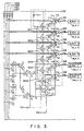
- Figs. 3 is a circuit diagram of a NAND EEPROM having block selecting circuits, taken as an embodiment of the invention.
- This is a circuit in which a respective block selecting circuit is provided in the box drawn with the dotted line in Fig. 3 to make a pair with each block in the circuit of Fig. 2 , shown as prior art, which includes four blocks BLK1-BLK4 having block addresses BA0, BA1, /BA0, /BA1, and two spare redundant blocks SBLK1 and SBLK2.
- Each block selecting circuit is made of an inverter INV1 and corresponding one of circuits BSC1 to BSC6.
- 4-input NAND gates ND1 to ND4 are provided for normally used blocks BLK1 to BLK4, respectively, and 3-input NAND gates ND5 to ND6 are provided for redundant blocks SBLK1 and SBLK2.
- the NAND gates ND1 to ND4 associated with BLK1 to BLK4 are supplied with two block address signals designating individual blocks and a switch signal for switching from the block to a redundant block.
- the NAND gates ND5 and ND6 for the redundant blocks SBLK1 and SBLK2 are supplied with two block address signals designating the respective blocks.
- the NAND gates ND1 to ND6 for BLK1 to BLK4, and for SBLK1 and SBLK2 are supplied with output signals from respective block selecting circuits. The block selecting circuits are explained below in greater detail.
- Fig. 4 is a circuit diagram of an elemental unit of the block selecting circuits according to an embodiment of the invention, Fig. 4 shows one of the BSC circuits coupled to the inverter INV1 in the circuit of Fig. 3.
- the input terminal a is coupled to the common gate input terminal b of a CMOS inverter INV20 via an inverter INV10 on one hand and directly to a gate terminal c of a MOSFET Q10 on the other hand.
- One of the source and drain of the MOSFET Q10 is grounded, and the other of them is coupled to the output point d via a fuse F and further to the output terminal e through an inverter INV30.
- the block selecting circuit operates as follows, where signal voltages at points a, b, c, d and e are labelled V a , V b , V c , V d and V e .
- V d L
- V b H
- V d L
- any appropriate element such as a PROM may be used.
- the MOSFET is any appropriate element capable of supplying "SELECT" signal “H” by changing the signal “H” at point d into “L” when signal "H” is input while the path to point d is held connected.
- a respective block selecting circuit comprising the inverter INV1 and a respective one of the circuits BSC1 to BSC6 is provided for a respective block.
- the inverter INV1 and the gates of the MOSFETs in the circuits BSC1 to BSC6 are supplied with a test mode switch signal, and their output terminals are connected to the NAND gates ND1 to ND6 combined with the respective blocks.
- fuses f a and f d among fuses f a to f d for SBLK1 are blown.
- the externally supplied control signal /CPE is "L"
- the signal /CPE* obtained from /CPE through the buffer is the same logic signal as /CPE.
- /CPE* also becomes "L”.
- RDE becomes "H" when a normally used block is replaced by a spare block.
- the device can be used as a non-defective product.
- the device includes block selecting circuits which never selects a defective block once replaced by a redundant block in the mode for simultaneous writing and simultaneous erasure of all blocks. Therefore, once a defective block is replaced by a redundant block, it never occurs that the voltage boosted by the booster circuit for simultaneous writing and simultaneous erasure of all blocks drops due to leakage of current from the defective block.
- the device can successfully undergo a life test which requires application of a high voltage for simultaneous writing and simultaneous erasure of all blocks, and can be used as a non-defective NAND type EEPROM in all other modes as well.
- each of the block selecting circuits is configured to output the "NON-SELECT" signal when it receives a signal instructing simultaneous writing or simultaneous erasure after the fuse is blown, the voltage for simultaneous writing and simultaneous erasure is never applied to the defective block already replaced by a redundant block.
Description
- This invention relates to a semiconductor memory device and particularly to memory cells of NAND type EEPROMs(Electrically Erasable Programmable Read Only Memory) which are suitable for life tests performed in a test mode.
- Fig. 1 is a typical cross-sectional view of a memory cell of an EEPROM.
- Formed on a surface of a
silicon substrate 7 are asource 1 and adrain 2 at both sides of a channel 5. Made on thesource 1,drain 2 and channel 5 is afloating gate 4 via anoxide film 6. A portion of theoxide film 6 lying on thedrain 2 is made thinner than other portions so that it behaves as atunneling oxide film 6a. Further formed on thefloating gate 4 is acontrol gate 3 via another oxide film, and the entirety is covered by a further oxide film. - Storage of data in the memory cell of the EEPROM is performed by storing
binary numbers 0 and 1, depending on the presence or absence of electrons on thefloating gate 4. That is, if the potential of the channel 5 between thedrain 2 and thesource 1 is set to 0V by applying a high voltage to thecontrol gate 3, then a high electric field is produced in theoxide layer 6 between thefloating gate 4 and the channel 5, which causes a tunneling current to flow through thetunneling oxide film 6a and causes electrons to be trapped on thefloating gate 4. Then the threshold voltage of the memory cell increases (writing). To the contrary, if the potential of thecontrol gate 3 is set to 0V, electrons are pulled out from thefloating gate 4 into the channel 5. Thus the threshold voltage of the memory cell decreases (erasure). - The control of the threshold voltage of the memory cell during writing and erasure relies on the tunneling current in the oxide film in the presence of a high electric field. Since the tunneling current is very small, it can be supplied to a plurality of memory cells simultaneously. Therefore, a NAND type EEPROM can be designed to stand for the mode for simultaneous writing and simultaneous erasure as a test mode such that all memory blocks (hereinafter simply called blocks), each comprising a plurality of memory cells, can be accessed simultaneously for write and erase operations by supplying an external signal.
- The high voltage required for writing and erasure is generated by a booster circuit built in the device. Although the voltage is about 24v in most cases, there are trial devices using higher voltage values.
- Like other memory devices, NAND type EEPROMs have redundant blocks and switching circuits for replacement of a defective block, if any, by one of the redundant blocks. If a defective block is found by a test in the wafer phase, the defective block is replaced by a redundant block and is held in a non-selected state by blowing (cutting off) the fuse. Then the device is used as a non-defective product.
- Fig. 2 is a circuit diagram of a conventional NAND EEPROM which includes four blocks BLK1 to BLK4 having block addresses BA0, BA1, /BA0, /BA1, respectively, and two redundant blocks SBLK1 and SBLK2 prepared as spare blocks. 3-input NAND gates ND41 to ND44 are provided in combination with four blocks BLK1 to BLK4 for normal use, respectively, and 2-input NAND gates ND45, ND46 are provided in combination with two redundant blocks SBLK1 and SBLK2, respectively. In this text, inverse logic signals are expressed by attaching "/" to original logic signals. In the drawings, however, they are shown by attaching an upper bar according to the usual practice for expressing inverse logic signals.
- Each of the NAND gates ND41 to ND44 associated with blocks BLK1 to BLK4 is supplied with two block address signals designating a respective block and a switch signal for replacing the block with a redundant block. Each of the redundant blocks SBLK1 and SBLK2 associated with the NAND gates ND45 and ND46 is supplied with two block address signals designating a respective block.
- Explained below is the process of replacement of BLK2 with one of the spare blocks, SBLK1, in the circuit of Fig. 2. Block addresses of
BLK 2 are BAO=H and BA1=L. Thus /BAO=L and /BA1=H. To replace BLK2 by SBLK1, fuses fa and fd among fuses fe to fd forSBLK1 1 are blown. - At this time, the externally supplied control signal /CPE (Chip Enable) is L, and the signal /CPE* obtained from /CPE through the buffer is the same logic signal as /CPE. Then /CPE* also becomes L.
- RDE (Redundancy Enable) becomes H when a normally used block is replaced by a spare block.
- When the device is not in the test mode, i.e., when the test signal TST is L, V1=H gives V3=L, and V2=L gives V4=H, TST=L gives V5=V6=H, resulting in V7=H and V8=L. Then V9=H and V10=H. Thus V11=L. Further, since V9=V12=H, and also RDE is H, then V13=L and V14=H. Therefore, irrespective of L and H of V15 to V25, V31 to V34 become L, and V27=V28=H gives V35,=H, and V29=L and V33=H give V36=L. Thus
SBLK 1 is selected. - As described above, by switching from a defective block to a redundant block by blowing fuses such that the defective block cannot be selected, the device can be used as a non-defective product.
- However, such a NAND type EEPROM configured to use a redundant block in place of a defective block involve the problem that, due to its circuit arrangement, a high voltage is also applied to the defective block which has been replaced by a redundant block by blowing fuses in the mode for simultaneous writing and simultaneous erasure as a test mode.
- In the test mode, that is, under TST=H, V5=V6=L. Then V7=H and V8=H, regardless of L and H of V3 and V4. Further, since V10=L, V11=H and V12=H gives RDE=H, resulting in V13=V14=H. Therefore, V15 to V30 become H, and all blocks are selected.
- Therefore, when a high voltage for simultaneous write and erase operations of all blocks is applied, a large current may leak from defective blocks, which will cause a drop of the voltage once boosted by the booster circuit for simultaneous writing and erasure. Even if the leak current is initially small, it may occasionally increase as the defects progress during a subsequent test using the test mode. In this case, although all defective blocks have been replaced by redundant blocks and all remaining blocks are non-defective, the device becomes unable to perform write and erase operations because it cannot obtain a sufficient voltage. That is, even though the device exhibits a completely non-defective product when used in all modes except for the test mode, once it is put in the test mode for performing a life test by applying a high voltage for simultaneous writing and erasure, the device falls into the status where, due to the presence of the defective blocks, the regular voltage is not applied to the other non-defective blocks, and the test cannot be executed.
- From EP 0 503 100 A1 a semiconductor memory is known to perform a stress test for checking memory cells or a burn-in test for checking voltage-withstanding property even if certain bit- or wordlines are defected. In case of checking memory cells a normal stress potential is applied to other normal bitlines or bitlines in blocks other than the block containing the defective bitline, thereby permitting a proper check to be made for reliability. In case of a burn-in test for checking voltage-withstanding property a normal stress potential is applied to other normal wordlines, thereby permitting a proper burn-in test to be made. When some bitlines are faulty instead of them a redundancy selecting circuit for selecting the redundancy bitlines and a faulty address storing circuit which stores the addresses for substituting redundancy bitlines as well as a controlling circuit which controls the selecting circuit is provided.
- EP 0 600 151 A refers to a non-volatile semiconductor memory device having electrically and collectively erasable characteristics. In order to realize effective wordline redundancy and stable write and verify operations, the device has a first unit for simultaneously selecting a block of 2m wordlines among 2n wordlines (n > m), and a second unit for not selecting a block of 2k wordlines among the 2m (m > k). The second unit does not select the block of 2k wordlines and selects a block of 2k wordlines prepared outside the 2n wordlines when any of the 2k wordlines among the 2m is defective. Furthermore, means for supplying a write drain voltage to a cell transistor independent of the threshold voltage of a write voltage supply transistor is provided to enable correct writing with a low write voltage.
- It is therefore an object of the invention to provide a NAND type EEPROM having a circuit arrangement in which a high voltage for simultaneous writing and erasure is not applied to defective blocks already replaced by redundant blocks when the device is in the test mode.
- This object is achieved by a device as defined by
claim 1. - The device includes block selecting circuits which prohibit application of the voltage for simultaneous writing and erasure to defective blocks when the device is in the mode for access to all blocks for simultaneous writing and erasure. After the defective blocks are replaced with redundant blocks, the high voltage generated by the booster circuit for simultaneous writing and erasure of all blocks is prevented from dropping due to leakage of the current from the defective blocks. Therefore, the device can be used as a non-defective NAND type EEPROM in all modes including the test mode, provided the defective blocks are replaced by redundant blocks.
- Since each block selecting circuit is configured to output a "NON-SELECT" signal when it receives the signal instructing simultaneous writing and simultaneous erasure after the fuse is blown, the voltage for simultaneous write and erase is never applied to the defective block replaced by a redundant block.
-
- Fig. 1 is a cross-sectional view of a memory cell of an EEPROM;
- Fig. 2 is a circuit diagram of a conventional NAND type EEPROM;
- Fig. 3 is a circuit diagram of a NAND EEPROM having block selecting circuits, taken as an embodiment of the invention; and
- Fig. 4 is a circuit diagram of an elemental unit of the block selecting circuits used in the invention.
-
- Figs. 3 is a circuit diagram of a NAND EEPROM having block selecting circuits, taken as an embodiment of the invention. This is a circuit in which a respective block selecting circuit is provided in the box drawn with the dotted line in Fig. 3 to make a pair with each block in the circuit of Fig. 2 , shown as prior art, which includes four blocks BLK1-BLK4 having block addresses BA0, BA1, /BA0, /BA1, and two spare redundant blocks SBLK1 and SBLK2. Each block selecting circuit is made of an inverter INV1 and corresponding one of circuits BSC1 to BSC6. 4-input NAND gates ND1 to ND4 are provided for normally used blocks BLK1 to BLK4, respectively, and 3-input NAND gates ND5 to ND6 are provided for redundant blocks SBLK1 and SBLK2.
- Similarly to the prior art of Fig. 2, the NAND gates ND1 to ND4 associated with BLK1 to BLK4 are supplied with two block address signals designating individual blocks and a switch signal for switching from the block to a redundant block. The NAND gates ND5 and ND6 for the redundant blocks SBLK1 and SBLK2 are supplied with two block address signals designating the respective blocks. Additionally, the NAND gates ND1 to ND6 for BLK1 to BLK4, and for SBLK1 and SBLK2 are supplied with output signals from respective block selecting circuits. The block selecting circuits are explained below in greater detail.
- Fig. 4 is a circuit diagram of an elemental unit of the block selecting circuits according to an embodiment of the invention, Fig. 4 shows one of the BSC circuits coupled to the inverter INV1 in the circuit of Fig. 3.
- The input terminal a is coupled to the common gate input terminal b of a CMOS inverter INV20 via an inverter INV10 on one hand and directly to a gate terminal c of a MOSFET Q10 on the other hand. One of the source and drain of the MOSFET Q10 is grounded, and the other of them is coupled to the output point d via a fuse F and further to the output terminal e through an inverter INV30.
- The block selecting circuit operates as follows, where signal voltages at points a, b, c, d and e are labelled Va, Vb, Vc, Vd and Ve.
- When the device is not in the test mode, Va=L is input. Then Vb=H, Vc=L and Vd=L. Therefore Ve=H, that is, a "SELECT" signal is output.
- In the test mode, Va=H is input. Then Vb=L, Vc=H and Vd=L. Thus Ve=H, that is, the "SELECT" signal is output.
- When the device is not in the test mode, Vd=L is input. Then Vb=H and Vd=L. Thus Ve=H, that is, the "SELECT" signal is output.
- In the test mode, Vd=H is input. Then Vb=L and Vd=H. Thus Ve=L, that is, the "NON-SELECT" signal is output.
- As mentioned above, only when the fuse F in each block selecting circuit is blown and the test mode signal is input is the "NON-SELECT" signal output.
- In lieu of the fuse used as means for cutting the path between the point d and MOSFET Q10, any appropriate element such as a PROM may be used. Usable in lieu of the MOSFET is any appropriate element capable of supplying "SELECT" signal "H" by changing the signal "H" at point d into "L" when signal "H" is input while the path to point d is held connected.
- As shown in Fig. 3, a respective block selecting circuit comprising the inverter INV1 and a respective one of the circuits BSC1 to BSC6 is provided for a respective block. The inverter INV1 and the gates of the MOSFETs in the circuits BSC1 to BSC6 are supplied with a test mode switch signal, and their output terminals are connected to the NAND gates ND1 to ND6 combined with the respective blocks.
- Explained below is the process of replacement of BLK2 with one of the spare blocks, SBLK1, in the circuit of Fig. 3. Block addresses of BLK2 are BAO=H and BA1=L. Thus /BAO=L and /BA1=H. To replace BLK2 by SBLK1, fuses fa and fd among fuses fa to fd for SBLK1 are blown.
- At this time, the externally supplied control signal /CPE is "L", and the signal /CPE* obtained from /CPE through the buffer is the same logic signal as /CPE. Then /CPE* also becomes "L".
- RDE becomes "H" when a normally used block is replaced by a spare block.
- When the device is not in the test mode, i.e., when the test signal TST is L, V1=H gives V3=L, and V2=L gives V4=H. TST=L gives V5=V6=H, resulting in V7=H and V8=L. Then V9=H and V10=H. Thus V11=L. Further, since V9=V12=H, and also RDE is "H", then V13=L and V14=H. Therefore, irrespective of "L" and "H" of V15 to V25, V3: to V34 become "L", and V27=V28=H gives V35=H, and V29=Land V30=H give V36=L. Thus SBLK1 is selected.
- As explained above, by switching from a defective block to a redundant block by blowing fuses such that the defective block cannot be selected, the device can be used as a non-defective product.
- At the same time, the fuse f2 of the block selecting circuit for BLK2 is blown.
- In the test mode, that is, under TST-H, V5=V6=L. Then V7=H and V8=H, regardless of "L" and "H" of V3 and V4. Further, since V10=L, V11=H, and V12=H gives RDE=H, resulting in V13=V14=H. Therefore, V15 to V30 become "H". However, the block selecting circuit for BLK2, in which the fuse f2 has been cut off, supplies a non-select signal "L" when the signal
TST=H is input in the test mode. That is, since VB becomes "L" and it is input to the NAND gate for BLK2, only BLK2 is held non-selected, and the voltage for simultaneous writing and simultaneous erasure is not applied to BLK2. - As reviewed above, once the fuse of the block selecting circuit associated with a defective block is cut off, it is effectively prohibited that a high voltage for simultaneous writing and simultaneous erasure of all blocks is given to defective blocks.
- As described above, according to the invention, the device includes block selecting circuits which never selects a defective block once replaced by a redundant block in the mode for simultaneous writing and simultaneous erasure of all blocks. Therefore, once a defective block is replaced by a redundant block, it never occurs that the voltage boosted by the booster circuit for simultaneous writing and simultaneous erasure of all blocks drops due to leakage of current from the defective block. Thus the device can successfully undergo a life test which requires application of a high voltage for simultaneous writing and simultaneous erasure of all blocks, and can be used as a non-defective NAND type EEPROM in all other modes as well.
- Since each of the block selecting circuits is configured to output the "NON-SELECT" signal when it receives a signal instructing simultaneous writing or simultaneous erasure after the fuse is blown, the voltage for simultaneous writing and simultaneous erasure is never applied to the defective block already replaced by a redundant block.
Claims (3)
- A semiconductor memory device comprising:the semiconductor memory device characterized bya plurality of memory blocks (BLKs 1 to 4), each of the memory blocks including a plurality of memory cells;designating means for generating a designating signal to designate one of the memory blocks to be selected in response to address signals;at least one redundant block (SBLKs 1, 2) to be used in place of a selected memory block of said memory blocks;switch means (fa to fh) for generating a switching signal to replace said selected memory block with said redundant block,selection control means for prohibiting said selected memory block which has been replaced by said redundant block, from being selected in response to a selection input signal (TST) instructing simultaneous writing or simultaneous erasure of all blocks,wherein said selection control means includes a plurality of first selecting circuits provided along a signal path coupling the designating means and the memory blocks, one of the first selecting circuits being provided for each of the memory blocks, each of said first selecting circuit including:a first signal path having a plurality of logic gates for allowing the designating signal to pass there through toward the memory block; andfirst signal path blocking means for inverting the designating signal passing through said logic gates in response to the selection input signal (TST), having a plurality of serially connected first inverters (INVs 10 - 30), a first MOSFET (Q10) having its gate coupled to the selection input signal, and a first fuse (f1 - f4) connected between the first inverters and the current path of the first MOSFET,the first signal path blocking means associated with a non-replaced block controlling the first MOSFET to clamp the selection signal passing through said first inverters to a predetermined potential by coupling a point where said selection input signal (TST) passing through said first inverters appears to a point of the said predetermined potential.
- The semiconductor memory device according to claim 1, wherein said signal path blocking means is a PROM.
- The semiconductor memory device according to claim 1, wherein the selection control means includes a plurality of second selecting circuits, one of the second selecting circuits being provided for the redundant block which has been used in place of the selected memory block, another of the second selecting circuits being provided for another redundant block which has not been used in place of the selected memory block, at least said second selecting circuit provided for said redundant block which has not been used including:second signal inverter means for inverting the switching signal in response to the selection input signal;a plurality of serially connected second inverters (INVs 10 - 30), a second MOSFET (Q10) coupled to the selection input signal and a second fuse (f5, f6) connected between the second inverters and the second MOSFET; andsecond signal path blocking means for blocking a third signal path between said switching means and said second signal inverter means in response to the switching signal, the second signal path blocking means controlling the second MOSFET by blowing the second fuse to clamp the selection signal passing through said second inverters to a predetermined potential by coupling a point where said selection signal passing through said second inverters appears to a point of the said predetermined potential through said signal path.
Applications Claiming Priority (3)
| Application Number | Priority Date | Filing Date | Title |
|---|---|---|---|
| JP240289/94 | 1994-10-04 | ||
| JP24028994 | 1994-10-04 | ||
| JP24028994A JP3263259B2 (en) | 1994-10-04 | 1994-10-04 | Semiconductor storage device |
Publications (2)
| Publication Number | Publication Date |
|---|---|
| EP0708451A1 EP0708451A1 (en) | 1996-04-24 |
| EP0708451B1 true EP0708451B1 (en) | 2002-02-27 |
Family
ID=17057272
Family Applications (1)
| Application Number | Title | Priority Date | Filing Date |
|---|---|---|---|
| EP95115639A Expired - Lifetime EP0708451B1 (en) | 1994-10-04 | 1995-10-04 | Semiconductor memory device |
Country Status (7)
| Country | Link |
|---|---|
| US (1) | US5689463A (en) |
| EP (1) | EP0708451B1 (en) |
| JP (1) | JP3263259B2 (en) |
| KR (1) | KR0184086B1 (en) |
| CN (1) | CN1112707C (en) |
| DE (1) | DE69525583T2 (en) |
| MY (1) | MY117283A (en) |
Cited By (1)
| Publication number | Priority date | Publication date | Assignee | Title |
|---|---|---|---|---|
| EP1564747A1 (en) * | 2004-02-06 | 2005-08-17 | Sharp Kabushiki Kaisha | Semiconductor memory device comprising simultaneous block activation means and method of testing semiconductor memory device |
Families Citing this family (18)
| Publication number | Priority date | Publication date | Assignee | Title |
|---|---|---|---|---|
| JP3039400B2 (en) * | 1996-11-21 | 2000-05-08 | 日本電気株式会社 | Nonvolatile semiconductor memory device and method for testing block erase in nonvolatile semiconductor memory device |
| US5831917A (en) * | 1997-06-30 | 1998-11-03 | Vollrath; Joerg | Techniques for reducing redundant element fuses in a dynamic random access memory array |
| US5867433A (en) * | 1997-07-11 | 1999-02-02 | Vanguard International Semiconductor Corporation | Semiconductor memory with a novel column decoder for selecting a redundant array |
| US5886940A (en) * | 1997-08-21 | 1999-03-23 | Micron Technology, Inc. | Self-protected circuit for non-selected programmable elements during programming |
| US5856950A (en) | 1997-08-22 | 1999-01-05 | Micron Technology, Inc. | Cancellation of redundant elements with a cancel bank |
| JP4413306B2 (en) | 1999-03-23 | 2010-02-10 | 株式会社東芝 | Semiconductor memory device |
| JP2002170389A (en) * | 2000-06-30 | 2002-06-14 | Toshiba Corp | Non-volatile semiconductor memory and its operation method |
| JP4184586B2 (en) | 2000-09-28 | 2008-11-19 | 株式会社東芝 | Semiconductor memory device |
| KR100516735B1 (en) * | 2001-12-08 | 2005-09-22 | 주식회사 하이닉스반도체 | Row access information transmit device using internal wiring of memory cell array |
| US7336536B2 (en) * | 2004-06-25 | 2008-02-26 | Micron Technology, Inc. | Handling defective memory blocks of NAND memory devices |
| JP4421615B2 (en) | 2004-12-24 | 2010-02-24 | スパンション エルエルシー | Bias application method for storage device and storage device |
| KR100666171B1 (en) * | 2005-01-10 | 2007-01-09 | 삼성전자주식회사 | Nonvolatile semiconductor memory device of load free wired or sheme and operating method for the same |
| KR100666170B1 (en) * | 2005-01-17 | 2007-01-09 | 삼성전자주식회사 | Nonvolatile semiconductor memory device of wired or sheme with cutting data tansfer from defective page buffer |
| US7915916B2 (en) * | 2006-06-01 | 2011-03-29 | Micron Technology, Inc. | Antifuse programming circuit with snapback select transistor |
| KR100769772B1 (en) * | 2006-09-29 | 2007-10-23 | 주식회사 하이닉스반도체 | Flash memory device and method of erasing using thesame |
| JP4703624B2 (en) * | 2007-10-22 | 2011-06-15 | 株式会社東芝 | Semiconductor memory device |
| WO2009060495A1 (en) * | 2007-11-05 | 2009-05-14 | Fujitsu Limited | Semiconductor memory device and method for controlling the same |
| JP2009146495A (en) * | 2007-12-13 | 2009-07-02 | Toshiba Corp | Nand type flash memory |
Family Cites Families (7)
| Publication number | Priority date | Publication date | Assignee | Title |
|---|---|---|---|---|
| EP0411626B1 (en) * | 1989-08-04 | 1995-10-25 | Fujitsu Limited | Semiconductor memory device having a redundancy |
| DE69129492T2 (en) * | 1990-10-02 | 1998-11-05 | Toshiba Kk | SEMICONDUCTOR MEMORY |
| JP3019869B2 (en) * | 1990-10-16 | 2000-03-13 | 富士通株式会社 | Semiconductor memory |
| US5295102A (en) * | 1992-01-31 | 1994-03-15 | Sgs-Thomson Microelectronics, Inc. | Semiconductor memory with improved redundant sense amplifier control |
| JP2869260B2 (en) * | 1992-08-25 | 1999-03-10 | シャープ株式会社 | Semiconductor storage device |
| US5428621A (en) * | 1992-09-21 | 1995-06-27 | Sundisk Corporation | Latent defect handling in EEPROM devices |
| US5452251A (en) * | 1992-12-03 | 1995-09-19 | Fujitsu Limited | Semiconductor memory device for selecting and deselecting blocks of word lines |
-
1994
- 1994-10-04 JP JP24028994A patent/JP3263259B2/en not_active Expired - Fee Related
-
1995
- 1995-10-02 KR KR1019950033643A patent/KR0184086B1/en not_active IP Right Cessation
- 1995-10-04 DE DE69525583T patent/DE69525583T2/en not_active Expired - Lifetime
- 1995-10-04 EP EP95115639A patent/EP0708451B1/en not_active Expired - Lifetime
- 1995-10-04 US US08/539,237 patent/US5689463A/en not_active Expired - Lifetime
- 1995-10-04 MY MYPI95002961A patent/MY117283A/en unknown
- 1995-10-04 CN CN95118648A patent/CN1112707C/en not_active Expired - Fee Related
Cited By (2)
| Publication number | Priority date | Publication date | Assignee | Title |
|---|---|---|---|---|
| EP1564747A1 (en) * | 2004-02-06 | 2005-08-17 | Sharp Kabushiki Kaisha | Semiconductor memory device comprising simultaneous block activation means and method of testing semiconductor memory device |
| US7184334B2 (en) | 2004-02-06 | 2007-02-27 | Sharp Kabushiki Kaisha | Semiconductor memory device and method of testing semiconductor memory device |
Also Published As
| Publication number | Publication date |
|---|---|
| US5689463A (en) | 1997-11-18 |
| EP0708451A1 (en) | 1996-04-24 |
| KR0184086B1 (en) | 1999-04-15 |
| DE69525583D1 (en) | 2002-04-04 |
| CN1129338A (en) | 1996-08-21 |
| JPH08106796A (en) | 1996-04-23 |
| CN1112707C (en) | 2003-06-25 |
| DE69525583T2 (en) | 2002-10-10 |
| MY117283A (en) | 2004-06-30 |
| JP3263259B2 (en) | 2002-03-04 |
| KR960015957A (en) | 1996-05-22 |
Similar Documents
| Publication | Publication Date | Title |
|---|---|---|
| EP0708451B1 (en) | Semiconductor memory device | |
| US6646930B2 (en) | Non-volatile semiconductor memory | |
| US4556975A (en) | Programmable redundancy circuit | |
| KR0119888B1 (en) | Defect reliefering method and circuit of semiconductor memory device | |
| US4672240A (en) | Programmable redundancy circuit | |
| EP0031380B1 (en) | Programmable read only memory integrated circuit with bit-check and deprogramming modes and methods for programming and testing said circuit | |
| US6757853B2 (en) | Semiconductor memory, memory device, and memory card | |
| US6888751B2 (en) | Nonvolatile semiconductor memory device | |
| US4546454A (en) | Non-volatile memory cell fuse element | |
| KR970010658B1 (en) | Semiconductor device and burn-in method | |
| US5590075A (en) | Method for testing an electrically erasable and programmable memory device | |
| US5287310A (en) | Memory with I/O mappable redundant columns | |
| US6735727B1 (en) | Flash memory device with a novel redundancy selection circuit and method of using the same | |
| KR19980026248A (en) | Semiconductor memory device with automatic fault block mapping | |
| JPH03157897A (en) | Redundancy circuit for semiconductor memory device | |
| KR960005358B1 (en) | Semiconductor memory device | |
| EP0503100B1 (en) | Semiconductor memory | |
| US5581509A (en) | Double-row address decoding and selection circuitry for an electrically erasable and programmable non-volatile memory device with redundancy, particularly for flash EEPROM devices | |
| US5058071A (en) | Semiconductor memory device having means for repairing the memory device with respect to possible defective memory portions | |
| US6101150A (en) | Method and apparatus for using supply voltage for testing in semiconductor memory devices | |
| JP2785936B2 (en) | Test method for redundant circuit | |
| EP0195412B1 (en) | Integrated circuit with built-in indicator of internal repair | |
| US5995423A (en) | Method and apparatus for limiting bitline current | |
| KR100502130B1 (en) | Semiconductor storage device and setting method thereof | |
| US5355338A (en) | Redundancy circuit for semiconductor memory device |
Legal Events
| Date | Code | Title | Description |
|---|---|---|---|
| PUAI | Public reference made under article 153(3) epc to a published international application that has entered the european phase |
Free format text: ORIGINAL CODE: 0009012 |
|
| 17P | Request for examination filed |
Effective date: 19951004 |
|
| AK | Designated contracting states |
Kind code of ref document: A1 Designated state(s): DE FR GB |
|
| 17Q | First examination report despatched |
Effective date: 19990707 |
|
| GRAG | Despatch of communication of intention to grant |
Free format text: ORIGINAL CODE: EPIDOS AGRA |
|
| GRAG | Despatch of communication of intention to grant |
Free format text: ORIGINAL CODE: EPIDOS AGRA |
|
| GRAH | Despatch of communication of intention to grant a patent |
Free format text: ORIGINAL CODE: EPIDOS IGRA |
|
| GRAH | Despatch of communication of intention to grant a patent |
Free format text: ORIGINAL CODE: EPIDOS IGRA |
|
| REG | Reference to a national code |
Ref country code: GB Ref legal event code: IF02 |
|
| GRAA | (expected) grant |
Free format text: ORIGINAL CODE: 0009210 |
|
| AK | Designated contracting states |
Kind code of ref document: B1 Designated state(s): DE FR GB |
|
| PG25 | Lapsed in a contracting state [announced via postgrant information from national office to epo] |
Ref country code: FR Free format text: LAPSE BECAUSE OF FAILURE TO SUBMIT A TRANSLATION OF THE DESCRIPTION OR TO PAY THE FEE WITHIN THE PRESCRIBED TIME-LIMIT Effective date: 20020227 |
|
| REF | Corresponds to: |
Ref document number: 69525583 Country of ref document: DE Date of ref document: 20020404 |
|
| EN | Fr: translation not filed | ||
| PLBE | No opposition filed within time limit |
Free format text: ORIGINAL CODE: 0009261 |
|
| STAA | Information on the status of an ep patent application or granted ep patent |
Free format text: STATUS: NO OPPOSITION FILED WITHIN TIME LIMIT |
|
| 26N | No opposition filed |
Effective date: 20021128 |
|
| PGFP | Annual fee paid to national office [announced via postgrant information from national office to epo] |
Ref country code: GB Payment date: 20110928 Year of fee payment: 17 |
|
| PGFP | Annual fee paid to national office [announced via postgrant information from national office to epo] |
Ref country code: DE Payment date: 20120927 Year of fee payment: 18 |
|
| GBPC | Gb: european patent ceased through non-payment of renewal fee |
Effective date: 20121004 |
|
| PG25 | Lapsed in a contracting state [announced via postgrant information from national office to epo] |
Ref country code: GB Free format text: LAPSE BECAUSE OF NON-PAYMENT OF DUE FEES Effective date: 20121004 |
|
| REG | Reference to a national code |
Ref country code: DE Ref legal event code: R119 Ref document number: 69525583 Country of ref document: DE Effective date: 20140501 |
|
| PG25 | Lapsed in a contracting state [announced via postgrant information from national office to epo] |
Ref country code: DE Free format text: LAPSE BECAUSE OF NON-PAYMENT OF DUE FEES Effective date: 20140501 |