EP0708353A1 - Liquid crystal display panel - Google Patents
Liquid crystal display panel Download PDFInfo
- Publication number
- EP0708353A1 EP0708353A1 EP95116300A EP95116300A EP0708353A1 EP 0708353 A1 EP0708353 A1 EP 0708353A1 EP 95116300 A EP95116300 A EP 95116300A EP 95116300 A EP95116300 A EP 95116300A EP 0708353 A1 EP0708353 A1 EP 0708353A1
- Authority
- EP
- European Patent Office
- Prior art keywords
- liquid crystal
- display panel
- refractive index
- crystal cell
- crystal display
- Prior art date
- Legal status (The legal status is an assumption and is not a legal conclusion. Google has not performed a legal analysis and makes no representation as to the accuracy of the status listed.)
- Granted
Links
Images

Classifications
-
- G—PHYSICS
- G02—OPTICS
- G02F—OPTICAL DEVICES OR ARRANGEMENTS FOR THE CONTROL OF LIGHT BY MODIFICATION OF THE OPTICAL PROPERTIES OF THE MEDIA OF THE ELEMENTS INVOLVED THEREIN; NON-LINEAR OPTICS; FREQUENCY-CHANGING OF LIGHT; OPTICAL LOGIC ELEMENTS; OPTICAL ANALOGUE/DIGITAL CONVERTERS
- G02F1/00—Devices or arrangements for the control of the intensity, colour, phase, polarisation or direction of light arriving from an independent light source, e.g. switching, gating or modulating; Non-linear optics
- G02F1/01—Devices or arrangements for the control of the intensity, colour, phase, polarisation or direction of light arriving from an independent light source, e.g. switching, gating or modulating; Non-linear optics for the control of the intensity, phase, polarisation or colour
- G02F1/13—Devices or arrangements for the control of the intensity, colour, phase, polarisation or direction of light arriving from an independent light source, e.g. switching, gating or modulating; Non-linear optics for the control of the intensity, phase, polarisation or colour based on liquid crystals, e.g. single liquid crystal display cells
- G02F1/133—Constructional arrangements; Operation of liquid crystal cells; Circuit arrangements
- G02F1/1333—Constructional arrangements; Manufacturing methods
- G02F1/1335—Structural association of cells with optical devices, e.g. polarisers or reflectors
- G02F1/13363—Birefringent elements, e.g. for optical compensation
- G02F1/133634—Birefringent elements, e.g. for optical compensation the refractive index Nz perpendicular to the element surface being different from in-plane refractive indices Nx and Ny, e.g. biaxial or with normal optical axis
-
- G—PHYSICS
- G02—OPTICS
- G02F—OPTICAL DEVICES OR ARRANGEMENTS FOR THE CONTROL OF LIGHT BY MODIFICATION OF THE OPTICAL PROPERTIES OF THE MEDIA OF THE ELEMENTS INVOLVED THEREIN; NON-LINEAR OPTICS; FREQUENCY-CHANGING OF LIGHT; OPTICAL LOGIC ELEMENTS; OPTICAL ANALOGUE/DIGITAL CONVERTERS
- G02F1/00—Devices or arrangements for the control of the intensity, colour, phase, polarisation or direction of light arriving from an independent light source, e.g. switching, gating or modulating; Non-linear optics
- G02F1/01—Devices or arrangements for the control of the intensity, colour, phase, polarisation or direction of light arriving from an independent light source, e.g. switching, gating or modulating; Non-linear optics for the control of the intensity, phase, polarisation or colour
- G02F1/13—Devices or arrangements for the control of the intensity, colour, phase, polarisation or direction of light arriving from an independent light source, e.g. switching, gating or modulating; Non-linear optics for the control of the intensity, phase, polarisation or colour based on liquid crystals, e.g. single liquid crystal display cells
- G02F1/137—Devices or arrangements for the control of the intensity, colour, phase, polarisation or direction of light arriving from an independent light source, e.g. switching, gating or modulating; Non-linear optics for the control of the intensity, phase, polarisation or colour based on liquid crystals, e.g. single liquid crystal display cells characterised by the electro-optical or magneto-optical effect, e.g. field-induced phase transition, orientation effect, guest-host interaction or dynamic scattering
- G02F1/139—Devices or arrangements for the control of the intensity, colour, phase, polarisation or direction of light arriving from an independent light source, e.g. switching, gating or modulating; Non-linear optics for the control of the intensity, phase, polarisation or colour based on liquid crystals, e.g. single liquid crystal display cells characterised by the electro-optical or magneto-optical effect, e.g. field-induced phase transition, orientation effect, guest-host interaction or dynamic scattering based on orientation effects in which the liquid crystal remains transparent
- G02F1/1396—Devices or arrangements for the control of the intensity, colour, phase, polarisation or direction of light arriving from an independent light source, e.g. switching, gating or modulating; Non-linear optics for the control of the intensity, phase, polarisation or colour based on liquid crystals, e.g. single liquid crystal display cells characterised by the electro-optical or magneto-optical effect, e.g. field-induced phase transition, orientation effect, guest-host interaction or dynamic scattering based on orientation effects in which the liquid crystal remains transparent the liquid crystal being selectively controlled between a twisted state and a non-twisted state, e.g. TN-LC cell
-
- G—PHYSICS
- G02—OPTICS
- G02F—OPTICAL DEVICES OR ARRANGEMENTS FOR THE CONTROL OF LIGHT BY MODIFICATION OF THE OPTICAL PROPERTIES OF THE MEDIA OF THE ELEMENTS INVOLVED THEREIN; NON-LINEAR OPTICS; FREQUENCY-CHANGING OF LIGHT; OPTICAL LOGIC ELEMENTS; OPTICAL ANALOGUE/DIGITAL CONVERTERS
- G02F2202/00—Materials and properties
- G02F2202/40—Materials having a particular birefringence, retardation
-
- G—PHYSICS
- G02—OPTICS
- G02F—OPTICAL DEVICES OR ARRANGEMENTS FOR THE CONTROL OF LIGHT BY MODIFICATION OF THE OPTICAL PROPERTIES OF THE MEDIA OF THE ELEMENTS INVOLVED THEREIN; NON-LINEAR OPTICS; FREQUENCY-CHANGING OF LIGHT; OPTICAL LOGIC ELEMENTS; OPTICAL ANALOGUE/DIGITAL CONVERTERS
- G02F2413/00—Indexing scheme related to G02F1/13363, i.e. to birefringent elements, e.g. for optical compensation, characterised by the number, position, orientation or value of the compensation plates
- G02F2413/02—Number of plates being 2
Abstract
Description
- The present invention relates to a TN type liquid crystal display panel, and more particularly, to a transmission type liquid crystal display panel of which viewing angle characteristics are improved by interposing two retardation films each having slow axes nearly orthogonal each other between a polarization plate and a liquid crystal cell.
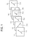
- In a TN (Twisted Nematic) type liquid crystal display panel, as shown in Fig. 1 for both of prior art and the present invention, a pair of
polarization plates liquid crystal cell 14 is interposed is provided. In order to improve the viewing angle characteristics, a TN type liquid crystal display panel wherein tworetardation films retardation film 13 adjacent to theliquid crystal cell 14 is set nearly equal to the direction 4a of liquid crystal molecular orientation on the surface of theliquid crystal cell 14 facing to theretardation film 13. - In the display panel disclosed in the above patent application, each product Δn × d (referred to as retardation) of refractive index anisotropy Δn and thickness d for
retardation films - The viewing angle characteristics for both left-right directions (i.e. horizontal directions) and upper-lower directions (i.e. vertical directions) can be improved to some extent by this prior art. However, the viewing angle characteristics for left-right directions are more important than that for upper-lower directions for a display used in a cockpit of an aircraft. Therefore, strong requirements for a liquid crystal display panel of which viewing angle characteristics for left-right direction are further improved have been raised.
- It is an object of the present invention to provide a liquid crystal display panel of which viewing angle characteristics for left-right directions are further improved in order to respond to those requirements.
- According to the present invention, in a liquid crystal display panel, a TN type liquid crystal cell is interposed between a pair of polarization plates, and a first and a second retardation films each having slow axes nearly orthogonal each other are further interposed between one of the polarization plates and the liquid crystal cell with the second retardation film being positioned on the liquid cryatal side, the product Δn₁ × d₁ of the refractive index anisotropy Δn₁ and the thickness d₁ of the first retardation film is set greater than the product Δn₂ × d₂ of the refractive index anisotropy Δn₂ and the thickness d₂ of the second retardation film.
- In the present invention, it is desirable that the product Δn × d of the refractive index anisotropy Δn and the thickness d of TN type liquid crystal cell is set in the range of 470 ± 200 nm.
- In the present invention, it is desirable that the difference between the product of the refractive index anisotropy and the thickness of the first retardation film and the product of the refractive index anisotropy and the thickness of the second retardation film,

range 0 < R ≦ 50 nm. -
- Fig. 1 is an oblique viewing diagram showing an embodiment of the present invention and a prior art arrangement;
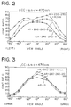
- Fig. 2 is a graph showing an example of the viewing angle characteristics in left-right directions in the embodiment of Fig. 1;
- Fig. 3 is a graph showing an example (corresponding to Fig. 2) of the viewing angle characteristics in upper-lower direction in the embodiment of Fig. 1;
- Fig. 4 is a graph showing another example of the viewing angle characteristics in left-right directions in the embodiment of Fig. 1; and
- Fig. 5 is a graph showing another example (corresponding to Fig. 4) of the viewing angle characteristics in upper-lower directions in the embodiment of Fig. 1.
- The TN type display panel is arranged, like a prior art, as shown in Fig. 1. The duplicated explanation for Fig. 1 is omitted.
- A feature of the present invention is to set the product Δn₁ × d₁ of the refractive index anisotropy Δn₁ and the thickness d₁ of the first retardation film greater than the product Δn₂ × d₂ of the refractive index anisotropy Δn₂ and the thickness d₂ of the second retardation film. By such a setting, as shown by the contrast of vertical axis versus the viewing angle of horizontal axis in Figs. 2 and 4, the viewing angle is expanded and the characteristics are improved compared with the prior art example where the retardation Δn × d is set to the same for two
retardation films 2 and 3. - In Fig. 2, the cases of

- On the other hand, regarding the viewing angle characteristics in upper-lower direction, as shown in Fig. 3 (corresponding to Fig.2) and Fig. 5 (corresponding to Fig.4), the case of ΔR=20 nm is about the same level as or slightly worse than the case of ΔR=0 and the case of ΔR=40 nm is slightly worse than the case of ΔR=0. Actually, from many experiments, it has been confirmed that the viewing angle characteristics in left-right directions improves as ΔR increases while the viewing angle characteristics in upper-lower direction inversely deteriorates as ΔR increases. Practically, it is appreciated that ΔR of 0 < ΔR ≦ 50 nm is desirable.
- Incidentally, it is desirable that the product (retardation) Δn × d of the refractive index anisotropy Δn and the thickness d of TN type
liquid crystal cell 14 be set in the range of 470 ± 200 nm although this is not specified in a prior art example. The reason is that this range of ΔR indicates the best optical characteristics including viewing angle characteristics. Incidentally, this has been well known. - As mentioned above, in the present invention, by setting the retardation ( Δn × d) of the
first retardation film 12 interposed between onepolarization plate 11 and theliquid crystal cell 14 greater than that of thesecond retardation film 13, the viewing angle characteristics in left-right direction can be improved compared with the prior art case where the same retardation value is set for both retardation films. Therefore, an LCD preferable for display used in a cockpit of an aircraft can be provided by the present invention.
Claims (4)
- In a liquid crustal display panel wherein a Twisted Nematic type liquid crystal cell is interposed between a pair of polarization plates and a first and a second retardation films each having slow axes nearly orthogonal each other are interposed between one of the polarization plates and said liquid crystal cell such that said first and second retardation films face to said one of the polarization plates and said liquid crystal cell respectively:
said liquid crystal display panel is characterized in that wherein the product Δn₁ × d₁ of the refractive index anisotropy Δn₁ and the thickness d₁ of said first retardation film is set greater than the product Δn₂ × d₂ of the refractive index anisotropy Δn₂ and the thickness d₂ of said second retardation film. - The liquid crystal display panel according to claim 1, characterized in that the product Δnd of the refractive index anisotropy Δn and the thickness d of said TN type liquid crystal cell is set in the range of 470 ± 200 nm.
- The liquid crystal display panel according to claim 1 or 2, characterized in that the difference between the products of the respective refractive index and thicknesses of said first and second retardation films,

- The liquid crystal display panel according to claim 1 or 2, characterized in that a direction of the slow axis of said second retardation film is arranged to match with the liquid crystal orientation direction on the surface of said liquid crystal cell facing to said second retardation film.
Applications Claiming Priority (3)
| Application Number | Priority Date | Filing Date | Title |
|---|---|---|---|
| JP25336594 | 1994-10-19 | ||
| JP253365/94 | 1994-10-19 | ||
| JP6253365A JPH08122770A (en) | 1994-10-19 | 1994-10-19 | Liquid crystal display element |
Publications (2)
| Publication Number | Publication Date |
|---|---|
| EP0708353A1 true EP0708353A1 (en) | 1996-04-24 |
| EP0708353B1 EP0708353B1 (en) | 2000-04-19 |
Family
ID=17250341
Family Applications (1)
| Application Number | Title | Priority Date | Filing Date |
|---|---|---|---|
| EP95116300A Expired - Lifetime EP0708353B1 (en) | 1994-10-19 | 1995-10-16 | Liquid crystal display panel |
Country Status (6)
| Country | Link |
|---|---|
| US (1) | US5796457A (en) |
| EP (1) | EP0708353B1 (en) |
| JP (1) | JPH08122770A (en) |
| KR (1) | KR100255142B1 (en) |
| DE (1) | DE69516353T2 (en) |
| TW (1) | TW475080B (en) |
Cited By (1)
| Publication number | Priority date | Publication date | Assignee | Title |
|---|---|---|---|---|
| EP0990874A1 (en) * | 1998-10-02 | 2000-04-05 | Mannesmann VDO Aktiengesellschaft | Display device |
Families Citing this family (6)
| Publication number | Priority date | Publication date | Assignee | Title |
|---|---|---|---|---|
| JP2000098393A (en) * | 1998-09-21 | 2000-04-07 | Sharp Corp | Liquid crystal display device |
| JP2002182036A (en) * | 2000-04-06 | 2002-06-26 | Fujitsu Ltd | Viewing angle compensation film and liquid crystal display device |
| US6853413B2 (en) * | 2000-04-18 | 2005-02-08 | Honeywell International Inc. | Polarized display with wide-angle illumination |
| JP3538149B2 (en) * | 2001-01-30 | 2004-06-14 | Nec液晶テクノロジー株式会社 | Reflection type liquid crystal display device and manufacturing method thereof |
| EP1859317B1 (en) * | 2005-03-10 | 2016-06-29 | LG Chem, Ltd. | Vertically alligned liquid crystal display having a wide viewing compensation film using +a-film and +c-film |
| US8814557B2 (en) * | 2010-03-24 | 2014-08-26 | United Technologies Corporation | Die inserts for die casting |
Citations (4)
| Publication number | Priority date | Publication date | Assignee | Title |
|---|---|---|---|---|
| EP0367616A2 (en) * | 1988-11-04 | 1990-05-09 | Matsushita Electric Industrial Co., Ltd. | Optical liquid crystal element |
| JPH02125224A (en) | 1988-11-04 | 1990-05-14 | Matsushita Electric Ind Co Ltd | Electrooptic element |
| US5184236A (en) * | 1990-08-10 | 1993-02-02 | Casio Computer Co., Ltd. | Twisted nematic liquid crystal display device with retardation plates having phase axis direction within 15° of alignment direction |
| JPH06194647A (en) * | 1992-12-25 | 1994-07-15 | Fuji Photo Film Co Ltd | Liquid crystal display element using optical compensation sheet |
Family Cites Families (3)
| Publication number | Priority date | Publication date | Assignee | Title |
|---|---|---|---|---|
| US5396355A (en) * | 1991-06-17 | 1995-03-07 | Seiko Epson Corporation | Optically compensating film, optical compensator and liquid crystal display |
| US5227903A (en) * | 1991-09-20 | 1993-07-13 | Casio Computer Co., Ltd. | Liquid crystal display device with at least one biaxial retardation film having nx >nz >ny |
| US5440413A (en) * | 1991-09-30 | 1995-08-08 | Casio Computer Co., Ltd. | Liquid crystal display device with 2 adjacent biaxial retardation plates having Ny <Nz <Nx |
-
1994
- 1994-10-19 JP JP6253365A patent/JPH08122770A/en active Pending
-
1995
- 1995-08-29 TW TW084109009A patent/TW475080B/en not_active IP Right Cessation
- 1995-10-12 US US08/542,184 patent/US5796457A/en not_active Expired - Lifetime
- 1995-10-16 DE DE69516353T patent/DE69516353T2/en not_active Expired - Fee Related
- 1995-10-16 EP EP95116300A patent/EP0708353B1/en not_active Expired - Lifetime
- 1995-10-17 KR KR1019950035731A patent/KR100255142B1/en not_active IP Right Cessation
Patent Citations (4)
| Publication number | Priority date | Publication date | Assignee | Title |
|---|---|---|---|---|
| EP0367616A2 (en) * | 1988-11-04 | 1990-05-09 | Matsushita Electric Industrial Co., Ltd. | Optical liquid crystal element |
| JPH02125224A (en) | 1988-11-04 | 1990-05-14 | Matsushita Electric Ind Co Ltd | Electrooptic element |
| US5184236A (en) * | 1990-08-10 | 1993-02-02 | Casio Computer Co., Ltd. | Twisted nematic liquid crystal display device with retardation plates having phase axis direction within 15° of alignment direction |
| JPH06194647A (en) * | 1992-12-25 | 1994-07-15 | Fuji Photo Film Co Ltd | Liquid crystal display element using optical compensation sheet |
Non-Patent Citations (1)
| Title |
|---|
| PATENT ABSTRACTS OF JAPAN vol. 018, no. 541 (P - 1813) 14 October 1994 (1994-10-14) * |
Cited By (3)
| Publication number | Priority date | Publication date | Assignee | Title |
|---|---|---|---|---|
| EP0990874A1 (en) * | 1998-10-02 | 2000-04-05 | Mannesmann VDO Aktiengesellschaft | Display device |
| US6522381B1 (en) | 1998-10-02 | 2003-02-18 | Mannesmann Vdo Ag | Display device having pointer and electrooptic display |
| US6674497B2 (en) | 1998-10-02 | 2004-01-06 | Mannesmann Vdo Ag | Electrooptic display device |
Also Published As
| Publication number | Publication date |
|---|---|
| TW475080B (en) | 2002-02-01 |
| DE69516353T2 (en) | 2000-10-12 |
| EP0708353B1 (en) | 2000-04-19 |
| KR960015018A (en) | 1996-05-22 |
| KR100255142B1 (en) | 2000-05-01 |
| JPH08122770A (en) | 1996-05-17 |
| DE69516353D1 (en) | 2000-05-25 |
| US5796457A (en) | 1998-08-18 |
Similar Documents
| Publication | Publication Date | Title |
|---|---|---|
| EP0352724B1 (en) | A liquid crystal display device | |
| EP0487359B1 (en) | A liquid crystal display | |
| EP0393191B1 (en) | Liquid crystal display | |
| US6285430B1 (en) | Liquid crystal display device | |
| US7518680B2 (en) | Active matrix type liquid crystal display | |
| EP0899605A3 (en) | Liquid crystal display device | |
| EP0774682A2 (en) | Normally white twisted nematic LCD with positive and negative phase retarders | |
| EP0793134B1 (en) | Liquid crystal display having alternating cuts in electrodes | |
| CA2148156A1 (en) | Lcd with a pair of retardation films on one side of liquid crystal layer | |
| KR20080067703A (en) | Phase difference film, polarization film, liquid crystal display unit, and method of designing phase difference film | |
| EP0372973A3 (en) | Liquid crystal display device comprising improved viewing angle characteristics | |
| EP0350063A2 (en) | Liquid crystal display device | |
| US20120236232A1 (en) | Liquid crystal display | |
| US5448386A (en) | Optical liquid crystal element | |
| EP0350062B1 (en) | Liquid crystal display device | |
| JPH04153622A (en) | Tn type liquid crystal display element | |
| EP0708353A1 (en) | Liquid crystal display panel | |
| EP0871059A3 (en) | Liquid crystal display device | |
| US6587171B1 (en) | Angle of view of a LCD screen by a novel birefringent film stacking | |
| JPH10239683A (en) | Reflective-type liquid crystal; display device | |
| JP2573383B2 (en) | Liquid crystal display | |
| KR100697570B1 (en) | Normally-white tn-mode lcd device | |
| JPH05157913A (en) | Phase difference film and liquid crystal display element | |
| JP2870860B2 (en) | Liquid crystal display device | |
| US20050073635A1 (en) | Liquid crystal display device |
Legal Events
| Date | Code | Title | Description |
|---|---|---|---|
| PUAI | Public reference made under article 153(3) epc to a published international application that has entered the european phase |
Free format text: ORIGINAL CODE: 0009012 |
|
| 17P | Request for examination filed |
Effective date: 19951016 |
|
| AK | Designated contracting states |
Kind code of ref document: A1 Designated state(s): DE FR GB NL |
|
| RAP1 | Party data changed (applicant data changed or rights of an application transferred) |
Owner name: HOSIDEN AND PHILIPS DISPLAY CORPORATION |
|
| GRAG | Despatch of communication of intention to grant |
Free format text: ORIGINAL CODE: EPIDOS AGRA |
|
| GRAG | Despatch of communication of intention to grant |
Free format text: ORIGINAL CODE: EPIDOS AGRA |
|
| GRAH | Despatch of communication of intention to grant a patent |
Free format text: ORIGINAL CODE: EPIDOS IGRA |
|
| 17Q | First examination report despatched |
Effective date: 19990812 |
|
| GRAH | Despatch of communication of intention to grant a patent |
Free format text: ORIGINAL CODE: EPIDOS IGRA |
|
| GRAA | (expected) grant |
Free format text: ORIGINAL CODE: 0009210 |
|
| AK | Designated contracting states |
Kind code of ref document: B1 Designated state(s): DE FR GB NL |
|
| REF | Corresponds to: |
Ref document number: 69516353 Country of ref document: DE Date of ref document: 20000525 |
|
| ET | Fr: translation filed | ||
| PLBE | No opposition filed within time limit |
Free format text: ORIGINAL CODE: 0009261 |
|
| STAA | Information on the status of an ep patent application or granted ep patent |
Free format text: STATUS: NO OPPOSITION FILED WITHIN TIME LIMIT |
|
| 26N | No opposition filed | ||
| PG25 | Lapsed in a contracting state [announced via postgrant information from national office to epo] |
Ref country code: NL Free format text: LAPSE BECAUSE OF NON-PAYMENT OF DUE FEES Effective date: 20010501 |
|
| NLV4 | Nl: lapsed or anulled due to non-payment of the annual fee |
Effective date: 20010501 |
|
| REG | Reference to a national code |
Ref country code: GB Ref legal event code: 732E |
|
| REG | Reference to a national code |
Ref country code: FR Ref legal event code: TP |
|
| REG | Reference to a national code |
Ref country code: FR Ref legal event code: CD |
|
| REG | Reference to a national code |
Ref country code: GB Ref legal event code: IF02 |
|
| REG | Reference to a national code |
Ref country code: GB Ref legal event code: 746 Effective date: 20020911 |
|
| REG | Reference to a national code |
Ref country code: FR Ref legal event code: D6 |
|
| PGFP | Annual fee paid to national office [announced via postgrant information from national office to epo] |
Ref country code: FR Payment date: 20031027 Year of fee payment: 9 |
|
| PGFP | Annual fee paid to national office [announced via postgrant information from national office to epo] |
Ref country code: GB Payment date: 20031031 Year of fee payment: 9 |
|
| PGFP | Annual fee paid to national office [announced via postgrant information from national office to epo] |
Ref country code: DE Payment date: 20031215 Year of fee payment: 9 |
|
| PG25 | Lapsed in a contracting state [announced via postgrant information from national office to epo] |
Ref country code: GB Free format text: LAPSE BECAUSE OF NON-PAYMENT OF DUE FEES Effective date: 20041016 |
|
| PG25 | Lapsed in a contracting state [announced via postgrant information from national office to epo] |
Ref country code: DE Free format text: LAPSE BECAUSE OF NON-PAYMENT OF DUE FEES Effective date: 20050503 |
|
| GBPC | Gb: european patent ceased through non-payment of renewal fee |
Effective date: 20041016 |
|
| PG25 | Lapsed in a contracting state [announced via postgrant information from national office to epo] |
Ref country code: FR Free format text: LAPSE BECAUSE OF NON-PAYMENT OF DUE FEES Effective date: 20050630 |
|
| REG | Reference to a national code |
Ref country code: FR Ref legal event code: ST |