EP0704969B1 - Astable multivibrators - Google Patents
Astable multivibrators Download PDFInfo
- Publication number
- EP0704969B1 EP0704969B1 EP95115289A EP95115289A EP0704969B1 EP 0704969 B1 EP0704969 B1 EP 0704969B1 EP 95115289 A EP95115289 A EP 95115289A EP 95115289 A EP95115289 A EP 95115289A EP 0704969 B1 EP0704969 B1 EP 0704969B1
- Authority
- EP
- European Patent Office
- Prior art keywords
- output
- inverter
- input signal
- level
- signal
- Prior art date
- Legal status (The legal status is an assumption and is not a legal conclusion. Google has not performed a legal analysis and makes no representation as to the accuracy of the status listed.)
- Expired - Lifetime
Links
Images


Classifications
-
- H—ELECTRICITY
- H03—ELECTRONIC CIRCUITRY
- H03K—PULSE TECHNIQUE
- H03K3/00—Circuits for generating electric pulses; Monostable, bistable or multistable circuits
- H03K3/02—Generators characterised by the type of circuit or by the means used for producing pulses
- H03K3/26—Generators characterised by the type of circuit or by the means used for producing pulses by the use, as active elements, of bipolar transistors with internal or external positive feedback
- H03K3/28—Generators characterised by the type of circuit or by the means used for producing pulses by the use, as active elements, of bipolar transistors with internal or external positive feedback using means other than a transformer for feedback
- H03K3/281—Generators characterised by the type of circuit or by the means used for producing pulses by the use, as active elements, of bipolar transistors with internal or external positive feedback using means other than a transformer for feedback using at least two transistors so coupled that the input of one is derived from the output of another, e.g. multivibrator
- H03K3/282—Generators characterised by the type of circuit or by the means used for producing pulses by the use, as active elements, of bipolar transistors with internal or external positive feedback using means other than a transformer for feedback using at least two transistors so coupled that the input of one is derived from the output of another, e.g. multivibrator astable
-
- H—ELECTRICITY
- H03—ELECTRONIC CIRCUITRY
- H03K—PULSE TECHNIQUE
- H03K3/00—Circuits for generating electric pulses; Monostable, bistable or multistable circuits
- H03K3/02—Generators characterised by the type of circuit or by the means used for producing pulses
- H03K3/027—Generators characterised by the type of circuit or by the means used for producing pulses by the use of logic circuits, with internal or external positive feedback
- H03K3/03—Astable circuits
-
- Y—GENERAL TAGGING OF NEW TECHNOLOGICAL DEVELOPMENTS; GENERAL TAGGING OF CROSS-SECTIONAL TECHNOLOGIES SPANNING OVER SEVERAL SECTIONS OF THE IPC; TECHNICAL SUBJECTS COVERED BY FORMER USPC CROSS-REFERENCE ART COLLECTIONS [XRACs] AND DIGESTS
- Y10—TECHNICAL SUBJECTS COVERED BY FORMER USPC
- Y10S—TECHNICAL SUBJECTS COVERED BY FORMER USPC CROSS-REFERENCE ART COLLECTIONS [XRACs] AND DIGESTS
- Y10S331/00—Oscillators
- Y10S331/03—Logic gate active element oscillator
Definitions
- the present invention relates to high frequency oscillators, and more particularly to astable multivibrators.
- astable multivibrators have been used as oscillators in 4 bit or 8 bit micro-computers and as portable timekeeping devices.
- the driving oscillator in DC-DC converter circuits it is desirable to generate relatively high frequencies.
- Present technology dictates that integrated oscillators be of the resistance-capacitance type since inductive elements cannot be fabricated in integrated form.
- the operating frequency thereof is determined by resistors R and capacitors C, and most of the capacitors have fixed capacitance value.
- the capacitor should be fabricated in a size capable of minimizing the effect of parasitic capacitance. If the capacitor is fabricated in a larger size in order to increase the capacitance thereof, this may cause an increase in power consumption.
- an integrated RC oscillator has a problem of deteriorating high frequency oscillation performance due to the effect of the parasitic capacitance generated within the integrated circuit as well as a small feedback resistance to an input part.
- CMOS Complementary Metal Oxide Semiconductor
- Figure 1 of the accompanying diagrammatic drawings shows a circuit construction of a conventional astable multivibrator.
- Figure 2 is a circuit diagram of another design of astable multivibrator.
- Figure 3 is a detailed circuit diagram of Figure 2.
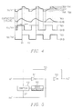
- Figure 4 is a voltage waveform diagram illustrating operation of the multivibrator of Figure 2 as compared with that of Figure 1.
- a variable resistor 17 is connected between an input signal Xi and a feedback signal Xo, and the input signal Xi is connected to an output signal Xp through first and second inverters 11 and 13.
- a capacitor 15 is connected between the input and output signals Xi and Xp, and the output of the first inverter 11 (or the input of the second inverter 13) is coupled to the feedback signal Xo.
- the feedback signal Xo When a supply voltage is applied to the circuit, the feedback signal Xo has a CMOS logic level opposite to those of the input and output signals Xi and Xp. If the CMOS logic level is higher than the switching threshold voltage Vst of the first inverter 11, it goes to a logic "high” level, and otherwise, it goes to a logic “low” level.
- the first and second inverters 11 and 13 serve as amplifiers, and the voltage of the input signal Xi increases by the feedback signal Xo.
- the voltage of the input signal Xi begins to be decreased through the variable resistor 17. If the voltage of the input signal Xi drops below the switching threshold voltage Vst of the first inverter 11, the output voltage of the first inverter 11 goes to the logic "high” level, and the output voltage of the second inverter 13 goes to the logic "low” level. Consequentially, the voltage of the input signal Xi is affected by the output signal Xp of logic "low” level through the capacitor 15 and is thereby lowered much more. At this time, the feedback signal Xo of logic "high” level increases the voltage of the input signal Xi through the variable resistor 17 from the time t2.
- the variable resistor 17 serves as a factor determining how fast the input signal Xi which is affected by the voltage level of the feedback signal Xo swings from the logic "high” level to the logic “low” level or from the logic "low” level to the logic “high” level. That is, the variable resistor 17 determines the charge-discharge time of the capacitor 15, and consequentially becomes the factor for specifying the high frequency oscillation cycle of the vibrator.
- the resistance value of the variable resistor 17 should be small within a predetermined range.
- the input signal Xi should have a desirable voltage operating range VDD + Vst to Vst - VDD.
- the charge or discharge operation to the capacitor 15 begins at Vx or -Vx, i.e. before the input signal Xi reaches VDD + Vst or Vst - Vdd. That is, the input signal Xi does not have the voltage operating range of VDD + Vst ⁇ Vst -VDD.
- the resistance value of the variable resistor 17 sufficiently high, there occurs a problem of deteriorating the high frequency oscillation performance, while improving the above problem of narrow voltage operating range.
- US patent no. 3851277 describes a high frequency multivibrator in which three inverters are serially coupled to one another. Each inverter consists of a pair of complementary MOS transistors coupled in series between ground potential and a negative power supply voltage. A timing circuit includes a capacitor connected across the first two inverters and a resistor connected across all three inverters.
- a variable resistor 27 is connected between an input signal Xi' and a feedback signal Xo'.
- First and second inverters 21 and 23 are serially connected between the input signal Xi' and an output signal Xp', and a capacitor 25 is connected between the input and output signals Xi' and Xp' and in parallel with the first and second inverters 21 and 23.
- a CMOS type capacitor is employed herein for the capacitor 25.
- a delay 20 for delaying an output signal Xd' of the first inverter 21 for a predetermined time ⁇ is connected between the output of the first inverter 21 and the feedback signal Xo'.
- the delay 20 can be fabricated by serially connecting even numbers of inverters corresponding to the required delay time ⁇ .
- the circuit can also be implemented by using a CMOS transmission gate 32 used as an internal resistor between the input and feedback signals Xi' and Xo' as shown in Figure 3. As the length of the transmission gate is much larger than the width thereof, the transmission gate 32 has a negligible resistance value.
- buffers 34 and 36 coupled to a node connected to the output of the second inverter 33 and to the capacitor 35 can also be employed for shaping the output signal Xp'.
- the input, feedback and output signals Xi', Xo' and Xp' respectively maintain logic "low”, "high” and “low” levels at the beginning of the application.
- the feedback signal Xo' goes to the logic "high” level after the lapse of the delay time ⁇ from the application of the supply voltage.
- the voltage of the input signal Xi' begins to increase by the feedback signal Xo' of logic "high” level. If the voltage of the input signal Xi' increases above the switching threshold voltage Vst of the first inverter 21 or 31, the output signal Xd' of the first inverter 21 or 31 goes to logic "low” level and the output voltage of the second inverter 23 or 33, that is, the voltage of the output signal Xp' goes to logic "high” level.
- the output signal Xd' of logic "low” level is time-delayed by ⁇ through the delay 20 or 30, and then is output as the feedback signal Xo'.
- the feedback signal Xo' goes to the logic "low" level.
- the voltage of the input signal Xi' acceleratedly increases to the level of VDD + Vst in response to the increase of the voltage level of the output signal Xp' (whereas the voltage of the input signal Xi begins to drop before reaching the level of VDD + Vst in the circuit of Figure 1).
- the voltage of the input signal Xi' begins to drop with the transition of the feedback signal Xo' to the logic "low” level. If the voltage of the input signal Xi' decreases below the switching threshold voltage Vst of the first inverter 21 or 31, the output signal Xd' of the first inverter 21 or 31 goes to logic "high” level and the output signal Xp' goes to logic "low” level. As aforementioned, the feedback signal Xo' goes to the logic "high” level after the lapse of the delay time ⁇ from the time t2. Thus, during this delay time ⁇ , the voltage of the input signal Xi' acceleratedly decreases to the level of Vst - VDD in response to the voltage drop of the output signal Xp'.
- the delay time ⁇ ensures that the high frequency input signal Xi' has a voltage operating range of VDD + Vst ⁇ Vst - VDD, thus solving the problem of the conventional circuit of Figure 1 that the input signal Xi cannot have a wide voltage operating range required in a normal operation. Therefore, it is possible to ensure a desired voltage operating range even though the resistance value of the resistor 27 or 37 is set as to as low a value as possible, so as to make the high frequency oscillation cycle faster.
- the input signal Xi in the conventional circuit has a voltage of 3.799V (corresponds to the Vx level in the waveform of Figure 4) and a frequency of 31.7MHz
- the input signal Xi' in Figure 3 has a voltage of 5.637V (corresponds to the VDD + Vst level) and a frequency of 35.9MHz.
- Preferred embodiments of the present invention aim to provide an improved astable multivibrator capable of generating a high frequency output signal having a stable and wide voltage operating range even though the resistance value determining the charge-discharge time of a capacitor is small.
- a multivibrator comprising:
- the output of one of the amplification means (51) is connected to the feedback signal node.
- the plurality of amplification means comprises a first inverter (51) having an input terminal connected to the input signal node, and a second inverter (53) having input and output terminals connected between an output terminal of the first inverter and the output signal node.
- the edge detection means comprises square wave generation means (70-1) for shaping the output signal of the first inverter (61) into a square wave, a delay means (70-2 to 70-4) for delaying the output signal of the first inverter (61) for a predetermined time, and NAND and NOR gates (70-5, 70-6) for receiving the output signals of the square wave generation means (70-1) and the delay means (70-2 to 70-4).
- the delay means (70-2 to 70-4) comprises an odd number of inverters.
- the square wave generation means (70-1) comprises at least one inverter.
- the switching means (60) comprises a plurality of transmission gates (60A-2 to 60B-2) serially connected to one another, each composed of an NMOS transistor and a PMOS transistor.
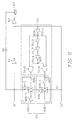
- Figure 5 is a circuit diagram showing an astable multivibrator according to another embodiment of the present invention
- Figure 6 is an example of a detailed circuit diagram of Figure 5.
- Figure 7 shows a voltage waveform diagram of each node in the edge detector of Figure 5.
- the astable multivibrator comprises a pair of inverting amplifiers 51 and 53 connected between an input signal Xi'' and an output signal Xp", a capacitor 55 connected between the input and output signals Xi'' and Xp" and in parallel with the amplifiers 51 and 53, an edge detector 50 connected to a feedback signal Xo", for detecting the variation of the voltage level of the feedback signal Xo' which has passed through the amplifier 51, a resistor 57 connected between the input and feedback signals Xi'' and Xo'', and a switch 40 connected between the input signal Xi'' and the resistor 57, for switching the connection state therebetween in response to the output signal of the edge detector 50.
- first and second inverters 61 and 63 are serially connected between a first signal node and a third signal node, and a capacitor 65 is connected in parallel with the first and second inverters 61 and 63.
- An edge detector 70 detects the first and second edge pulses of a feedback signal Xo'' output from a connection node between the first and second inverters 61 and 63.
- a resistor 67 is connected to an input node of the edge detector 70 at its one end.
- a switch 60 is connected between the first signal node and the other end of the resistor 67, for isolating the path therebetween during the reception of the first and second edge detection pulses from the edge detector 70.
- the edge detector 70 comprises a square wave generator composed of a third inverter 70-1, delay means composed of fourth, fifth and sixth inverters 70-2, 70-3 and 70-4 serially connected to one another for delaying the output of the square wave generator for a predetermined time, and a NAND gate 70-5 for NANDing the output of the third inverter 70-1 and the output of the delay means and then outputting the first edge detection pulse, i.e. the rising edge pulse, and a NOR gate 70-6 for NORing the output of the third inverter 70-1 and the output of the delay means and then outputting the second edge detection pulse, i.e. the falling edge pulse.
- the switch 60 comprises first and second transmission gates 60A and 60B to be switched on respectively responsive to the first and second edge detection pulses output from the NAND gate 70-5 and the NOR gate 70-6.
- 60A-2 and 60B-2 are typical transmission gates, each composed of an NMOS transistor and a PMOS transistor
- 60A-1 and 60B-1 are inverters for inverting the first and second edge detection pulses and driving the control electrodes of the PMOS transistors in the transmission gates 60A-2 and 60B-2.
- the operation of opening/isolating the connection between the input signal Xi'' and the resistor 67 in response to the output of the edge detector 70 will now be described. If the feedback signal Xo'' is applied to the third inverter 70-1, the inverted signal is output to a node N24, shown as A in Figure 7. The signal thus obtained is inverted and delayed for a predetermined time T1 through the fourth, fifth and sixth inverters 70-2, 70-3 and 70-4, shown as B in Figure 7, and then is output to a node N25. The outputs of the nodes N24 and N25 are commonly applied to the NAND gate 70-5 and NOR gate 70-6, and the signals shown as C and D of Figure 7 are then output to the nodes N26 and N27.
- the NMOS gate electrode of the first transmission gate 60A is coupled to the output line of the NAND gate 70-5 and the PMOS gate electrode thereof to the output of the NAND gate 70-5 through a seventh inverter 60A-1, whereby the first transmission gate 60A is turned on when the output signal of the NAND gate 70-5 is at a logic "high” level.
- the NMOS gate electrode of the second transmission gate 60B is coupled to the output of the NOR gate 70-6 through an eighth inverter 60B-1 and the PMOS gate electrode thereof to the output line of the NOR gate 70-6, whereby the second transmission gate 60B is turned on when the output signal of the NOR gate 70-6 is at a logic "low” level.
- the transmission gate 60B is turned off, and during the delay time T2, the first transmission gate 60A is turned off.
- the effect of the resistance value of the resistor 67 which is to be fed back to the input signal Xi'' is eliminated. Therefore, the input signal swings sufficiently to the logic "high” level or to the logic “low” level, outputting the output signal Xp" of high frequency with correct cycle.
- the input signal Xi" of logic "low” level affects the output signal Xp" to be dropped much more to the logic “low” level. Such a step will be repeated until the output signal Xp" becomes 0V. After the output signal Xp" becomes 0V, the input signal Xi" remains at logic "low” level while the switch 60 is turned off by the edge detector 70. After the lapse of a predetermined delay time by the edge detector 70, the switch 60 is turned on, and the capacitor 65 is charged by the feedback current passed through the resistor 67 in response to the level variation of the feedback signal Xo'' which has passed through the first inverter 61.
- the edge detector 70 detects the level variation of the feedback signal Xo'' which has passed through the first inverter 61, and the switch 60 is thereby turned off. At this time, the input signal Xi" becomes higher than the switching threshold voltage by the first inverter 61, switch 60 and edge detector 70.
- Such a small variation of the input signal Xi" is amplified through the first and second inverters 61 and 63 and affects the output signal Xp".
- the input signal Xi" is varied again through the capacitor 65 by as much as the variation of the output signal Xp".
- Such an operation is repeated until the output signal Xp" reaches the VDD level.
- the input signal Xi" maintains the logic "high” level for the time delayed by the edge detector 70.
- the switch 60 is turned on again, and the step of discharging the potential of the input signal Xi" from the capacitor 65 is repeated.
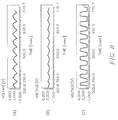
- Figure 8 is a voltage waveform diagram according to the result of a simulation using a conventional circuit.
- A, B and C show the waveforms of the input, feedback and output signals Xi, Xo, and Xp, respectively.
- the input signal Xi cannot have sufficient amplitude by the effect of the feedback resistance from the feedback signal Xo, resulting in the generation of a high frequency waveform with incorrect cycle.
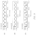
- Figure 9 is a voltage waveform diagram according to the result of such a simulation using an example of the present invention.
- A, B and C show the waveforms of the input, feedback and output signals Xi", Xo", and Xp", respectively.
- the input signal Xi" has sufficient amplitude by being isolated from the effect of the feedback resistance from the output signal of the first inverter, resulting in the generation of a high frequency waveform with correct cycle.
- the major advantage of an astable multivibrator according to the present invention is the ability to enhance the high frequency oscillation performance and to generate high frequency output signals with a desired voltage operating range. In addition, it is possible to obtain high frequency output waveforms with correct cycles by excluding the effect of the feedback current, thus enhancing the oscillation performance and reliability of the astable multivibrator.
Landscapes
- Engineering & Computer Science (AREA)
- Power Engineering (AREA)
- Manipulation Of Pulses (AREA)
- Pulse Circuits (AREA)
Description
| 100 | 50 KΩ | 10 KΩ | 4 | 2 KΩ | 1.7 KΩ | 1.4 KΩ | 1.1 | 0 KΩ | ||
| Figure I (prior art) | Xi[V] | 5.637 | 5.635 | 5.618 | 5.322 | 4.490 | 4.189 | 3.799 | No Vibration | No Vibration |
| [MHz] | 1.6 | 3.0 | 11.4 | 21.7 | 29.7 | 31.5 | 31.7 | No vibration | No Vibration | |
| Figure 3 (invention) | Xi'[V] | 5.646 | 5.644 | 5.642 | 5.640 | 5.639 | 5.638 | 5.637 | 5.635 | 5.595 |
| [MHz] | 1.7 | 3.1 | 11.6 | 21.7 | 31.2 | 33.3 | 35.9 | 38.5 | 53.0 |
Claims (7)
- A multivibrator comprising:a plurality of amplification means (51,53) serially connected between an input signal node and an output signal node;capacitor means (55) connected in parallel with the plurality of amplification means (51,53); andresistor means (57) disposed between the input signal node and a feedback signal node to which a feedback signal Xo" logic-converted from the input signal node is supplied;characterized by edge detection means (50) for detecting an edge of the feedback signal Xo"; andswitching means (40) for switching the connection of the resistor means (57) in response to an output signal of the edge detection means (50) to isolate the path between the input signal node and the feedback node for a predetermined time after detection of an edge of the feedback signal Xo".
- A multivibrator according to claim 1, wherein the output of one of the amplification means (51) is connected to the feedback signal node.
- A multivibrator according to claim 1 or claim 2, wherein the plurality of amplification means comprises a first inverter (51) having an input terminal connected to the input signal node, and a second inverter (53) having input and output terminals connected between an output terminal of the first inverter and the output signal node.
- A multivibrator according to claim 3, wherein the edge detection means comprises square wave generation means (70-1) for shaping the output signal of the first inverter (61) into a square wave, a delay means (70-2 to 70-4) for delaying the output signal of the first inverter (61) for a predetermined time, and NAND and NOR gates (70-5, 70-6) for receiving the output signals of the square wave generation means (70-1) and the delay means (70-2 to 70-4).
- A multivibrator according to claim 4, wherein the delay means (70-2 to 70-4) comprises an odd number of inverters.
- A multivibrator according to claim 4 or 5, wherein the square wave generation means (70-1) comprises at least one inverter.
- A multivibrator according to any preceding claim, wherein the switching means (60) comprises a plurality of transmission gates (60A-2 to 60B-2) serially connected to one another, each composed of an NMOS transistor and a PMOS transistor.
Applications Claiming Priority (6)
| Application Number | Priority Date | Filing Date | Title |
|---|---|---|---|
| KR19940024755 | 1994-09-29 | ||
| KR9424755 | 1994-09-29 | ||
| KR9426194 | 1994-10-13 | ||
| KR19940026194 | 1994-10-13 | ||
| KR9434590 | 1994-12-16 | ||
| KR1019940034590A KR0167612B1 (en) | 1994-09-29 | 1994-12-16 | Unstable Multivibrator |
Publications (2)
| Publication Number | Publication Date |
|---|---|
| EP0704969A1 EP0704969A1 (en) | 1996-04-03 |
| EP0704969B1 true EP0704969B1 (en) | 1998-10-28 |
Family
ID=27349102
Family Applications (1)
| Application Number | Title | Priority Date | Filing Date |
|---|---|---|---|
| EP95115289A Expired - Lifetime EP0704969B1 (en) | 1994-09-29 | 1995-09-28 | Astable multivibrators |
Country Status (5)
| Country | Link |
|---|---|
| US (1) | US5712600A (en) |
| EP (1) | EP0704969B1 (en) |
| JP (1) | JP3093140B2 (en) |
| KR (1) | KR0167612B1 (en) |
| DE (1) | DE69505623T2 (en) |
Families Citing this family (2)
| Publication number | Priority date | Publication date | Assignee | Title |
|---|---|---|---|---|
| KR100604983B1 (en) * | 2004-06-14 | 2006-07-31 | 삼성전자주식회사 | Capacitance multiplier with low power consumption |
| JP7599588B2 (en) * | 2022-01-31 | 2024-12-13 | 三菱電機株式会社 | Oscillator Circuit |
Family Cites Families (19)
| Publication number | Priority date | Publication date | Assignee | Title |
|---|---|---|---|---|
| US3302132A (en) * | 1965-10-01 | 1967-01-31 | Gen Dynamics Corp | Bistable multivibrator with self-triggering circuit utilizing level detector tunnel diodes |
| US3517339A (en) * | 1966-03-21 | 1970-06-23 | Vidar Corp | Voltage to frequency converter having symmetrical waveshape output with fundamental frequency proportional to input signal |
| US3568086A (en) * | 1969-05-29 | 1971-03-02 | Eg & G Int | Oscillator system |
| US3851277A (en) * | 1972-12-27 | 1974-11-26 | Tokyo Shibaura Electric Co | Astable multivibrator using insulated-gate field effect transistors |
| US3821470A (en) * | 1973-05-21 | 1974-06-28 | Zenith Radio Corp | Phase correction for horizontal oscillator in cmos form |
| JPS5235566A (en) * | 1975-09-12 | 1977-03-18 | Toshiba Corp | Pulse generator equipment |
| US4301427A (en) * | 1977-07-30 | 1981-11-17 | Tokyo Shibaura Denki Kabushiki Kaisha | Astable MOS FET multivibrator |
| JPS5448551U (en) * | 1977-09-09 | 1979-04-04 | ||
| JPS5917892B2 (en) * | 1978-02-03 | 1984-04-24 | ホーチキ株式会社 | multi vibrator |
| JPS5538784A (en) * | 1978-09-12 | 1980-03-18 | Mitsubishi Electric Corp | Oscillation circuit |
| JPS5673919A (en) * | 1979-11-22 | 1981-06-19 | Toshiba Corp | Oscillation circuit |
| JPS59178014A (en) * | 1983-03-29 | 1984-10-09 | Nissan Motor Co Ltd | Oscillation circuit |
| JPS59228412A (en) * | 1983-06-09 | 1984-12-21 | Toshiba Corp | Multivibrator |
| US4714901A (en) * | 1985-10-15 | 1987-12-22 | Gould Inc. | Temperature compensated complementary metal-insulator-semiconductor oscillator |
| JP2603627B2 (en) * | 1987-01-27 | 1997-04-23 | 松下電工株式会社 | High frequency magnetic therapy device using ring oscillator with variable oscillation frequency |
| US4987389A (en) * | 1990-04-02 | 1991-01-22 | Borg-Warner Automotive, Inc. | Lockproof low level oscillator using digital components |
| JPH0455829U (en) * | 1990-09-19 | 1992-05-13 | ||
| JPH04207627A (en) * | 1990-11-30 | 1992-07-29 | Mitsubishi Electric Corp | Oscillation circuit |
| JPH07131301A (en) * | 1993-11-01 | 1995-05-19 | Nippon Precision Circuits Kk | Cr oscillation circuit |
-
1994
- 1994-12-16 KR KR1019940034590A patent/KR0167612B1/en not_active Expired - Lifetime
-
1995
- 1995-09-28 EP EP95115289A patent/EP0704969B1/en not_active Expired - Lifetime
- 1995-09-28 DE DE69505623T patent/DE69505623T2/en not_active Expired - Lifetime
- 1995-09-29 JP JP07252470A patent/JP3093140B2/en not_active Expired - Fee Related
- 1995-09-29 US US08/536,922 patent/US5712600A/en not_active Expired - Lifetime
Also Published As
| Publication number | Publication date |
|---|---|
| US5712600A (en) | 1998-01-27 |
| JPH08116239A (en) | 1996-05-07 |
| JP3093140B2 (en) | 2000-10-03 |
| DE69505623D1 (en) | 1998-12-03 |
| KR0167612B1 (en) | 1999-03-20 |
| DE69505623T2 (en) | 1999-06-17 |
| KR960012712A (en) | 1996-04-20 |
| EP0704969A1 (en) | 1996-04-03 |
Similar Documents
| Publication | Publication Date | Title |
|---|---|---|
| EP0053014B1 (en) | Clock generator circuit | |
| US4874971A (en) | Edge-sensitive dynamic switch | |
| KR890005227B1 (en) | Ping oscillator with delay element and potential pulling circuit | |
| US4920282A (en) | Dynamic latch circuit for preventing short-circuit current from flowing during absence of clock pulses when under test | |
| US6388479B1 (en) | Oscillator based power-on-reset circuit | |
| KR100440448B1 (en) | Semiconductor integrated circuit device capable of securing time delay insensitive to temperature variation | |
| US6016070A (en) | Pulse extending circuit | |
| US20040051579A1 (en) | Signal generator for charge pump in an integrated circuit | |
| US6518848B2 (en) | Oscillation stop detection circuit | |
| EP0232038B1 (en) | Semiconductor integrated circuit with detection circuit for address signal change | |
| US6346841B2 (en) | Pulse generator | |
| EP0858160B1 (en) | Voltage controlled oscillator | |
| US6081137A (en) | Frequency detecting circuit | |
| US6320420B1 (en) | Domino logic element realizing high speed dynamic logic circuit | |
| US5712600A (en) | Astable multivibrator | |
| KR0168079B1 (en) | Clock generating apparatus | |
| US6320443B1 (en) | RC delay time stabilizing circuit | |
| US5923201A (en) | Clock signal generating circuit | |
| US5258659A (en) | Timed delayed digital signal producing circuit | |
| US7236038B2 (en) | Pulse generator and method for pulse generation thereof | |
| US5808484A (en) | Method and apparatus for detecting changes in a clock signal to static states | |
| US6181214B1 (en) | Voltage tolerant oscillator input cell | |
| JP2874613B2 (en) | Analog delay circuit | |
| KR0137298B1 (en) | High frequency oscillation circuit | |
| US5424661A (en) | Sensor circuit |
Legal Events
| Date | Code | Title | Description |
|---|---|---|---|
| PUAI | Public reference made under article 153(3) epc to a published international application that has entered the european phase |
Free format text: ORIGINAL CODE: 0009012 |
|
| 17P | Request for examination filed |
Effective date: 19951009 |
|
| AK | Designated contracting states |
Kind code of ref document: A1 Designated state(s): DE FR GB |
|
| 17Q | First examination report despatched |
Effective date: 19970430 |
|
| GRAG | Despatch of communication of intention to grant |
Free format text: ORIGINAL CODE: EPIDOS AGRA |
|
| GRAG | Despatch of communication of intention to grant |
Free format text: ORIGINAL CODE: EPIDOS AGRA |
|
| GRAH | Despatch of communication of intention to grant a patent |
Free format text: ORIGINAL CODE: EPIDOS IGRA |
|
| GRAH | Despatch of communication of intention to grant a patent |
Free format text: ORIGINAL CODE: EPIDOS IGRA |
|
| GRAA | (expected) grant |
Free format text: ORIGINAL CODE: 0009210 |
|
| AK | Designated contracting states |
Kind code of ref document: B1 Designated state(s): DE FR GB |
|
| REF | Corresponds to: |
Ref document number: 69505623 Country of ref document: DE Date of ref document: 19981203 |
|
| ET | Fr: translation filed | ||
| PLBE | No opposition filed within time limit |
Free format text: ORIGINAL CODE: 0009261 |
|
| STAA | Information on the status of an ep patent application or granted ep patent |
Free format text: STATUS: NO OPPOSITION FILED WITHIN TIME LIMIT |
|
| 26N | No opposition filed | ||
| REG | Reference to a national code |
Ref country code: GB Ref legal event code: IF02 |
|
| PGFP | Annual fee paid to national office [announced via postgrant information from national office to epo] |
Ref country code: DE Payment date: 20130820 Year of fee payment: 19 |
|
| PGFP | Annual fee paid to national office [announced via postgrant information from national office to epo] |
Ref country code: GB Payment date: 20130823 Year of fee payment: 19 |
|
| PGFP | Annual fee paid to national office [announced via postgrant information from national office to epo] |
Ref country code: FR Payment date: 20130920 Year of fee payment: 19 |
|
| REG | Reference to a national code |
Ref country code: DE Ref legal event code: R119 Ref document number: 69505623 Country of ref document: DE |
|
| GBPC | Gb: european patent ceased through non-payment of renewal fee |
Effective date: 20140928 |
|
| REG | Reference to a national code |
Ref country code: DE Ref legal event code: R119 Ref document number: 69505623 Country of ref document: DE Effective date: 20150401 |
|
| REG | Reference to a national code |
Ref country code: FR Ref legal event code: ST Effective date: 20150529 |
|
| PG25 | Lapsed in a contracting state [announced via postgrant information from national office to epo] |
Ref country code: DE Free format text: LAPSE BECAUSE OF NON-PAYMENT OF DUE FEES Effective date: 20150401 Ref country code: GB Free format text: LAPSE BECAUSE OF NON-PAYMENT OF DUE FEES Effective date: 20140928 |
|
| PG25 | Lapsed in a contracting state [announced via postgrant information from national office to epo] |
Ref country code: FR Free format text: LAPSE BECAUSE OF NON-PAYMENT OF DUE FEES Effective date: 20140930 |