EP0704925A1 - Composite high frequency apparatus and method for forming same - Google Patents
Composite high frequency apparatus and method for forming same Download PDFInfo
- Publication number
- EP0704925A1 EP0704925A1 EP95402177A EP95402177A EP0704925A1 EP 0704925 A1 EP0704925 A1 EP 0704925A1 EP 95402177 A EP95402177 A EP 95402177A EP 95402177 A EP95402177 A EP 95402177A EP 0704925 A1 EP0704925 A1 EP 0704925A1
- Authority
- EP
- European Patent Office
- Prior art keywords
- high frequency
- filter
- dielectric layers
- circuit
- forming
- Prior art date
- Legal status (The legal status is an assumption and is not a legal conclusion. Google has not performed a legal analysis and makes no representation as to the accuracy of the status listed.)
- Granted
Links
Images


Classifications
-
- H—ELECTRICITY
- H01—ELECTRIC ELEMENTS
- H01P—WAVEGUIDES; RESONATORS, LINES, OR OTHER DEVICES OF THE WAVEGUIDE TYPE
- H01P1/00—Auxiliary devices
- H01P1/20—Frequency-selective devices, e.g. filters
- H01P1/201—Filters for transverse electromagnetic waves
- H01P1/203—Strip line filters
- H01P1/20327—Electromagnetic interstage coupling
- H01P1/20336—Comb or interdigital filters
- H01P1/20345—Multilayer filters
-
- H—ELECTRICITY
- H01—ELECTRIC ELEMENTS
- H01P—WAVEGUIDES; RESONATORS, LINES, OR OTHER DEVICES OF THE WAVEGUIDE TYPE
- H01P1/00—Auxiliary devices
- H01P1/10—Auxiliary devices for switching or interrupting
- H01P1/15—Auxiliary devices for switching or interrupting by semiconductor devices
-
- H—ELECTRICITY
- H01—ELECTRIC ELEMENTS
- H01P—WAVEGUIDES; RESONATORS, LINES, OR OTHER DEVICES OF THE WAVEGUIDE TYPE
- H01P3/00—Waveguides; Transmission lines of the waveguide type
- H01P3/02—Waveguides; Transmission lines of the waveguide type with two longitudinal conductors
- H01P3/08—Microstrips; Strip lines
- H01P3/088—Stacked transmission lines
-
- H—ELECTRICITY
- H03—ELECTRONIC CIRCUITRY
- H03H—IMPEDANCE NETWORKS, e.g. RESONANT CIRCUITS; RESONATORS
- H03H7/00—Multiple-port networks comprising only passive electrical elements as network components
- H03H7/46—Networks for connecting several sources or loads, working on different frequencies or frequency bands, to a common load or source
- H03H7/463—Duplexers
-
- H—ELECTRICITY
- H05—ELECTRIC TECHNIQUES NOT OTHERWISE PROVIDED FOR
- H05K—PRINTED CIRCUITS; CASINGS OR CONSTRUCTIONAL DETAILS OF ELECTRIC APPARATUS; MANUFACTURE OF ASSEMBLAGES OF ELECTRICAL COMPONENTS
- H05K1/00—Printed circuits
- H05K1/02—Details
- H05K1/03—Use of materials for the substrate
- H05K1/0306—Inorganic insulating substrates, e.g. ceramic, glass
-
- H—ELECTRICITY
- H05—ELECTRIC TECHNIQUES NOT OTHERWISE PROVIDED FOR
- H05K—PRINTED CIRCUITS; CASINGS OR CONSTRUCTIONAL DETAILS OF ELECTRIC APPARATUS; MANUFACTURE OF ASSEMBLAGES OF ELECTRICAL COMPONENTS
- H05K1/00—Printed circuits
- H05K1/16—Printed circuits incorporating printed electric components, e.g. printed resistor, capacitor, inductor
- H05K1/162—Printed circuits incorporating printed electric components, e.g. printed resistor, capacitor, inductor incorporating printed capacitors
Abstract
Description
- The present invention relates to a composite high frequency apparatus, and more specifically, to a composite high frequency apparatus including a high frequency device, for example, a high frequency switch, and a filter and to a method for forming a composite high frequency apparatus by simultaneously forming an interconnected apparatus including at least one high frequency device and at least one filter.
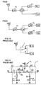
- A high frequency switch shown in Fig. 10 is used for switching connections between a transmission circuit TX and an antenna ANT and between a receiving circuit RX and an antenna ANT via signal lines in a portable digital telephone set, for example.
- An example of a high frequency device, such as a high frequency switch, has a configuration shown in the circuit diagram of Fig. 11. The
high frequency switch 1 is connected to an antenna ANT, a transmission circuit TX and a receiving circuit RX by signal lines V1. A high frequency component, such as a diode D1, has an anode that is connected via a capacitor C1 to the transmission circuit TX. The anode of the diode D1 is also connected to ground via a series circuit including a strip line L1 forming part of a first transmission line and a capacitor C4. The length of the strip line L1 is substantially equal to or less than λ/4, where the wavelength of a signal sent from the transmission circuit TX is λ. A control terminal Vcl is connected to an intermediate point between the strip line L1 and the capacitor C4. A control circuit (not shown) for switching thehigh frequency switch 1 is connected to the control terminal Vcl. A series circuit including a strip line L3 forming part of the first transmission line and a capacitor C6 is connected to both ends of the diode D1 (between the anode and the cathode). The cathode of the diode D1 is connected to the antenna ANT via a capacitor C2. - The receiving circuit RX is connected to the capacitor C2, which is connected to the antenna ANT, via a series circuit including a strip line L2 forming part of the first transmission line and a capacitor C3. As in the case of the strip line L1, the length of the strip line L2 is substantially equal to or less than λ/4. Another high frequency component, for example, a diode D2, has an anode connected to an intermediate point between the strip line L2 and the capacitor C3. The cathode of the diode D2 is connected to ground via a capacitor C5. Further, a control terminal Vc2 is connected to an intermediate point between the diode D2 and the capacitor C5. A control circuit (not shown) for switching the
high frequency switch 1 is connected to the control terminal Vc2 to thereby complete the circuit of thehigh frequency switch 1. - When a signal is transmitted through the
high frequency switch 1, a positive bias voltage is applied to the control terminal Vc1 while a negative bias voltage is applied to the control terminal Vc2. As these voltages work as bias voltages in the forward direction to bias the diodes D1 and D2, the diodes D1 and D2 will be turned ON. At this time, direct currents will be cut by the capacitors C1 to C6 and the voltages applied to the control terminals Vc1 and Vc2 will be applied only on a circuit including the diodes D1 and D2. Thus, the strip line L2 will be grounded by the diode D2 and will resonate at a transmission frequency and impedance will be made almost infinite. Consequently, a signal sent from the transmission circuit TX will be transmitted to the antenna ANT through the capacitor C1, the diode D1 and the capacitor C2 without being transmitted to the side of the receiving circuit RX in most cases. Further, because the strip line L1 is grounded via the capacitor C4, the strip line L1 will resonate at a transmission frequency and impedance will be made almost infinite. As a result, leakage of a transmitted signal to the ground side will be prevented. - On the other hand, at the time of receiving a signal, a negative bias voltage will be applied to the control terminal Vc1 while a positive bias voltage will be applied to the control terminal Vc2. As these voltages work as bias voltages in reverse directions relative to the diodes D1 and D2, the diodes D1 and D2 will be turned OFF, and thereby a signal received from the antenna ANT will be transmitted to the receiving circuit RX through the capacitor C2, the strip line L2 and the capacitor C3 without being transmitted to the transmission circuit TX in most cases.
- In this way, the
high frequency switch 1 allows switching of transmitted and received signals by controlling bias voltages to be applied to the control terminals Vc1 and Vc2. - Further, the series circuit including the strip line L3 and the capacitor C6 are used for increasing impedance on a connection point with the strip line L3 when the diode D1 is OFF and for reducing insertion loss and reflection loss by forming a parallel resonance circuit to be resonated by synthetic capacitance between the capacitor C6 and the diode D1 which is OFF and the inductance component of the strip line L3, and by resonating at its resonance frequency which is substantially the same as a frequency of a received signal.
- Besides the circuit construction of a high frequency switch described above, there are various types of high frequency switches available. For example, a high frequency switch as described in Japanese Laid-Open Patent No. 6-197042 and Japanese Laid-Open Patent No. 6-197043 and a high frequency switch having a circuit configuration such as the one shown in Japanese Laid-Open Patent No. 7-74762 can also be used.
- Further, other high frequency components such as transistors, FETs, and any other suitable device can be used instead of the high frequency components, such as the diodes D1 and D2 described above. In addition, instead of the strip lines L1, L2 and L3, other transmission lines such as coplanar lines and any other suitable components can be used.
- Conventionally, however, problems occur when high frequency devices, such as high frequency switches, are used to form a high frequency apparatus by connecting filters to the high frequency devices. The high frequency devices and filters are designed and manufactured differently and independently and are then connected to each other. As a result, the combined high frequency device and filter occupy relatively large areas on a printed circuit board and make the circuit arrangement thereof more complicated. In addition, impedance matching between the high frequency device and the filter must be done to connect the high frequency device and the filter. Therefore, an impedance matching circuit must be designed specifically for the particular high frequency device and filter to be connected to each other. Once the impedance matching filter is designed, the impedance matching filter must be manufactured and connected to the high frequency device and the filter. Consequently, the cost, time and difficulty of manufacturing an apparatus having an interconnected high frequency device and filter with necessary impedance matching circuit is substantially increased.
- The preferred embodiments of the present invention solve the problems with the conventional apparatus having an interconnected high frequency device and filter. One object of at least one of the preferred embodiments of the present invention is to provide a composite high frequency apparatus having a substantially reduced size for occupying a reduced amount of space on a printed circuit board. Another object of at least one of the preferred embodiments of the present invention is to simplify the circuit arrangement of a composite high frequency apparatus while eliminating the need for an impedance matching circuit.
- In order to solve the problems of the conventional devices described above, the composite high frequency apparatus and method of forming the apparatus according to at least one of the preferred embodiments of the present invention includes a high frequency device mounted on an outer surface of a multilayered base which includes a laminated structure of a plurality of dielectric layers and a signal line connected to a ground electrode, wherein the high frequency device is located at least on the outer surface of the multilayered base or the dielectric layer, a first transmission line connecting the signal line and the ground electrode and a filter connected to the high frequency component via a second transmission line and signal lines located in the multilayer unit.
- Further, a diode is preferably used as a high frequency component, a strip line is preferably used as the transmission line and a high frequency switch is preferably used as the high frequency device. A low-pass filter can be used as the filter. Alternatively, all other suitable high frequency components, transmission lines, high frequency devices and filters can also be used as will be understood from the following description of the preferred embodiments of the present invention.
- By locating the high frequency device and the filter on one multilayered base including a plurality of dielectric layers and thereby creating a composite high frequency apparatus, the overall dimension of the apparatus is reduced as compared to a conventional device wherein a high frequency device and a filter are separately made and then connected to each other. Also, by combining the circuit of the high frequency device and the circuit of the filter and simultaneously forming the high frequency device and the filter, desired impedance matching between the circuit of the high frequency device and the circuit of the filter is achieved without the need for a separate impedance matching circuit.
- Other features and advantages of the present invention will become apparent from the following description of the invention which refers to the accompanying drawings.
-
- Fig. 1 is a diagram showing a circuit of a composite high frequency apparatus according to a preferred embodiment of the present invention;
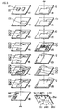
- Fig. 2 is a sectional view showing the composite high frequency apparatus shown in Fig. 1;
- Fig. 3 is an exploded perspective view showing the composite high frequency apparatus of Fig. 1;
- Fig. 4 is a view showing a circuit construction of a composite high frequency apparatus according to another preferred embodiment of the present invention;
- Fig. 5 is a view showing a circuit construction of a composite high frequency apparatus according to another preferred embodiment of the present invention;
- Fig. 6 is a view showing a circuit construction of a composite high frequency apparatus according to another preferred embodiment of the present invention;
- Fig. 7 is a view showing a circuit construction of a composite high frequency apparatus according to another preferred embodiment of the present invention;
- Fig. 8 is a view showing a circuit construction of a composite high frequency apparatus according to another preferred embodiment of the present invention;
- Fig. 9 is a view showing a circuit construction of a composite high frequency apparatus according to another preferred embodiment of the present invention;
- Fig. 10 is a view showing a circuit construction of a conventional high frequency device; and
- Fig. 11 is a diagram showing the circuit of the conventional high frequency device shown in Fig. 10.
- Preferred embodiments of the present invention will be described with reference to the accompanying drawings. Description of elements similar to or the same as the conventional elements shown in Figs. 10 and 11, will be omitted to avoid redundancy. Such similar elements contained in the preferred embodiments of the present invention will be identified by the same reference numerals and characters used to describe the conventional components.
- Fig. 1 is a diagram showing a circuit of a composite high frequency apparatus 2 according to a preferred embodiment of the present invention. In the preferred embodiment shown in Fig. 1, a filter F1 may preferably be a low-pass filter such as a Butterworth type low-pass filter or any other suitable filter.
- The filter F1 is preferably connected between a transmission circuit TX and one end of a capacitor C1 of a
high frequency device 1. The filter F1 preferably includes strip lines L4 and L5 which form a second transmission line. The filter F1 also preferably includes capacitors C7, C8 and C9. Description of the connections relating to the filter F1 is omitted because such connections are known. - Fig. 2 is a sectional view showing the composite high frequency apparatus 2 of Fig. 1. The high frequency apparatus 2 includes a
multilayered base 10. As shown in the preferred embodiment of Fig. 3, themultilayered base 10 is preferably formed by laminatingdielectric layers 11 to 25 of the first to fifteenth dielectric layers successively from top to bottom. Diodes D1 and D2 are preferably mounted on thefirst dielectric layer 11. Capacitor electrodes C51, C11, C21, C31, C12, C22, C32, C13, C33, C61, C15, C35, C63, C41, C71, C81 and C91 are preferably located on thelayers 12 to 15 of the second to the fifth dielectric layers and thelayers 17, 20 and 24 of the seventh, tenth and fourteenth dielectric layers. - Capacitor electrodes C14, C34 and C62 and a strip line electrode L31 are preferably formed on the
sixth dielectric layer 16. Strip line electrodes L41, L51, L11, and L21 are preferably formed on the eighth and twelfthdielectric layers dielectric layers - Further, an external electrode for a transmission circuit TX1, an external electrode for a receiving circuit RX1, an external electrode for an antenna ANT1, external control electrodes Vc11 and Vc22 and external ground electrodes G2 are preferably formed on a lower surface of the fifteenth dielectric layer 25 (25u in Fig. 3). By forming signal line electrodes (not shown in Fig. 3), at desired locations on the
dielectric layers 11 to 25 and by forming external electrodes (not shown in Fig. 3) on the outer surface of themultilayer base 10 and electrically connecting the external electrodes, the composite high frequency apparatus 2 is constructed to have the circuit configuration shown in Fig. 1. - More particularly, capacitor C1 of the
high frequency switch 1 comprises capacitor electrodes C11 to C15, capacitor C2 comprises capacitor electrodes C21 and C22, capacitor C3 comprises capacitor electrodes C31 to C35, capacitor C4 comprises capacitor electrode C41, capacitor C5 comprises capacitor electrode C51, and capacitor C6 comprises capacitor electrodes C61 to C63. Capacitors C7, C8 and C9 of the filter circuit F1 comprise capacitor electrodes C71, C81 and C91, respectively. - Coil patterns L1 to L3 of the
high frequency switch 1 comprise strip line electrodes L11 to L31, respectively. Coil patterns L4 and L5 of the filter circuit F1 comprise strip line electrodes L41 and L51, respectively. - When manufacturing such a composite high frequency apparatus 2, dielectric ceramic green sheets are preferably prepared. On the dielectric ceramic green sheets, electrode paste is preferably printed in accordance with the forms of the respective electrodes and signal lines. Then, by laminating the dielectric ceramic green sheets with electrode paste printed thereon and baking the ceramic green sheets, a multilayered base having laminated dielectric layers will be formed. Further, by printing the electrode paste on the outer surface of the multilayered base and baking the electrode paste, external electrodes will be formed. It is also possible to form the composite high frequency apparatus by printing electrode paste to form external electrodes and baking the electrodes integrally after the dielectric green sheets are laminated.
- The composite high frequency apparatus including a high frequency device and a filter formed on one multilayered base by laminating a plurality of dielectric layers has an overall physical dimension that is substantially less than the conventional devices in which a high frequency device and a filter are separately formed and then connected. The composite high frequency apparatus according to at least one of the preferred embodiments of the present invention achieves a reduced volume and occupies less area on a printed circuit board. Also, by combining the circuit of the high frequency device and the circuit of the filter and simultaneously designing and forming the circuits of the high frequency device and the filter, impedance matching between the circuit of the high frequency device and the circuit of the filter is achieved. Consequently, it is not necessary to design, manufacture and connect an impedance matching circuit between the circuit of the high frequency device and the circuit of the filter. Therefore, the manufacturing and assembly of the circuit of the high frequency device and the circuit of the filter is easier and less expensive than the conventional methods. Further, because the impedance matching circuit is not necessary, the composite high frequency device will be formed in a substantially shorter period of time because the time required for designing and forming the impedance matching circuit is unnecessary.
- Further, in the description of the preferred embodiment of Fig. 1, reference was made to the capacitors and strip lines formed on the multilayered base. However, resistance components like chip resistors, printed resistors, and other suitable resistance components and electronic components may be formed on the surface of the multilayered base or may be formed within the multilayered base.
- In the preferred embodiment of Fig. 1, the high frequency device and the filter are connected such that the filter F1 is connected between the transmission circuit TX and the
high frequency switch 1. However, it is possible to obtain the same effect by selectively connecting the filter F1 between the transmission circuit TX, the receiving circuit RX or the antenna ANT and thehigh frequency switch 1. - Several alternative preferred embodiments of the present invention will be described in the following paragraphs in relation to Figs. 4-9.
- The filter F1 may preferably be connected between the antenna ANT and the
high frequency switch 1 as shown in Fig. 4. - The filter F1 may preferably be connected between the receiving circuit RX and the
high frequency switch 1 as shown in Fig. 5. - The filter F1 may preferably be connected between the transmission circuit TX and the
high frequency switch 1 and between the antenna ANT and thehigh frequency switch 1 as shown in Fig. 6. - The filter F1 may preferably be connected between the transmission circuit TX and the
high frequency switch 1 and between the receiving circuit RX and thehigh frequency switch 1 as shown in Fig. 7. - The filter F1 may preferably be connected between the receiving circuit RX and the
high frequency switch 1 and between the antenna ANT and thehigh frequency switch 1 as shown in Fig. 8. - The filter F1 may preferably be connected between the transmission circuit TX and the
high frequency switch 1, between the receiving circuit RX and thehigh frequency switch 1 and between the antenna ANT and thehigh frequency switch 1 as shown in Fig. 9. - Further, in another preferred embodiment of the present invention, a filter, for example, a low-pass filter, may be connected to the high frequency device. However, instead of a low-pass filter, a high-pass filter, a band-pass filter, a band elimination filter and any other suitable filter may be used to be combined with or connected to the high frequency device.
- The effect of formation according to at least one of the preferred embodiments of the present invention will be described in detail with respect to an example where a low-pass filter is used.
- A composite high frequency apparatus may be constructed by forming a high frequency device such as a high frequency switch including a multilayered base of laminated dielectric layers having the dimensions of about 6.3 x 5.0 x 3.0 mm and a low-pass filter having the dimensions of about 4.5 x 3.2 x 2.0 mm on one multilayered base. As a result, the entire dimensions of the apparatus is about 6.3 x 5.0 x 3.0 mm which are about the same as the entire dimensions of a conventional high frequency switch. The volumes and occupied areas on a printed circuit board of the composite high frequency apparatus produced by at least one preferred embodiment of the present invention are substantially reduced. Further, by combining the circuit of the high frequency device and the circuit of the filter and simultaneously designing and forming the circuits, no impedance matching circuit is needed as with a conventional high frequency device and low-pass filter.
- Thus, according to at least one of the preferred embodiments of the present invention, by creating a composite high frequency apparatus by forming a high frequency device and a filter on one multilayered base made of a plurality of dielectric layers, an overall dimension of the apparatus is substantially less than the overall dimension of the conventional high frequency device and filter which are independently designed and formed and then connected. The composite high frequency apparatus according to at least one of the preferred embodiments of the present invention has reduced volume and occupies substantially less area on a printed circuit board. Further, by combining the circuit of the filter and the circuit of the high frequency device and simultaneously designing and forming the circuits, it is possible to achieve impedance matching between the two circuits. Accordingly, it is not necessary to add an impedance matching circuit and the circuit construction of the preferred embodiments is simplified. In addition, the period of time required for designing, forming and connecting the impedance matching circuit as required in the prior art devices is eliminated because an impedance matching circuit is not necessary in the preferred embodiments of the present invention.
- Although the present invention has been described in relation to particular preferred embodiments thereof, many other variations and modifications and other uses will become apparent to those skilled in the art. It is preferred, therefore, that the present invention be limited not by the specific disclosure herein, but only by the appended claims.
Claims (20)
- A composite high frequency apparatus comprising:
a single multilayered unit (2) including at least one high frequency device (1) and a high frequency filter (F1) being electrically connected to each other within said single multilayered unit. - The composite high frequency apparatus of claim 1, wherein the at least one high frequency device (1) comprises a high frequency switch.
- The composite high frequency apparatus of claim 1, wherein the high frequency filter (F1) comprises at least one of a low-pass filter, a band-pass filter, a band elimination filter and a high-pass filter.
- The composite high frequency apparatus of claim 1, wherein the single multilayered unit (2) includes a high frequency component (D1/D2) mounted on an outer surface of the multilayered base (10).
- The composite high frequency apparatus of claim 4, wherein the high frequency component comprises at least one of a diode (D1/D2), a transistor and a FET.
- The composite high frequency apparatus of claim 1, wherein the single multilayered unit (2) comprises a plurality of laminated dielectric layers (11-25).
- The composite high frequency apparatus of claim 6, wherein the high frequency device (1) is located on at least one of the outer surfaces of one of the dielectric layers of the single multilayered unit (2).
- The composite high frequency apparatus of claim 5, wherein the single multilayered unit (2) further comprises a signal line connected to a ground electrode, a first transmission line (L1/L11) connected between the signal line and the ground electrode.
- The composite high frequency apparatus of claim 1, wherein the high frequency filter (F1) is connected with a high frequency switch (1) by a second transmission line (L2/L21) and signal lines located in the single multilayered unit (2).
- The composite high frequency apparatus of claim 9, wherein the single multilayered unit (2) further comprises a signal line connected to a ground electrode, the second transmission line is connected to the high frequency device by the signal line.
- A method of forming a composite high frequency apparatus, the method comprising steps of:
forming a plurality of dielectric layers (11-25) including a plurality of electronic components formed thereon;
joining the plurality of dielectric layers to connect the plurality of electronic components and to form a single multilayered unit (2) including at least one high frequency device (1) and a high frequency filter (F1) being electrically connected to each other within said single multilayered unit. - The method of claim 11, wherein the step of forming the plurality of dielectric layers (11-25) includes the step of forming a plurality of dielectric ceramic green sheets.
- The method of claim 11, wherein the step of forming the plurality of dielectric layers (11-25) includes the step of forming a plurality of electronic components by printing electrode paste on the plurality of dielectric layers.
- The method of claim 13, further comprising the steps of laminating the dielectric layers having the electronic components printed thereon and baking the dielectric layers and electronic components.
- The method of claim 14, further comprising the step of forming external electrodes on at least one exterior surface (25u) of the single multilayer unit (2) and baking the external electrodes.
- A method of forming a composite high frequency apparatus, the method comprising the step of:
simultaneously forming a high frequency device (1) and a high frequency filter (F1) in a single unit (2), wherein the high frequency device and the high frequency filter are electrically connected to each other and an impedance of the high frequency device (1) is substantially equal to an impedance of the high frequency filter (F1). - The method of claim 16, wherein said high frequency device (1) comprises a high frequency switch.
- The method of claim 16, wherein said high frequency filter (F1) comprises one of a low-pass filter, a band-pass filter, a band elimination filter and a high-pass filter.
- The method of claim 16, wherein the step of simultaneously forming the high frequency device (1) and the high frequency filter (F1) includes the step of forming a single multilayered unit (2) including a plurality of dielectric layers (11-25) having a plurality of electronic components formed thereon.
- The method of claim 19, further comprising the step of joining the plurality of dielectric layers (11- 25) to connect the plurality of electronic components.
Priority Applications (6)
| Application Number | Priority Date | Filing Date | Title |
|---|---|---|---|
| EP03005265A EP1331687B1 (en) | 1994-09-28 | 1995-09-28 | Composite high frequency apparatus |
| EP01100589A EP1113520B1 (en) | 1994-09-28 | 1995-09-28 | Composite high frequency apparatus |
| EP01100590A EP1113521A1 (en) | 1994-09-28 | 1995-09-28 | Method of forming a composite high frequency apparatus |
| EP01103863A EP1111708B1 (en) | 1994-09-28 | 1995-09-28 | Composite high frequency apparatus and method of forming same |
| EP02005653A EP1215748B1 (en) | 1994-09-28 | 1995-09-28 | Composite high frequency apparatus |
| EP01100588A EP1113519B1 (en) | 1994-09-28 | 1995-09-28 | Composite high frequency apparatus |
Applications Claiming Priority (3)
| Application Number | Priority Date | Filing Date | Title |
|---|---|---|---|
| JP6233204A JP3031178B2 (en) | 1994-09-28 | 1994-09-28 | Composite high frequency components |
| JP23320494 | 1994-09-28 | ||
| JP233204/94 | 1994-09-28 |
Related Child Applications (4)
| Application Number | Title | Priority Date | Filing Date |
|---|---|---|---|
| EP01100589A Division EP1113520B1 (en) | 1994-09-28 | 1995-09-28 | Composite high frequency apparatus |
| EP01100590A Division EP1113521A1 (en) | 1994-09-28 | 1995-09-28 | Method of forming a composite high frequency apparatus |
| EP01103863A Division EP1111708B1 (en) | 1994-09-28 | 1995-09-28 | Composite high frequency apparatus and method of forming same |
| EP01100588A Division EP1113519B1 (en) | 1994-09-28 | 1995-09-28 | Composite high frequency apparatus |
Publications (2)
| Publication Number | Publication Date |
|---|---|
| EP0704925A1 true EP0704925A1 (en) | 1996-04-03 |
| EP0704925B1 EP0704925B1 (en) | 2001-07-25 |
Family
ID=16951389
Family Applications (8)
| Application Number | Title | Priority Date | Filing Date |
|---|---|---|---|
| EP95402177A Revoked EP0704925B1 (en) | 1994-09-28 | 1995-09-28 | Composite high frequency apparatus and method for forming same |
| EP01100589A Revoked EP1113520B1 (en) | 1994-09-28 | 1995-09-28 | Composite high frequency apparatus |
| EP03022629A Ceased EP1378958A1 (en) | 1994-09-28 | 1995-09-28 | Composite high frequency apparatus |
| EP02005653A Revoked EP1215748B1 (en) | 1994-09-28 | 1995-09-28 | Composite high frequency apparatus |
| EP01100588A Revoked EP1113519B1 (en) | 1994-09-28 | 1995-09-28 | Composite high frequency apparatus |
| EP01100590A Withdrawn EP1113521A1 (en) | 1994-09-28 | 1995-09-28 | Method of forming a composite high frequency apparatus |
| EP03005265A Revoked EP1331687B1 (en) | 1994-09-28 | 1995-09-28 | Composite high frequency apparatus |
| EP01103863A Revoked EP1111708B1 (en) | 1994-09-28 | 1995-09-28 | Composite high frequency apparatus and method of forming same |
Family Applications After (7)
| Application Number | Title | Priority Date | Filing Date |
|---|---|---|---|
| EP01100589A Revoked EP1113520B1 (en) | 1994-09-28 | 1995-09-28 | Composite high frequency apparatus |
| EP03022629A Ceased EP1378958A1 (en) | 1994-09-28 | 1995-09-28 | Composite high frequency apparatus |
| EP02005653A Revoked EP1215748B1 (en) | 1994-09-28 | 1995-09-28 | Composite high frequency apparatus |
| EP01100588A Revoked EP1113519B1 (en) | 1994-09-28 | 1995-09-28 | Composite high frequency apparatus |
| EP01100590A Withdrawn EP1113521A1 (en) | 1994-09-28 | 1995-09-28 | Method of forming a composite high frequency apparatus |
| EP03005265A Revoked EP1331687B1 (en) | 1994-09-28 | 1995-09-28 | Composite high frequency apparatus |
| EP01103863A Revoked EP1111708B1 (en) | 1994-09-28 | 1995-09-28 | Composite high frequency apparatus and method of forming same |
Country Status (5)
| Country | Link |
|---|---|
| US (2) | US5783976A (en) |
| EP (8) | EP0704925B1 (en) |
| JP (1) | JP3031178B2 (en) |
| DE (7) | DE69521860T2 (en) |
| HK (1) | HK1044417B (en) |
Cited By (18)
| Publication number | Priority date | Publication date | Assignee | Title |
|---|---|---|---|---|
| EP0837516A2 (en) * | 1996-10-21 | 1998-04-22 | Murata Manufacturing Co., Ltd. | High-frequency composite part |
| EP0920128A2 (en) | 1997-11-26 | 1999-06-02 | Murata Manufacturing Co., Ltd. | Impedance stabilizing unit and high-frequency module using the unit |
| EP0921642A2 (en) * | 1997-12-03 | 1999-06-09 | Hitachi Metals, Ltd. | Multiband high-frequency switching module |
| WO2000003450A1 (en) * | 1998-07-09 | 2000-01-20 | Motorola, Inc. | Multilayer ceramic integrated circuit including receiver front-end |
| EP0998035A2 (en) * | 1998-10-27 | 2000-05-03 | Murata Manufacturing Co., Ltd. | Composite high frequency component and mobile communication device including the same |
| EP1024605A2 (en) * | 1999-01-27 | 2000-08-02 | Murata Manufacturing Co., Ltd. | High-frequency switch |
| EP0820155A3 (en) * | 1996-07-17 | 2001-02-07 | Murata Manufacturing Co., Ltd. | Duplexer |
| FR2797740A1 (en) * | 1999-08-19 | 2001-02-23 | Sony Corp | CIRCUIT BOARD, SEMICONDUCTOR COMPONENT AND METHOD OF MANUFACTURING IT |
| EP1126624A2 (en) * | 2000-01-21 | 2001-08-22 | Murata Manufacturing Co., Ltd. | High-frequency switch |
| EP1220316A2 (en) * | 2000-12-28 | 2002-07-03 | Matsushita Electric Industrial Co., Ltd. | High-frequency switching module and high-frequency apparatus equipped with the same |
| DE10201438A1 (en) * | 2002-01-16 | 2003-07-24 | Epcos Ag | Antenna switching circuit for mobile telephone has antenna input and control line of switching module coupled to respective electrostatic discharge protection devices |
| DE10201433A1 (en) * | 2002-01-16 | 2003-07-24 | Epcos Ag | Antenna switching circuit for mobile telephone has antenna input coupled to electrostatic discharge protection device |
| DE10201434A1 (en) * | 2002-01-16 | 2004-03-04 | Epcos Ag | Antenna switching circuit for mobile telephone has antenna input coupled to electrostatic discharge protection device |
| US6862436B2 (en) | 2001-02-27 | 2005-03-01 | Ngk Spark Plug Co., Ltd. | High frequency circuit board and antenna switch module for high frequency using the same |
| US6937845B2 (en) | 2000-03-31 | 2005-08-30 | Murata Manufacturing Co., Ltd. | High-frequency module and radio device using the same |
| US7343137B2 (en) | 2001-09-28 | 2008-03-11 | Epcos Ag | Circuit, switching module comprising the same, and use of said switching module |
| US7492565B2 (en) | 2001-09-28 | 2009-02-17 | Epcos Ag | Bandpass filter electrostatic discharge protection device |
| US8014731B2 (en) | 2001-01-18 | 2011-09-06 | Epcos Ag | Electric circuit module, circuit module arrangement and use of said circuit module and of said circuit module arrangement |
Families Citing this family (37)
| Publication number | Priority date | Publication date | Assignee | Title |
|---|---|---|---|---|
| US5999065A (en) * | 1995-08-24 | 1999-12-07 | Murata Manufacturing Co., Ltd. | Composite high-frequency component |
| KR100677005B1 (en) * | 1996-10-31 | 2007-01-31 | 라미나 세라믹스, 인크. | Integrated electronic circuit |
| JP3394401B2 (en) * | 1996-11-22 | 2003-04-07 | ティーディーケイ株式会社 | Low-pass filter |
| JPH10200360A (en) * | 1997-01-07 | 1998-07-31 | Tdk Corp | Laminated balun transformer |
| FI971850A (en) * | 1997-04-30 | 1998-10-31 | Nokia Telecommunications Oy | Arrangements for reducing interference between radio frequency signals |
| JPH11112264A (en) * | 1997-10-08 | 1999-04-23 | Murata Mfg Co Ltd | Filter |
| US5929729A (en) * | 1997-10-24 | 1999-07-27 | Com Dev Limited | Printed lumped element stripline circuit ground-signal-ground structure |
| JP2000049651A (en) * | 1998-07-27 | 2000-02-18 | Hitachi Metals Ltd | High frequency switch module for multi-band |
| JPH11205066A (en) * | 1998-01-13 | 1999-07-30 | Murata Mfg Co Ltd | Filter |
| JP3255105B2 (en) * | 1998-01-22 | 2002-02-12 | 株式会社村田製作所 | High frequency composite parts |
| JP3304898B2 (en) * | 1998-11-20 | 2002-07-22 | 株式会社村田製作所 | Composite high frequency component and mobile communication device using the same |
| JP2000307452A (en) * | 1999-02-16 | 2000-11-02 | Murata Mfg Co Ltd | High-frequency composite component and portable radio equipment using same |
| US6731184B1 (en) | 1999-07-29 | 2004-05-04 | Murata Manufacturing Co., Ltd. | High frequency switching component |
| JP2001136045A (en) * | 1999-08-23 | 2001-05-18 | Murata Mfg Co Ltd | Layered composite electronic component |
| JP2001267957A (en) * | 2000-03-15 | 2001-09-28 | Ngk Insulators Ltd | Transmitter-receiver |
| JP4596300B2 (en) * | 2000-06-09 | 2010-12-08 | 日立金属株式会社 | High frequency switch module |
| JP3711846B2 (en) * | 2000-07-27 | 2005-11-02 | 株式会社村田製作所 | High frequency module and mobile communication device using the same |
| US6600385B2 (en) | 2000-08-21 | 2003-07-29 | Tdk Corporation | Front end module for mobile communications apparatus |
| JP3800504B2 (en) | 2001-05-15 | 2006-07-26 | Tdk株式会社 | Front-end module |
| JP3772771B2 (en) | 2001-05-18 | 2006-05-10 | 松下電器産業株式会社 | Multiband high frequency switch |
| JP2003032001A (en) * | 2001-07-13 | 2003-01-31 | Murata Mfg Co Ltd | Compound high frequency switch, high frequency module and communication device |
| US20050059371A1 (en) * | 2001-09-28 | 2005-03-17 | Christian Block | Circuit arrangement, switching module comprising said circuit arrangement and use of switching module |
| JP2004104394A (en) | 2002-09-09 | 2004-04-02 | Matsushita Electric Ind Co Ltd | High frequency switch |
| DE10241674A1 (en) | 2002-09-09 | 2004-03-25 | Epcos Ag | Multiple-resonance filter formed as multilayer component, has three or more multilayer capacitors, with outer capacitors having same capacitance |
| DE10246098A1 (en) | 2002-10-02 | 2004-04-22 | Epcos Ag | circuitry |
| JP2004147045A (en) | 2002-10-24 | 2004-05-20 | Matsushita Electric Ind Co Ltd | High-frequency switch |
| US6962078B2 (en) | 2002-12-24 | 2005-11-08 | Lexmark International, Inc. | Liquid level detection gauge and associated methods |
| WO2005014796A2 (en) | 2003-08-08 | 2005-02-17 | Invitrogen Corporation | Methods and compositions for seamless cloning of nucleic acid molecules |
| US7423332B2 (en) * | 2003-08-26 | 2008-09-09 | Delphi Technologies, Inc. | Vertical laminated electrical switch circuit |
| JP2005167468A (en) * | 2003-12-01 | 2005-06-23 | Renesas Technology Corp | Electronic apparatus and semiconductor device |
| ATE469984T1 (en) | 2003-12-01 | 2010-06-15 | Life Technologies Corp | NUCLEIC ACID MOLECULES CONTAINING RECOMBINATION SITE AND METHOD FOR USE THEREOF |
| US7899492B2 (en) * | 2004-07-16 | 2011-03-01 | Sellerbid, Inc. | Methods, systems and apparatus for displaying the multimedia information from wireless communication networks |
| US7084722B2 (en) * | 2004-07-22 | 2006-08-01 | Northrop Grumman Corp. | Switched filterbank and method of making the same |
| EP1876722B1 (en) * | 2005-04-28 | 2016-08-24 | Murata Manufacturing Co., Ltd. | High frequency switching module and method for adjusting frequency characteristic of high frequency circuit |
| US7423498B2 (en) * | 2005-09-20 | 2008-09-09 | Raytheon Company | Compact multilayer circuit |
| CN101401304B (en) * | 2006-08-21 | 2011-04-13 | 株式会社村田制作所 | High frequency module |
| CN111371431B (en) * | 2020-03-20 | 2023-03-14 | 上海航天电子通讯设备研究所 | Three-dimensional packaged multilayer stacked structure switch filter bank |
Citations (10)
| Publication number | Priority date | Publication date | Assignee | Title |
|---|---|---|---|---|
| US2473293A (en) | 1945-10-23 | 1949-06-14 | Lorentzen Hardware Mfg Corp | Venetian blind bracket |
| US4353132A (en) * | 1980-01-28 | 1982-10-05 | Hitachi, Ltd. | Double superheterodyne tuner |
| US4899118A (en) * | 1988-12-27 | 1990-02-06 | Hughes Aircraft Company | Low temperature cofired ceramic packages for microwave and millimeter wave gallium arsenide integrated circuits |
| EP0468801A2 (en) * | 1990-07-25 | 1992-01-29 | Ngk Insulators, Ltd. | Distributed constant circuit board using ceramic substrate material |
| JPH04301901A (en) | 1991-03-28 | 1992-10-26 | Sanyo Electric Co Ltd | Substrate for high frequency module |
| JPH06197040A (en) | 1992-12-26 | 1994-07-15 | Murata Mfg Co Ltd | High frequency switch |
| JPH06197043A (en) | 1992-12-26 | 1994-07-15 | Murata Mfg Co Ltd | High frequency switch |
| JPH06197042A (en) | 1992-12-26 | 1994-07-15 | Murata Mfg Co Ltd | High frequency switch |
| JPH06204912A (en) | 1992-12-29 | 1994-07-22 | Tdk Corp | Transmission/reception terminal circuit device |
| JPH0774762A (en) | 1993-09-03 | 1995-03-17 | Toshiba Corp | Bus line data controller |
Family Cites Families (7)
| Publication number | Priority date | Publication date | Assignee | Title |
|---|---|---|---|---|
| JPS59135933A (en) * | 1983-01-25 | 1984-08-04 | Matsushita Electric Ind Co Ltd | Antenna switching circuit |
| JPS6014544U (en) | 1983-07-07 | 1985-01-31 | パイオニア株式会社 | antenna switching circuit |
| US5255318A (en) * | 1991-03-22 | 1993-10-19 | North American Philips Corporation | Expandable cable television subscriber control system |
| JPH0514052A (en) | 1991-07-03 | 1993-01-22 | Tdk Corp | High frequency circuit module with filter |
| US5355524A (en) * | 1992-01-21 | 1994-10-11 | Motorola, Inc. | Integrated radio receiver/transmitter structure |
| US5450046A (en) * | 1992-10-29 | 1995-09-12 | Nec Corporation | Composite microwave circuit module assembly and its connection structure |
| DE59402270D1 (en) | 1993-03-25 | 1997-05-07 | Schlatter Ag | Intermittent straightening of wire |
-
1994
- 1994-09-28 JP JP6233204A patent/JP3031178B2/en not_active Expired - Lifetime
-
1995
- 1995-08-24 US US08/518,667 patent/US5783976A/en not_active Expired - Lifetime
- 1995-09-28 EP EP95402177A patent/EP0704925B1/en not_active Revoked
- 1995-09-28 DE DE69521860T patent/DE69521860T2/en not_active Revoked
- 1995-09-28 DE DE69531370T patent/DE69531370T2/en not_active Revoked
- 1995-09-28 EP EP01100589A patent/EP1113520B1/en not_active Revoked
- 1995-09-28 EP EP03022629A patent/EP1378958A1/en not_active Ceased
- 1995-09-28 DE DE69531371T patent/DE69531371T2/en not_active Expired - Lifetime
- 1995-09-28 EP EP02005653A patent/EP1215748B1/en not_active Revoked
- 1995-09-28 EP EP01100588A patent/EP1113519B1/en not_active Revoked
- 1995-09-28 DE DE69532619T patent/DE69532619T2/en not_active Revoked
- 1995-09-28 DE DE1215748T patent/DE1215748T1/en active Pending
- 1995-09-28 DE DE69531375T patent/DE69531375T2/en not_active Revoked
- 1995-09-28 EP EP01100590A patent/EP1113521A1/en not_active Withdrawn
- 1995-09-28 EP EP03005265A patent/EP1331687B1/en not_active Revoked
- 1995-09-28 EP EP01103863A patent/EP1111708B1/en not_active Revoked
- 1995-09-28 DE DE69531368T patent/DE69531368T2/en not_active Revoked
-
1998
- 1998-04-30 US US09/070,319 patent/US5990732A/en not_active Expired - Lifetime
-
2002
- 2002-07-03 HK HK02104984.8A patent/HK1044417B/en not_active IP Right Cessation
Patent Citations (10)
| Publication number | Priority date | Publication date | Assignee | Title |
|---|---|---|---|---|
| US2473293A (en) | 1945-10-23 | 1949-06-14 | Lorentzen Hardware Mfg Corp | Venetian blind bracket |
| US4353132A (en) * | 1980-01-28 | 1982-10-05 | Hitachi, Ltd. | Double superheterodyne tuner |
| US4899118A (en) * | 1988-12-27 | 1990-02-06 | Hughes Aircraft Company | Low temperature cofired ceramic packages for microwave and millimeter wave gallium arsenide integrated circuits |
| EP0468801A2 (en) * | 1990-07-25 | 1992-01-29 | Ngk Insulators, Ltd. | Distributed constant circuit board using ceramic substrate material |
| JPH04301901A (en) | 1991-03-28 | 1992-10-26 | Sanyo Electric Co Ltd | Substrate for high frequency module |
| JPH06197040A (en) | 1992-12-26 | 1994-07-15 | Murata Mfg Co Ltd | High frequency switch |
| JPH06197043A (en) | 1992-12-26 | 1994-07-15 | Murata Mfg Co Ltd | High frequency switch |
| JPH06197042A (en) | 1992-12-26 | 1994-07-15 | Murata Mfg Co Ltd | High frequency switch |
| JPH06204912A (en) | 1992-12-29 | 1994-07-22 | Tdk Corp | Transmission/reception terminal circuit device |
| JPH0774762A (en) | 1993-09-03 | 1995-03-17 | Toshiba Corp | Bus line data controller |
Non-Patent Citations (4)
| Title |
|---|
| PATENT ABSTRACTS OF JAPAN vol. 017, no. 125 (E - 1332) 16 March 1993 (1993-03-16) |
| PATENT ABSTRACTS OF JAPAN vol. 018, no. 549 (E - 1618) 19 October 1994 (1994-10-19) |
| PATENT ABSTRACTS OF JAPAN vol. 018, no. 560 (E - 1621) 26 October 1994 (1994-10-26) |
| Y. TAGUCHI ET AL.: "Microwave characteristics of alumina-glass composite multi-layer substrates with co-fired copper conductors", IEICE TRANSACTIONS ON ELECTRONICS, vol. E76-c, no. 6, TOKYO JP, pages 912 - 918, XP000389645 * |
Cited By (39)
| Publication number | Priority date | Publication date | Assignee | Title |
|---|---|---|---|---|
| EP0820155A3 (en) * | 1996-07-17 | 2001-02-07 | Murata Manufacturing Co., Ltd. | Duplexer |
| EP1381108A3 (en) * | 1996-10-21 | 2004-12-29 | Murata Manufacturing Co., Ltd. | High-frequency switch |
| EP1381108A2 (en) * | 1996-10-21 | 2004-01-14 | Murata Manufacturing Co., Ltd. | High-frequency switch |
| EP0837516A2 (en) * | 1996-10-21 | 1998-04-22 | Murata Manufacturing Co., Ltd. | High-frequency composite part |
| EP0837516A3 (en) * | 1996-10-21 | 2000-05-17 | Murata Manufacturing Co., Ltd. | High-frequency composite part |
| EP0920128A2 (en) | 1997-11-26 | 1999-06-02 | Murata Manufacturing Co., Ltd. | Impedance stabilizing unit and high-frequency module using the unit |
| EP1418679A1 (en) * | 1997-12-03 | 2004-05-12 | Hitachi Metals, Ltd. | Multiband high-frequency switching module |
| EP1443666A3 (en) * | 1997-12-03 | 2004-09-01 | Hitachi Metals, Ltd. | Multiband high-frequency switching module |
| EP0921642A3 (en) * | 1997-12-03 | 2001-11-14 | Hitachi Metals, Ltd. | Multiband high-frequency switching module |
| EP1443666A2 (en) * | 1997-12-03 | 2004-08-04 | Hitachi Metals, Ltd. | Multiband high-frequency switching module |
| EP0921642A2 (en) * | 1997-12-03 | 1999-06-09 | Hitachi Metals, Ltd. | Multiband high-frequency switching module |
| WO2000003450A1 (en) * | 1998-07-09 | 2000-01-20 | Motorola, Inc. | Multilayer ceramic integrated circuit including receiver front-end |
| EP0998035A2 (en) * | 1998-10-27 | 2000-05-03 | Murata Manufacturing Co., Ltd. | Composite high frequency component and mobile communication device including the same |
| US7200365B2 (en) | 1998-10-27 | 2007-04-03 | Murata Manufacturing Co., Ltd. | Composite high frequency component and mobile communication device including the same |
| EP1650865A3 (en) * | 1998-10-27 | 2006-10-25 | Murata Manufacturing Co., Ltd. | Composite high frequency component and mobile communication device including the same |
| EP0998035A3 (en) * | 1998-10-27 | 2003-11-05 | Murata Manufacturing Co., Ltd. | Composite high frequency component and mobile communication device including the same |
| EP1583253A3 (en) * | 1999-01-27 | 2005-10-26 | Murata Manufacturing Co., Ltd. | High-frequency switch |
| EP1024605A3 (en) * | 1999-01-27 | 2003-12-03 | Murata Manufacturing Co., Ltd. | High-frequency switch |
| US6897738B2 (en) | 1999-01-27 | 2005-05-24 | Murata Manufacturing Co., Ltd. | High-frequency switch |
| EP1583253A2 (en) * | 1999-01-27 | 2005-10-05 | Murata Manufacturing Co., Ltd. | High-frequency switch |
| US7391284B2 (en) | 1999-01-27 | 2008-06-24 | Murata Manufacturing Co., Ltd. | High-frequency switch |
| EP1024605A2 (en) * | 1999-01-27 | 2000-08-02 | Murata Manufacturing Co., Ltd. | High-frequency switch |
| FR2797740A1 (en) * | 1999-08-19 | 2001-02-23 | Sony Corp | CIRCUIT BOARD, SEMICONDUCTOR COMPONENT AND METHOD OF MANUFACTURING IT |
| EP1126624A3 (en) * | 2000-01-21 | 2003-01-02 | Murata Manufacturing Co., Ltd. | High-frequency switch |
| EP1126624A2 (en) * | 2000-01-21 | 2001-08-22 | Murata Manufacturing Co., Ltd. | High-frequency switch |
| US6937845B2 (en) | 2000-03-31 | 2005-08-30 | Murata Manufacturing Co., Ltd. | High-frequency module and radio device using the same |
| EP1220316A2 (en) * | 2000-12-28 | 2002-07-03 | Matsushita Electric Industrial Co., Ltd. | High-frequency switching module and high-frequency apparatus equipped with the same |
| US6831528B2 (en) | 2000-12-28 | 2004-12-14 | Matsushita Electric Industrial Co., Ltd. | High-frequency switching module and high-frequency apparatus equipped with the same |
| EP1220316A3 (en) * | 2000-12-28 | 2004-06-23 | Matsushita Electric Industrial Co., Ltd. | High-frequency switching module and high-frequency apparatus equipped with the same |
| CN1300939C (en) * | 2000-12-28 | 2007-02-14 | 松下电器产业株式会社 | High-frequency switch assembly and high-frequency instrument mounting said high-frequency switch assembly |
| EP1892760A3 (en) * | 2000-12-28 | 2008-05-28 | Matsushita Electric Industrial Co., Ltd. | High-frequency switching module and high-frequency apparatus equipped with the same |
| US8014731B2 (en) | 2001-01-18 | 2011-09-06 | Epcos Ag | Electric circuit module, circuit module arrangement and use of said circuit module and of said circuit module arrangement |
| US6862436B2 (en) | 2001-02-27 | 2005-03-01 | Ngk Spark Plug Co., Ltd. | High frequency circuit board and antenna switch module for high frequency using the same |
| US7492565B2 (en) | 2001-09-28 | 2009-02-17 | Epcos Ag | Bandpass filter electrostatic discharge protection device |
| US7343137B2 (en) | 2001-09-28 | 2008-03-11 | Epcos Ag | Circuit, switching module comprising the same, and use of said switching module |
| DE10201434A1 (en) * | 2002-01-16 | 2004-03-04 | Epcos Ag | Antenna switching circuit for mobile telephone has antenna input coupled to electrostatic discharge protection device |
| DE10201438A1 (en) * | 2002-01-16 | 2003-07-24 | Epcos Ag | Antenna switching circuit for mobile telephone has antenna input and control line of switching module coupled to respective electrostatic discharge protection devices |
| DE10201433B4 (en) * | 2002-01-16 | 2010-04-15 | Epcos Ag | Circuit arrangement, switching module with the circuit arrangement and use of the switching module |
| DE10201433A1 (en) * | 2002-01-16 | 2003-07-24 | Epcos Ag | Antenna switching circuit for mobile telephone has antenna input coupled to electrostatic discharge protection device |
Also Published As
| Publication number | Publication date |
|---|---|
| US5990732A (en) | 1999-11-23 |
| EP1113520B1 (en) | 2003-07-23 |
| EP1215748A1 (en) | 2002-06-19 |
| EP1215748B1 (en) | 2003-07-23 |
| EP1113520A1 (en) | 2001-07-04 |
| DE69531368T2 (en) | 2004-04-15 |
| DE69532619T2 (en) | 2004-07-29 |
| EP1378958A1 (en) | 2004-01-07 |
| JPH0897743A (en) | 1996-04-12 |
| EP1113519B1 (en) | 2003-07-23 |
| US5783976A (en) | 1998-07-21 |
| HK1044417A1 (en) | 2002-10-18 |
| DE69532619D1 (en) | 2004-04-01 |
| DE69531370D1 (en) | 2003-08-28 |
| EP1111708A1 (en) | 2001-06-27 |
| DE1215748T1 (en) | 2002-11-28 |
| EP0704925B1 (en) | 2001-07-25 |
| DE69531371T2 (en) | 2004-04-15 |
| HK1044417B (en) | 2004-03-05 |
| DE69521860T2 (en) | 2002-04-11 |
| DE69531375D1 (en) | 2003-08-28 |
| DE69531370T2 (en) | 2004-04-15 |
| JP3031178B2 (en) | 2000-04-10 |
| DE69531368D1 (en) | 2003-08-28 |
| DE69531371D1 (en) | 2003-08-28 |
| EP1331687A1 (en) | 2003-07-30 |
| EP1113521A1 (en) | 2001-07-04 |
| EP1111708B1 (en) | 2003-07-23 |
| EP1113519A1 (en) | 2001-07-04 |
| DE69531375T2 (en) | 2004-04-15 |
| DE69521860D1 (en) | 2001-08-30 |
| EP1331687B1 (en) | 2004-02-25 |
Similar Documents
| Publication | Publication Date | Title |
|---|---|---|
| US5783976A (en) | Composite high frequency apparatus and method of forming same | |
| KR100261751B1 (en) | Composite high frequency component | |
| US6788958B2 (en) | High-frequency module and mobile communication apparatus using the same | |
| US6060960A (en) | Duplexer comprising a SAW filter disposed on a multi-layer substrate | |
| US5473293A (en) | High-frequency switch | |
| EP1024605A2 (en) | High-frequency switch | |
| US5999065A (en) | Composite high-frequency component | |
| JP3191213B2 (en) | High frequency switch module | |
| JP3887805B2 (en) | Diode switch | |
| JP4114106B2 (en) | Composite switch circuit and composite switch circuit component | |
| JPH10276117A (en) | Composite switch circuit parts | |
| JPH10135704A (en) | Diode switch | |
| JPH10135702A (en) | Diode switch | |
| JP2005073096A (en) | Composite high frequency component | |
| JPH10276002A (en) | Diode switch | |
| JP2007325301A (en) | Composite switch circuit and composite switch circuit component |
Legal Events
| Date | Code | Title | Description |
|---|---|---|---|
| PUAI | Public reference made under article 153(3) epc to a published international application that has entered the european phase |
Free format text: ORIGINAL CODE: 0009012 |
|
| AK | Designated contracting states |
Kind code of ref document: A1 Designated state(s): DE FR GB |
|
| 17P | Request for examination filed |
Effective date: 19960918 |
|
| 17Q | First examination report despatched |
Effective date: 19990622 |
|
| GRAG | Despatch of communication of intention to grant |
Free format text: ORIGINAL CODE: EPIDOS AGRA |
|
| GRAG | Despatch of communication of intention to grant |
Free format text: ORIGINAL CODE: EPIDOS AGRA |
|
| GRAG | Despatch of communication of intention to grant |
Free format text: ORIGINAL CODE: EPIDOS AGRA |
|
| GRAH | Despatch of communication of intention to grant a patent |
Free format text: ORIGINAL CODE: EPIDOS IGRA |
|
| GRAH | Despatch of communication of intention to grant a patent |
Free format text: ORIGINAL CODE: EPIDOS IGRA |
|
| TPAD | Observations filed by third parties |
Free format text: ORIGINAL CODE: EPIDOS TIPA |
|
| GRAA | (expected) grant |
Free format text: ORIGINAL CODE: 0009210 |
|
| TPAD | Observations filed by third parties |
Free format text: ORIGINAL CODE: EPIDOS TIPA |
|
| AK | Designated contracting states |
Kind code of ref document: B1 Designated state(s): DE FR GB |
|
| REF | Corresponds to: |
Ref document number: 69521860 Country of ref document: DE Date of ref document: 20010830 |
|
| ET | Fr: translation filed | ||
| REG | Reference to a national code |
Ref country code: GB Ref legal event code: IF02 |
|
| PLBQ | Unpublished change to opponent data |
Free format text: ORIGINAL CODE: EPIDOS OPPO |
|
| PLBI | Opposition filed |
Free format text: ORIGINAL CODE: 0009260 |
|
| PLBQ | Unpublished change to opponent data |
Free format text: ORIGINAL CODE: EPIDOS OPPO |
|
| PLBI | Opposition filed |
Free format text: ORIGINAL CODE: 0009260 |
|
| PLBF | Reply of patent proprietor to notice(s) of opposition |
Free format text: ORIGINAL CODE: EPIDOS OBSO |
|
| 26 | Opposition filed |
Opponent name: DAVID CLARK Effective date: 20020418 |
|
| 26 | Opposition filed |
Opponent name: EPCOS AG Effective date: 20020425 Opponent name: DAVID CLARK Effective date: 20020418 |
|
| PLBF | Reply of patent proprietor to notice(s) of opposition |
Free format text: ORIGINAL CODE: EPIDOS OBSO |
|
| PLBF | Reply of patent proprietor to notice(s) of opposition |
Free format text: ORIGINAL CODE: EPIDOS OBSO |
|
| RDAF | Communication despatched that patent is revoked |
Free format text: ORIGINAL CODE: EPIDOSNREV1 |
|
| APBP | Date of receipt of notice of appeal recorded |
Free format text: ORIGINAL CODE: EPIDOSNNOA2O |
|
| APBM | Appeal reference recorded |
Free format text: ORIGINAL CODE: EPIDOSNREFNO |
|
| APBQ | Date of receipt of statement of grounds of appeal recorded |
Free format text: ORIGINAL CODE: EPIDOSNNOA3O |
|
| APAH | Appeal reference modified |
Free format text: ORIGINAL CODE: EPIDOSCREFNO |
|
| APAH | Appeal reference modified |
Free format text: ORIGINAL CODE: EPIDOSCREFNO |
|
| PGFP | Annual fee paid to national office [announced via postgrant information from national office to epo] |
Ref country code: FR Payment date: 20060908 Year of fee payment: 12 |
|
| PGFP | Annual fee paid to national office [announced via postgrant information from national office to epo] |
Ref country code: DE Payment date: 20060922 Year of fee payment: 12 |
|
| PGFP | Annual fee paid to national office [announced via postgrant information from national office to epo] |
Ref country code: GB Payment date: 20060927 Year of fee payment: 12 |
|
| APBU | Appeal procedure closed |
Free format text: ORIGINAL CODE: EPIDOSNNOA9O |
|
| RDAG | Patent revoked |
Free format text: ORIGINAL CODE: 0009271 |
|
| STAA | Information on the status of an ep patent application or granted ep patent |
Free format text: STATUS: PATENT REVOKED |
|
| RAP2 | Party data changed (patent owner data changed or rights of a patent transferred) |
Owner name: MURATA MANUFACTURING CO., LTD. |
|
| 27W | Patent revoked |
Effective date: 20070510 |
|
| GBPR | Gb: patent revoked under art. 102 of the ep convention designating the uk as contracting state |
Free format text: 20070510 |