EP0702398A2 - Method of fabricating a semiconductor device using epitaxy - Google Patents
Method of fabricating a semiconductor device using epitaxy Download PDFInfo
- Publication number
- EP0702398A2 EP0702398A2 EP95113995A EP95113995A EP0702398A2 EP 0702398 A2 EP0702398 A2 EP 0702398A2 EP 95113995 A EP95113995 A EP 95113995A EP 95113995 A EP95113995 A EP 95113995A EP 0702398 A2 EP0702398 A2 EP 0702398A2
- Authority
- EP
- European Patent Office
- Prior art keywords
- layer
- fluorine
- doped
- semiconductor device
- impurity
- Prior art date
- Legal status (The legal status is an assumption and is not a legal conclusion. Google has not performed a legal analysis and makes no representation as to the accuracy of the status listed.)
- Ceased
Links
- 239000004065 semiconductor Substances 0.000 title claims abstract description 114
- 238000004519 manufacturing process Methods 0.000 title claims abstract description 46
- 238000000407 epitaxy Methods 0.000 title 1
- 229910052731 fluorine Inorganic materials 0.000 claims abstract description 84
- 239000011737 fluorine Substances 0.000 claims abstract description 84
- IJGRMHOSHXDMSA-UHFFFAOYSA-N Atomic nitrogen Chemical compound N#N IJGRMHOSHXDMSA-UHFFFAOYSA-N 0.000 claims abstract description 38
- 239000000758 substrate Substances 0.000 claims abstract description 18
- PXGOKWXKJXAPGV-UHFFFAOYSA-N Fluorine Chemical compound FF PXGOKWXKJXAPGV-UHFFFAOYSA-N 0.000 claims abstract 12
- 238000010438 heat treatment Methods 0.000 claims description 84
- 239000012535 impurity Substances 0.000 claims description 45
- 229910052782 aluminium Inorganic materials 0.000 claims description 25
- 229910052785 arsenic Inorganic materials 0.000 claims description 25
- 229910052738 indium Inorganic materials 0.000 claims description 25
- 229910000530 Gallium indium arsenide Inorganic materials 0.000 claims description 24
- 229910001873 dinitrogen Inorganic materials 0.000 claims description 16
- UFHFLCQGNIYNRP-UHFFFAOYSA-N Hydrogen Chemical compound [H][H] UFHFLCQGNIYNRP-UHFFFAOYSA-N 0.000 claims description 13
- 238000005530 etching Methods 0.000 claims description 5
- 238000001451 molecular beam epitaxy Methods 0.000 abstract description 12
- 229910052757 nitrogen Inorganic materials 0.000 abstract description 11
- 238000001764 infiltration Methods 0.000 abstract description 6
- 230000008595 infiltration Effects 0.000 abstract description 6
- YCKRFDGAMUMZLT-UHFFFAOYSA-N Fluorine atom Chemical compound [F] YCKRFDGAMUMZLT-UHFFFAOYSA-N 0.000 description 73
- 238000000034 method Methods 0.000 description 31
- 230000008569 process Effects 0.000 description 28
- 230000006866 deterioration Effects 0.000 description 27
- 230000007423 decrease Effects 0.000 description 13
- 238000010894 electron beam technology Methods 0.000 description 13
- GPXJNWSHGFTCBW-UHFFFAOYSA-N Indium phosphide Chemical compound [In]#P GPXJNWSHGFTCBW-UHFFFAOYSA-N 0.000 description 9
- 230000000694 effects Effects 0.000 description 8
- 230000005533 two-dimensional electron gas Effects 0.000 description 8
- 230000008859 change Effects 0.000 description 7
- 238000005259 measurement Methods 0.000 description 6
- 229920002120 photoresistant polymer Polymers 0.000 description 6
- 238000011084 recovery Methods 0.000 description 6
- 230000015572 biosynthetic process Effects 0.000 description 5
- 239000000463 material Substances 0.000 description 5
- 125000006850 spacer group Chemical group 0.000 description 5
- 238000001004 secondary ion mass spectrometry Methods 0.000 description 4
- MHAJPDPJQMAIIY-UHFFFAOYSA-N Hydrogen peroxide Chemical compound OO MHAJPDPJQMAIIY-UHFFFAOYSA-N 0.000 description 3
- NBIIXXVUZAFLBC-UHFFFAOYSA-N Phosphoric acid Chemical compound OP(O)(O)=O NBIIXXVUZAFLBC-UHFFFAOYSA-N 0.000 description 3
- 238000004458 analytical method Methods 0.000 description 3
- 239000012159 carrier gas Substances 0.000 description 3
- 238000004833 X-ray photoelectron spectroscopy Methods 0.000 description 2
- 238000004871 chemical beam epitaxy Methods 0.000 description 2
- 239000002019 doping agent Substances 0.000 description 2
- 230000008020 evaporation Effects 0.000 description 2
- 238000001704 evaporation Methods 0.000 description 2
- 239000001257 hydrogen Substances 0.000 description 2
- 229910052739 hydrogen Inorganic materials 0.000 description 2
- 229910052751 metal Inorganic materials 0.000 description 2
- 239000002184 metal Substances 0.000 description 2
- XLYOFNOQVPJJNP-UHFFFAOYSA-N water Substances O XLYOFNOQVPJJNP-UHFFFAOYSA-N 0.000 description 2
- KRHYYFGTRYWZRS-UHFFFAOYSA-N Fluorane Chemical compound F KRHYYFGTRYWZRS-UHFFFAOYSA-N 0.000 description 1
- ATJFFYVFTNAWJD-UHFFFAOYSA-N Tin Chemical compound [Sn] ATJFFYVFTNAWJD-UHFFFAOYSA-N 0.000 description 1
- 238000007792 addition Methods 0.000 description 1
- 229910000147 aluminium phosphate Inorganic materials 0.000 description 1
- 238000005229 chemical vapour deposition Methods 0.000 description 1
- 238000010276 construction Methods 0.000 description 1
- 230000003247 decreasing effect Effects 0.000 description 1
- 238000001514 detection method Methods 0.000 description 1
- 238000009826 distribution Methods 0.000 description 1
- 238000000171 gas-source molecular beam epitaxy Methods 0.000 description 1
- 229960002050 hydrofluoric acid Drugs 0.000 description 1
- 150000002431 hydrogen Chemical class 0.000 description 1
- 230000006872 improvement Effects 0.000 description 1
- 238000005304 joining Methods 0.000 description 1
- 239000000203 mixture Substances 0.000 description 1
- 238000012986 modification Methods 0.000 description 1
- 230000004048 modification Effects 0.000 description 1
- -1 nitrogen Chemical compound 0.000 description 1
- 150000007524 organic acids Chemical class 0.000 description 1
- 238000000059 patterning Methods 0.000 description 1
- 238000003303 reheating Methods 0.000 description 1
Images


Classifications
-
- H—ELECTRICITY
- H01—ELECTRIC ELEMENTS
- H01L—SEMICONDUCTOR DEVICES NOT COVERED BY CLASS H10
- H01L21/00—Processes or apparatus adapted for the manufacture or treatment of semiconductor or solid state devices or of parts thereof
- H01L21/02—Manufacture or treatment of semiconductor devices or of parts thereof
- H01L21/04—Manufacture or treatment of semiconductor devices or of parts thereof the devices having at least one potential-jump barrier or surface barrier, e.g. PN junction, depletion layer or carrier concentration layer
- H01L21/18—Manufacture or treatment of semiconductor devices or of parts thereof the devices having at least one potential-jump barrier or surface barrier, e.g. PN junction, depletion layer or carrier concentration layer the devices having semiconductor bodies comprising elements of Group IV of the Periodic System or AIIIBV compounds with or without impurities, e.g. doping materials
- H01L21/30—Treatment of semiconductor bodies using processes or apparatus not provided for in groups H01L21/20 - H01L21/26
- H01L21/324—Thermal treatment for modifying the properties of semiconductor bodies, e.g. annealing, sintering
-
- H—ELECTRICITY
- H01—ELECTRIC ELEMENTS
- H01L—SEMICONDUCTOR DEVICES NOT COVERED BY CLASS H10
- H01L29/00—Semiconductor devices adapted for rectifying, amplifying, oscillating or switching, or capacitors or resistors with at least one potential-jump barrier or surface barrier, e.g. PN junction depletion layer or carrier concentration layer; Details of semiconductor bodies or of electrodes thereof ; Multistep manufacturing processes therefor
- H01L29/66—Types of semiconductor device ; Multistep manufacturing processes therefor
- H01L29/66007—Multistep manufacturing processes
- H01L29/66075—Multistep manufacturing processes of devices having semiconductor bodies comprising group 14 or group 13/15 materials
- H01L29/66227—Multistep manufacturing processes of devices having semiconductor bodies comprising group 14 or group 13/15 materials the devices being controllable only by the electric current supplied or the electric potential applied, to an electrode which does not carry the current to be rectified, amplified or switched, e.g. three-terminal devices
- H01L29/66409—Unipolar field-effect transistors
- H01L29/66446—Unipolar field-effect transistors with an active layer made of a group 13/15 material, e.g. group 13/15 velocity modulation transistor [VMT], group 13/15 negative resistance FET [NERFET]
- H01L29/66462—Unipolar field-effect transistors with an active layer made of a group 13/15 material, e.g. group 13/15 velocity modulation transistor [VMT], group 13/15 negative resistance FET [NERFET] with a heterojunction interface channel or gate, e.g. HFET, HIGFET, SISFET, HJFET, HEMT
-
- H—ELECTRICITY
- H01—ELECTRIC ELEMENTS
- H01L—SEMICONDUCTOR DEVICES NOT COVERED BY CLASS H10
- H01L21/00—Processes or apparatus adapted for the manufacture or treatment of semiconductor or solid state devices or of parts thereof
- H01L21/02—Manufacture or treatment of semiconductor devices or of parts thereof
- H01L21/04—Manufacture or treatment of semiconductor devices or of parts thereof the devices having at least one potential-jump barrier or surface barrier, e.g. PN junction, depletion layer or carrier concentration layer
- H01L21/18—Manufacture or treatment of semiconductor devices or of parts thereof the devices having at least one potential-jump barrier or surface barrier, e.g. PN junction, depletion layer or carrier concentration layer the devices having semiconductor bodies comprising elements of Group IV of the Periodic System or AIIIBV compounds with or without impurities, e.g. doping materials
- H01L21/28—Manufacture of electrodes on semiconductor bodies using processes or apparatus not provided for in groups H01L21/20 - H01L21/268
- H01L21/283—Deposition of conductive or insulating materials for electrodes conducting electric current
- H01L21/285—Deposition of conductive or insulating materials for electrodes conducting electric current from a gas or vapour, e.g. condensation
- H01L21/28506—Deposition of conductive or insulating materials for electrodes conducting electric current from a gas or vapour, e.g. condensation of conductive layers
- H01L21/28575—Deposition of conductive or insulating materials for electrodes conducting electric current from a gas or vapour, e.g. condensation of conductive layers on semiconductor bodies comprising AIIIBV compounds
- H01L21/28587—Deposition of conductive or insulating materials for electrodes conducting electric current from a gas or vapour, e.g. condensation of conductive layers on semiconductor bodies comprising AIIIBV compounds characterised by the sectional shape, e.g. T, inverted T
-
- H—ELECTRICITY
- H01—ELECTRIC ELEMENTS
- H01L—SEMICONDUCTOR DEVICES NOT COVERED BY CLASS H10
- H01L21/00—Processes or apparatus adapted for the manufacture or treatment of semiconductor or solid state devices or of parts thereof
- H01L21/02—Manufacture or treatment of semiconductor devices or of parts thereof
- H01L21/04—Manufacture or treatment of semiconductor devices or of parts thereof the devices having at least one potential-jump barrier or surface barrier, e.g. PN junction, depletion layer or carrier concentration layer
- H01L21/18—Manufacture or treatment of semiconductor devices or of parts thereof the devices having at least one potential-jump barrier or surface barrier, e.g. PN junction, depletion layer or carrier concentration layer the devices having semiconductor bodies comprising elements of Group IV of the Periodic System or AIIIBV compounds with or without impurities, e.g. doping materials
- H01L21/30—Treatment of semiconductor bodies using processes or apparatus not provided for in groups H01L21/20 - H01L21/26
- H01L21/324—Thermal treatment for modifying the properties of semiconductor bodies, e.g. annealing, sintering
- H01L21/3245—Thermal treatment for modifying the properties of semiconductor bodies, e.g. annealing, sintering of AIIIBV compounds
Definitions
- the present invention relates to a method of fabricating a semiconductor device for improving reliability of a semiconductor device, and a semiconductor device fabricated thereby.
- Figures 5(a)-5(b) were shown in Extended Abstract WC2 pp497-500 of Fifth International Conference on Indium Phosphide and Related Materials, held from April 19 to 22, 1993 in Paris, France.
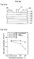
- Figure 5(a) is a cross-sectional view illustrating a structure of a prior art HEMT (high electron mobility transistor) which has an n type InAlAs carrier supply layer on an InP substrate and a Schottky formation layer on the n type InAlAs carrier supply layer.
- Figure 5(b) is a graph for explaining deterioration of electrical characteristics of the HEMT due to heat.
- reference numeral 101 designates a semi-insulating (abbreviated as S.I.- hereinafter) InP substrate
- reference numeral 102 designates an undoped InP layer of about 10 nm thickness
- reference numeral 103 designates an undoped InGaAs channel layer of about 20 nm thickness
- reference numeral 104 designates an undoped InAlAs spacer layer of about 3 nm thickness
- reference numeral 105 designates an n+ type InAlAs electron supply layer of about 15 nm thickness and to 3 x 1018 cm ⁇ 3 dopant impurity concentration
- reference numeral 106 designates a Schottky formation layer of about 10 nm thickness comprising materials such as undoped In 0.75 Ga 0.25 P
- reference numeral 107 designates an n+ type InGaAs ohmic layer of about 20 nm thickness and to 5 x 1018 cm ⁇ 3 dopant impurity concentration
- reference numeral 108 designates a source electrode
- abscissa represents heat treatment temperature (unit: °C) and ordinate represents sheet carrier concentration (unit: x 1012 cm ⁇ 3) of two-dimensional electron gas formed at the interface of the undoped InGaAs channel layer 103 to the undoped InAlAs spacer layer 104 side.
- circles, triangles, and squares represent cases where the Schottky formation layer 106 comprises In 0.75 Ga 0.25 P, InP, or InAlAs, respectively.
- Figure 6 illustrates a semiconductor layer structure used in the study by the inventors of the present invention and figure 7 illustrates the result obtained from this study.
- reference numeral 111 designates an S.I.-InP substrate
- reference numeral 112 designates an intrinsic (abbreviated as i- hereinafter) AlInAs buffer layer of 5000 ⁇ thickness
- reference numeral 113 designates an i-InGaAs channel layer of 2500 ⁇ thickness
- reference numeral 114 designates an AlInAs carrier supply layer of 340 ⁇ thickness in which a planar doping with Si is performed at 20 ⁇ elevation from the channel layer 113.
- a layer portion of the carrier supply layer 114 from the channel layer 113 to where the Si planar doping is performed is designated as a spacer layer 115.
- Reference numeral 116 designates two-dimensional electron gas formed in the vicinity of the interface of the i-GaInAs channel layer 113 to the InAlAs electron supply layer 114 side.
- abscissa represents heat treatment temperature (unit: °C) and ordinate represents a ratio of sheet carrier concentration N s after the heat treatment to that before the heat treatment N s0 , i.e., N s /N s0 .
- the semiconductor layer structure having the similar structure as an HEMT comprising the InAlAs electron supply layer 114 which was planar-doped with Si and was formed on the i-GaInAs channel layer 113 was heat-treated for fifteen minutes at different temperatures under a nitrogen environment. Then the sheet carrier concentration of the two-dimensional electron gas layer 116 formed in the vicinity of the interface of the i-GaInAs channel layer 113 to the electron supply layer 114 side was measured by Hall measurement. As illustrated in figure 7, even in the semiconductor layer structure such as this, the sheet carrier concentration decreases due to heat treatment and, by including a heat treatment process, an HEMT whose electrical characteristics are deteriorated is formed.
- a semiconductor device having an InAlAs layer doped with an impurity such as a prior art HEMT
- heat treatment is performed under an environment including carrier gas such as nitrogen gas or hydrogen gas
- carrier gas such as nitrogen gas or hydrogen gas
- the deterioration of electrical characteristics such as the decrease in the sheet carrier concentration occurs.
- a method of confirming changes of the characteristics in a lapse of time is used, in which the semiconductor device is operated under a high temperature environment in which the characteristics of the semiconductor device are likely to be deteriorated.
- the prior art semiconductor device when a reliability test including heat treatment such as this is conducted, the decrease in the sheet carrier concentration occurs and satisfactory results cannot be obtained. As a result, a semiconductor device of high reliability cannot be obtained.
- a method of fabricating a semiconductor device comprises forming a layer comprising Al, In, and As and doped with an impurity; infiltrating fluorine into the layer comprising Al, In, and As and doped with an impurity by performing heat treatment to this layer; and removing the fluorine from the layer comprising Al, In, and As and doped with an impurity by performing reheat treatment after the heat treatment.
- the layer comprising Al, In, and As can be recovered from a state of electrically deteriorated characteristics.
- the layer comprising Al, In, As and doped with an impurity having desired electrical characteristics can be obtained and re-deterioration of this layer can be prevented.
- the reheat treatment for removing the fluorine from the layer comprising Al, In, and As and doped with an impurity is performed either in vacuum or under any one environment selected from a group consisting of an environment supplied with nitrogen gas, an environment supplied with hydrogen gas, and an environment supplied with both nitrogen gas and hydrogen gas. Therefore, by removing the fluorine from the layer comprising Al, In, and As and doped with an impurity, this layer can be recovered from a state of electrically deteriorated characteristics caused by heat.
- the semiconductor device in the method of fabricating the semiconductor device described as the first aspect of the present invention, is a high electron mobility transistor; and the layer comprising Al, In, and As and doped with an impurity is a carrier supply layer of the high electron mobility transistor. Therefore, the carrier supply layer whose electrical characteristics are hard to be deteriorated can be obtained.
- a method of fabricating a semiconductor device comprises preparing a semi-insulating substrate; forming an undoped channel layer on the semi-insulating substrate; forming a carrier supply layer which comprises a layer comprising Al, In, and As and doped with an impurity on the channel layer; forming an ohmic layer on the carrier supply layer; forming a source electrode and a drain electrode on the ohmic layer; forming an opening by etching a portion of the ohmic layer between the source electrode and the drain electrode so that the carrier supply layer is exposed; infiltrating fluorine into the carrier supply layer by performing heat treatment to this carrier supply layer; removing the fluorine from the carrier supply layer by performing reheat treatment after the heat treatment; and forming a recess on the portion of the carrier supply layer exposed in the opening and, then, forming a gate electrode on the bottom of the recess. Therefore, the carrier supply layer whose electrical characteristics are hard to be deteriorated can be obtained.
- a semiconductor device has a layer comprising Al, In, and As and doped with an impurity wherein the layer comprising Al, In, and As and doped with an impurity is heat-treated so that fluorine is infiltrated into this layer and, then, reheat-treated so that the fluorine is removed from this layer. Therefore, a semiconductor device having a layer comprising Al, In, and As and doped with an impurity which has desired electrical characteristics, this electrical characteristics being hard to be deteriorated, can be obtained.
- Figure 1 is a cross-sectional view illustrating a semiconductor layer structure for describing a method of fabricating a semiconductor device according to a first embodiment of the present invention.
- Figures 2(a)-2(b) are graphs for describing the method of fabricating the semiconductor device according to the first embodiment of the present invention.
- Figure 3 is a graph for describing a method of fabricating a semiconductor device according to a second embodiment of the present invention.
- Figures 4(a)-4(c) are cross-sectional process views illustrating a method of fabricating an HEMT according to a third embodiment of the present invention.
- Figure 5(a) is a cross-sectional view illustrating a structure of an HEMT as an example of a prior art semiconductor device
- figure 5(b) is a graph illustrating a deterioration of electrical characteristics occurred due to heat treatment of the prior art HEMT.
- Figure 6 is a cross-sectional view illustrating a semiconductor layer structure for describing a deterioration of electrical characteristics of a semiconductor which occurs due to a heat treatment process in a method of fabricating a prior art semiconductor device.
- Figure 7 is a graph illustrating a relationship between a sheet carrier concentration and a heat treatment temperature for describing a deterioration of electrical characteristics of a semiconductor device which occurs due to a heat treatment process in a method of fabricating a prior art semiconductor device.
- Figure 8 is a cross-sectional view for describing a deterioration of electrical characteristics of a semiconductor device which occurs due to a heat treatment process in a method of fabricating a prior art semiconductor device.
- Figure 9 is a graph illustrating a fluorine profile for describing a deterioration of electrical characteristics of a semiconductor device which occurs due to a heat treatment process in a method of fabricating a prior art semiconductor device.
- Figure 10 is a graph illustrating a deterioration of electrical characteristics of a semiconductor device which occurs due to a heat treatment process at 200°C in a method of fabricating a prior art semiconductor device.
- Figure 11 is a graph illustrating a fluorine profile for describing a method of fabricating the semiconductor device according to the first embodiment of the present invention.
- Figure 12 is a graph illustrating a relationship between a change in fluorine concentration and a change in carrier concentration for describing a method of fabricating the semiconductor device according to the first embodiment of the present invention.
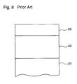
- Figure 8 is a cross-sectional view illustrating a semiconductor layer structure used in a study in search for causes of the deterioration of electrical characteristics of the prior art semiconductor device due to heat.
- reference numeral 21 designates an S.I.-InP substrate
- reference numeral 22 designates an i-AlInAs layer of about 4000 ⁇ thickness
- reference numeral 23 designates an AlInAs layer doped with Si as an impurity and of about 1300 ⁇ thickness.
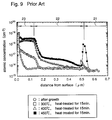
- abscissa represents a distance (unit: ⁇ m) from the surface of the semiconductor layer structure and ordinate represents an atomic concentration (unit: cm ⁇ 3) of fluorine.
- white circles represent a fluorine profile (distribution) of the semiconductor layer structure before the heat treatment, and white squares, white triangles, and black squares represent fluorine profiles for heat treatment temperatures of 300°C, 400°C, and 450°C, respectively.
- 19F fluorine infiltrates the semiconductor layer structure due to the heat treatment.
- the amount of 19F increases with the heat treatment temperatures.
- the infiltration amount of 19F is prominent in the Si-doped layer, and finally, 19F accumulates at the interface between the epitaxial layer and the substrate as well.
- the first fact above is based on the result obtained by detection of a mass number 19, checking for the entire mass of the impurity during SIMS measurement.
- the fluorine in the atmosphere sticks to and infiltrates the AlInAs layer 23 doped with Si because of the heat treatment and the change in profile due to the heat treatment is not observed for other elements, it is considered that the deterioration of electrical characteristics of a semiconductor device is caused by the phenomenon that the fluorine sticks to and infiltrates the semiconductor layer structure because of the heat treatment.
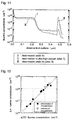
- Figure 10 is a graph illustrating a relationship between the carrier concentration of the Si-doped AlInAs layer 23 and the time duration of maintaining temperature when the semiconductor layer structure of figure 8 is heat-treated at a temperature of 200°C.
- ordinate represents the carrier concentration (unit: cm ⁇ 3)
- abscissa represents the time duration of maintaining temperature (hr).
- Figure 1 is a cross-sectional view for describing the main process of a method of fabricating a semiconductor device according to a first embodiment of the present invention.
- the method of fabricating the semiconductor device according to the first embodiment includes a process where reheat treatment is performed to an impurity-doped AlInAs layer which is deteriorated by fluorine infiltration due to the initial heat treatment, so that the fluorine in the impurity-doped AlInAs layer is removed and quality of the semiconductor device is recovered.
- reference numeral 1 designates an S.I.-InP substrate
- reference numeral 2 designates an i-AlInAs layer of about 2500 ⁇ thickness
- reference numeral 3 designates an Si-doped AlInAs layer of about 2500 ⁇ thickness.
- Figures 2(a)-2(b) are graphs illustrating results of Hall measurement of the semiconductor layer structure illustrated in figure 1 which is formed through the main process of the method of fabricating the semiconductor device of the first embodiment.
- Figure 2(a) indicates a relationship between a heat treatment duration (unit: second) for the semiconductor layer structure illustrated in figure 1 and a carrier concentration n (unit: cm ⁇ 3) and figure 2(b) indicates a relationship between the heat treatment duration (unit: second) and the electron mobility ⁇ (unit: cm2/Vs).
- circles with slashed lines represent a state before the heat treatment
- black circles represent a case where heat treatment is performed under an environment supplied with nitrogen gas
- white circles represent a case where heat treatment is performed in ultra-high vacuum.
- ordinate represents fluorine concentration (unit: cm ⁇ 3)
- abscissa represents a distance from the surface (unit: ⁇ m)
- a solid line represents the profile of step I in figures 2(a)-2(b)
- a dashed line represents the profile of step II
- an alternate long and short dashed line represents the profile of step III. Therefore, it can be said that if the fluorine concentration decreases, the carrier concentration n and the electron mobility ⁇ recover.
- a semiconductor device having desired electrical characteristics in a method of fabricating a semiconductor device including a process of infiltrating fluorine into the Si-doped AlInAs layer 3 by heat treatment, by having a process of removing the fluorine in the Si-doped AlInAs layer 3 by further heat treatment in the ultra-high vacuum after the initial heat treatment, a semiconductor device having desired electrical characteristics can be obtained.
- the Si-doped AlInAs layer 3 becomes hard to be deteriorated again and a highly-reliable semiconductor device which is hard to be deteriorated can be obtained.
- the method of fabricating the semiconductor device includes a process of infiltrating the fluorine into the Si-doped AlInAs layer 3 by the heat treatment under the nitrogen environment after the Si-doped AlInAs layer 23 is made to contact with the atmosphere and a process of removing the fluorine in the Si-doped AlInAs layer 3 by further heat treatment in the ultra-high vacuum after the initial heat treatment, a highly-reliable semiconductor device which is hard to be deteriorated again and has desired electrical characteristics can be obtained.
- this invention can be applied to the case where the impurity doped into the AlInAs layer is other impurities such as Sn (tin) and the similar effect as in the first embodiment can be obtained in this case.
- this invention can be applied to a case where this heat treatment is performed under environments supplied with other carrier gases such as hydrogen and the similar effect as in the first embodiment can be obtained in this case.
- Figure 3 is for describing a method of fabricating a semiconductor device according to a second embodiment of the present invention. While, in the first embodiment, the case where the reheat treatment for removing the fluorine which infiltrated into the impurity-doped AlInAs layer due to the initial heat treatment is performed in the ultra-high vacuum, this reheat treatment in the second embodiment is performed under an environment supplied with hydrogen gas or nitrogen gas.
- Figure 3 shows the time duration of the reheat treatment (unit: minute) required for the carrier concentration of the Si-doped AlInAs layer 3 of the semiconductor layer structure shown in figure 1 which was deteriorated by heat to recover to half the carrier concentration before the deterioration by heat for the cases where the reheat treatment environments are the environments supplied with hydrogen gas or nitrogen gas, or the ultra-high vacuum environment.
- the treatment temperature of the reheat treatment is 400°C.
- the carrier concentration recovers. Therefore, it can be seen that even when the reheat treatment under the environments such as these is performed, the semiconductor layer structure can be recovered from the deteriorated state caused by heat and a semiconductor device which has less deterioration of electrical characteristics due to heat is obtained.
- the figure also shows that the reheat treatment in the ultra-high vacuum takes least time for the recovery from the deterioration and the reheat treatment under the nitrogen gas environment takes the most time for the recovery.
- the method of fabricating the semiconductor device of the second embodiment since there is no need to use the ultra-high vacuum state, it is possible to perform a heat treatment process of removing the fluorine by using, for example, a nitrogen vessel of simple construction equipped with a means for heating up and a means for continuously supplying nitrogen, and a semiconductor device having desired characteristics can be obtained at low cost.
- the heat treatment is performed under the environment supplied with either hydrogen gas or nitrogen gas
- the heat treatment can also be performed under the environment supplied with the mixture of the hydrogen gas and the nitrogen gas in this invention, and the similar effect as in the second embodiment can be obtained in this case.
- Figures 4(a)-4(c) are cross-sectional views illustrating a method of fabricating an HEMT according to a third embodiment of the present invention using the method of fabricating the semiconductor device described in the first embodiment.
- reference numeral 11 designates an S.I.-InP substrate
- reference numeral 12 designates an AlInAs buffer layer of about 2500 ⁇ thickness
- reference numeral 13 designates an undoped InGaAs channel layer of about 500 ⁇ thickness
- reference numeral 14 designates an AlInAs carrier supply layer of about 340 ⁇ thickness in which an impurity such as Si is planar-doped (14a) at the elevation of 20 ⁇ from the InGaAs channel layer 13.
- Reference numeral 16 designates an n type InGaAs ohmic layer of about 500 ⁇ thickness
- reference numeral 16a designates an opening formed on the n type InGaAs ohmic layer
- reference numeral 17 designates a source electrode
- reference numeral 18 designates a drain electrode
- reference numeral 19 designates an EB (electron beam) resist used to form a recess groove
- reference numeral 20 is a photoresist used to form a gate electrode 24.
- the AlInAs layer 12 and the InGaAs channel layer 13 are successively formed on the InP substrate 11 inside an MBE (molecular beam epitaxy) chamber. Then the AlInAs layer of about 20 ⁇ thickness is formed, and after the Si planar doping 14a is performed, the AlInAs layer of about 320 ⁇ thickness is formed, thereby forming the AlInAs carrier supply layer 14. Then the n type InGaAs ohmic layer 16 is disposed and the semiconductor layer structure is obtained.
- MBE molecular beam epitaxy
- the semiconductor layer structure is taken out from the MBE chamber and the source electrode 17 and the drain electrode 18 are formed by evaporation and lift-off.
- an EB resist (not shown in the figures) is formed on the surface of the semiconductor layer structure and patterning is performed with an EB (electron beam) exposure.
- EB electron beam
- a portion of the n type InGaAs ohmic layer 16 between the source electrode 17 and the drain electrode 18 is removed by selective etching using an etchant comprising water added with hydrogen peroxide (H2O2) and organic acid, thereby forming the opening 16a.
- the EB resist is then removed (figure 4(a)).
- the AlInAs carrier supply layer 14 is exposed through the opening and fluorine sticks to the surface of the AlInAs carrier supply layer 14.
- the fluorine stuck to the surface of the AlInAs carrier supply layer 14 is infiltrated into the AlInAs carrier supply layer 14, and then heat treatment in the ultra-high vacuum is performed to remove the fluorine.
- the EB resist 19 and the photoresist 20 are formed on the surface of the semiconductor layer structure, and stepper light exposure is performed on the photoresist 20 so that a portion of the photoresist 20 between the source electrode 17 and the drain electrode 18 is removed to form an opening.
- EB exposure is performed on a portion of the EB resist 19 over the opening 16a within the opening of the photoresist 20, thereby forming an opening in the EB resist 19.
- etching is performed on the AlInAs carrier supply layer 14 using an etchant comprising water added with hydrogen peroxide and phosphoric acid (H3PO4) to form a recess (figure 4(b)).
- a gate metal is formed on the surface of the semiconductor layer structure by evaporation.
- the EB resist 19 and the photoresist 20 are then removed and the gate electrode 24 is formed by lifting off the unnecessary gate metal, thereby obtaining the HEMT illustrated in figure 4(c).
- the HEMT according to the third embodiment is a transistor which makes the high speed operation possible by the two-dimensional electron gas of high electron mobility generated at the interface of the InGaAs channel layer 13 to the AlInAs carrier supply layer 14 side by joining the AlInAs carrier supply layer 14 onto the InGaAs channel layer 13. Since the prior art method of fabrication does not include the heat treatment process described in the first embodiment after the process illustrated in figure 4(a), the fluorine stuck to the surface of the AlInAs carrier supply layer 14 infiltrates the carrier supply layer. Consequently, the carrier supply layer 14 becomes deteriorated during the operation of the HEMT. The sheet carrier concentration of the two-dimensional electron gas also decreases and the HEMT having desired characteristics cannot be obtained.
- MTTF mean time to failure
- the opening 16a for forming the recess is formed in the n type InGaAs ohmic layer 16, and the AlInAs carrier supply layer 14 is made to contact with the atmosphere. And then by performing the heat treatment as described in the first embodiment, the fluorine is infiltrated into the AlInAs carrier supply layer 14. By further adding a process of removing the fluorine in the ultra-high vacuum, the AlInAs carrier supply layer 14 can be made hard to be deteriorated, and the highly-reliable HEMT can be obtained.
- the HEMT having MTTF of more than 106 hours at 170°C which is an improvement by three digits from a prior art HEMT, can be obtained.
- the method of fabrication includes a process of infiltrating fluorine into the AlInAs carrier supply layer planar-doped with Si and a process of removing the fluorine by heat treatment in the ultra-high vacuum. Therefore, the highly-reliable HEMT can be provided.
- the heat treatment for removing the fluorine is performed in the ultra-high vacuum
- the heat treatment can be performed under the nitrogen gas environment or the hydrogen gas environment in this invention as described in the second embodiment, and the similar effect can be obtained as in the third embodiment.
- the opening is formed in the n type InGaAs ohmic layer 16 to form the recess and the AlInAs carrier supply layer 14 is made to contact with the atmosphere. Then the heat treatment for infiltrating in and removing the fluorine is performed.
- the AlInAs carrier supply layer 14 is formed, a process of making the AlInAs carrier supply layer 14 to contact with the atmosphere and then performing the heat treatment can be performed at any step, and the similar effect as in the third embodiment can be obtained.
Abstract
Description
- The present invention relates to a method of fabricating a semiconductor device for improving reliability of a semiconductor device, and a semiconductor device fabricated thereby.
- Figures 5(a)-5(b) were shown in Extended Abstract WC2 pp497-500 of Fifth International Conference on Indium Phosphide and Related Materials, held from April 19 to 22, 1993 in Paris, France. Figure 5(a) is a cross-sectional view illustrating a structure of a prior art HEMT (high electron mobility transistor) which has an n type InAlAs carrier supply layer on an InP substrate and a Schottky formation layer on the n type InAlAs carrier supply layer. Figure 5(b) is a graph for explaining deterioration of electrical characteristics of the HEMT due to heat.
- In figure 5(a),
reference numeral 101 designates a semi-insulating (abbreviated as S.I.- hereinafter) InP substrate,reference numeral 102 designates an undoped InP layer of about 10 nm thickness,reference numeral 103 designates an undoped InGaAs channel layer of about 20 nm thickness,reference numeral 104 designates an undoped InAlAs spacer layer of about 3 nm thickness,reference numeral 105 designates an n⁺ type InAlAs electron supply layer of about 15 nm thickness and to 3 x 10¹⁸ cm⁻³ dopant impurity concentration,reference numeral 106 designates a Schottky formation layer of about 10 nm thickness comprising materials such as undoped In0.75Ga0.25P,reference numeral 107 designates an n⁺ type InGaAs ohmic layer of about 20 nm thickness and to 5 x 10¹⁸ cm⁻³ dopant impurity concentration,reference numeral 108 designates a source electrode,reference numeral 109 designates a drain electrode, andreference numeral 110 designates a gate electrode. - In figure 5(b), abscissa represents heat treatment temperature (unit: °C) and ordinate represents sheet carrier concentration (unit: x 10¹² cm⁻³) of two-dimensional electron gas formed at the interface of the undoped
InGaAs channel layer 103 to the undopedInAlAs spacer layer 104 side. In the figure, circles, triangles, and squares represent cases where the Schottkyformation layer 106 comprises In0.75Ga0.25P, InP, or InAlAs, respectively. - Deterioration of electrical characteristics of an HEMT due to heat will be described as follows. In the above reference, Fujita, who is the author of the reference, and others prepared three different semiconductor layer structures whose main part is similar to that of the HEMT illustrated in figure 5(a) comprising the
undoped InP layer 102, the undoped InGaAschannel layer 103, the undopedInAlAs spacer layer 104, the n⁺ type InAlAselectron supply layer 105, and the Schottkyformation layer 106 comprising any one material from a group consisting of In0.75Ga0.25P, InP, and InAlAs grown in this order on thesemiconductor substrate 101. These semiconductor layer structures are heat-treated for five minutes at temperatures of 300°C or 350°C under an environment supplied with nitrogen gas, and sheet carrier concentrations of the two-dimensional electron gas formed at the interface of the undopedInGaAs channel layer 103 to the undopedInAlAs spacer layer 104 side are measured. The results are as illustrated in figure 5(b). From the figure, regardless of the material for theelectrode layer 106, which is any one of a group consisting of the In0.75Ga0.25P, the InP, and the InAlAs, the sheet carrier concentrations decrease after the heat treatment at a temperature of 300°C or above. - These results indicate that, if heat treatment at a temperature of 300°C or above is performed, the electrical characteristics of an HEMT are deteriorated by heat and a desired sheet carrier concentration cannot be obtained. As a result, a resistance of the region where the two-dimensional electron gas is formed increases and the expected HEMT characteristics cannot be obtained. Concerning to this phenomenon, Fujita et al commented that this decrease in the surface sheet carrier concentration was due to an increase in a surface depletion layer caused by surface deterioration of the InAlAs layer.
- The inventors of the present invention have also studied the deterioration of electrical characteristics of an HEMT due to heat. Figure 6 illustrates a semiconductor layer structure used in the study by the inventors of the present invention and figure 7 illustrates the result obtained from this study. In figure 6,
reference numeral 111 designates an S.I.-InP substrate,reference numeral 112 designates an intrinsic (abbreviated as i- hereinafter) AlInAs buffer layer of 5000 Å thickness,reference numeral 113 designates an i-InGaAs channel layer of 2500 Å thickness, andreference numeral 114 designates an AlInAs carrier supply layer of 340 Å thickness in which a planar doping with Si is performed at 20 Å elevation from thechannel layer 113. A layer portion of thecarrier supply layer 114 from thechannel layer 113 to where the Si planar doping is performed is designated as aspacer layer 115.Reference numeral 116 designates two-dimensional electron gas formed in the vicinity of the interface of the i-GaInAschannel layer 113 to the InAlAselectron supply layer 114 side. - In figure 7, abscissa represents heat treatment temperature (unit: °C) and ordinate represents a ratio of sheet carrier concentration Ns after the heat treatment to that before the heat treatment Ns0, i.e., Ns/Ns0.
- This study was carried out as follows. The semiconductor layer structure having the similar structure as an HEMT comprising the InAlAs
electron supply layer 114 which was planar-doped with Si and was formed on the i-GaInAschannel layer 113 was heat-treated for fifteen minutes at different temperatures under a nitrogen environment. Then the sheet carrier concentration of the two-dimensionalelectron gas layer 116 formed in the vicinity of the interface of the i-GaInAs channel layer 113 to theelectron supply layer 114 side was measured by Hall measurement. As illustrated in figure 7, even in the semiconductor layer structure such as this, the sheet carrier concentration decreases due to heat treatment and, by including a heat treatment process, an HEMT whose electrical characteristics are deteriorated is formed. - As described above, in a semiconductor device having an InAlAs layer doped with an impurity such as a prior art HEMT, if heat treatment is performed under an environment including carrier gas such as nitrogen gas or hydrogen gas, the deterioration of electrical characteristics such as the decrease in the sheet carrier concentration occurs. Usually, in order to confirm the reliability of a semiconductor device, a method of confirming changes of the characteristics in a lapse of time is used, in which the semiconductor device is operated under a high temperature environment in which the characteristics of the semiconductor device are likely to be deteriorated. However, in the prior art semiconductor device, when a reliability test including heat treatment such as this is conducted, the decrease in the sheet carrier concentration occurs and satisfactory results cannot be obtained. As a result, a semiconductor device of high reliability cannot be obtained.
- Furthermore, since the characteristics are deteriorated by heat as described above, it is extremely difficult to operate the prior art semiconductor device at a high temperature for a long period of time while maintaining desired characteristics. It is also difficult to provide a semiconductor device which has high reliability against the high temperature operation.
- Furthermore, if a heat treatment process at high temperature is necessary after the formation of an InAlAs layer doped with an impurity in a method of fabricating the prior art semiconductor device, the electrical characteristics of this InAlAs layer doped with an impurity are deteriorated by heat and a semiconductor device with desired characteristics cannot be obtained. For example, in an HEMT having an InAlAs layer doped with an impurity as a carrier supply layer, if the deterioration due to heat like this occurs, the sheet carrier concentration of two-dimensional electron gas decreases and desired operational characteristics cannot be obtained.
- It is an object of the present invention to provide a method of fabricating a highly-reliable semiconductor device having desired electrical characteristics.
- It is another object of the present invention to provide a highly-reliable semiconductor device having desired electrical characteristics fabricated thereby.
other objects and advantages of the invention will become apparent from the detailed description that follows. The detailed description and specific embodiments described are provided only for illustration since various additions and modifications within the scope of the invention will be apparent to those of skill in the art from the detailed description. - According to a first aspect of the present invention, a method of fabricating a semiconductor device comprises forming a layer comprising Al, In, and As and doped with an impurity; infiltrating fluorine into the layer comprising Al, In, and As and doped with an impurity by performing heat treatment to this layer; and removing the fluorine from the layer comprising Al, In, and As and doped with an impurity by performing reheat treatment after the heat treatment. Therefore, in a method of fabricating a semiconductor device, for example, where a process of infiltrating fluorine into the layer comprising Al, In, and As and doped with an impurity by performing heat treatment is not necessary, by actively infiltrating fluorine into the this layer comprising Al, In, and As and doped with an impurity by heat treatment and then removing the fluorine by performing further heat treatment, electrical characteristics of the layer comprising Al, In, and As and doped with an impurity can be made hard to be deteriorated.
- Furthermore, in a method of fabricating a semiconductor device including a process of infiltrating fluorine by heat treatment, by performing heat treatment to remove the fluorine after the process of infiltrating the fluorine, the layer comprising Al, In, and As can be recovered from a state of electrically deteriorated characteristics. As a result, the layer comprising Al, In, As and doped with an impurity having desired electrical characteristics can be obtained and re-deterioration of this layer can be prevented.
- According to a second aspect of the present invention, in the method of fabricating the semiconductor device described as the first aspect of the present invention, the reheat treatment for removing the fluorine from the layer comprising Al, In, and As and doped with an impurity is performed either in vacuum or under any one environment selected from a group consisting of an environment supplied with nitrogen gas, an environment supplied with hydrogen gas, and an environment supplied with both nitrogen gas and hydrogen gas. Therefore, by removing the fluorine from the layer comprising Al, In, and As and doped with an impurity, this layer can be recovered from a state of electrically deteriorated characteristics caused by heat.
- According to a third aspect of the present invention, in the method of fabricating the semiconductor device described as the first aspect of the present invention, the semiconductor device is a high electron mobility transistor; and the layer comprising Al, In, and As and doped with an impurity is a carrier supply layer of the high electron mobility transistor. Therefore, the carrier supply layer whose electrical characteristics are hard to be deteriorated can be obtained.
- According to a fourth aspect of the present invention, a method of fabricating a semiconductor device comprises preparing a semi-insulating substrate; forming an undoped channel layer on the semi-insulating substrate; forming a carrier supply layer which comprises a layer comprising Al, In, and As and doped with an impurity on the channel layer; forming an ohmic layer on the carrier supply layer; forming a source electrode and a drain electrode on the ohmic layer; forming an opening by etching a portion of the ohmic layer between the source electrode and the drain electrode so that the carrier supply layer is exposed; infiltrating fluorine into the carrier supply layer by performing heat treatment to this carrier supply layer; removing the fluorine from the carrier supply layer by performing reheat treatment after the heat treatment; and forming a recess on the portion of the carrier supply layer exposed in the opening and, then, forming a gate electrode on the bottom of the recess. Therefore, the carrier supply layer whose electrical characteristics are hard to be deteriorated can be obtained.
- According to a fifth aspect of the present invention, a semiconductor device has a layer comprising Al, In, and As and doped with an impurity wherein the layer comprising Al, In, and As and doped with an impurity is heat-treated so that fluorine is infiltrated into this layer and, then, reheat-treated so that the fluorine is removed from this layer. Therefore, a semiconductor device having a layer comprising Al, In, and As and doped with an impurity which has desired electrical characteristics, this electrical characteristics being hard to be deteriorated, can be obtained.
- Figure 1 is a cross-sectional view illustrating a semiconductor layer structure for describing a method of fabricating a semiconductor device according to a first embodiment of the present invention.
- Figures 2(a)-2(b) are graphs for describing the method of fabricating the semiconductor device according to the first embodiment of the present invention.
- Figure 3 is a graph for describing a method of fabricating a semiconductor device according to a second embodiment of the present invention.
- Figures 4(a)-4(c) are cross-sectional process views illustrating a method of fabricating an HEMT according to a third embodiment of the present invention.
- Figure 5(a) is a cross-sectional view illustrating a structure of an HEMT as an example of a prior art semiconductor device, and figure 5(b) is a graph illustrating a deterioration of electrical characteristics occurred due to heat treatment of the prior art HEMT.
- Figure 6 is a cross-sectional view illustrating a semiconductor layer structure for describing a deterioration of electrical characteristics of a semiconductor which occurs due to a heat treatment process in a method of fabricating a prior art semiconductor device.
- Figure 7 is a graph illustrating a relationship between a sheet carrier concentration and a heat treatment temperature for describing a deterioration of electrical characteristics of a semiconductor device which occurs due to a heat treatment process in a method of fabricating a prior art semiconductor device.
- Figure 8 is a cross-sectional view for describing a deterioration of electrical characteristics of a semiconductor device which occurs due to a heat treatment process in a method of fabricating a prior art semiconductor device.
- Figure 9 is a graph illustrating a fluorine profile for describing a deterioration of electrical characteristics of a semiconductor device which occurs due to a heat treatment process in a method of fabricating a prior art semiconductor device.
- Figure 10 is a graph illustrating a deterioration of electrical characteristics of a semiconductor device which occurs due to a heat treatment process at 200°C in a method of fabricating a prior art semiconductor device.
- Figure 11 is a graph illustrating a fluorine profile for describing a method of fabricating the semiconductor device according to the first embodiment of the present invention.
- Figure 12 is a graph illustrating a relationship between a change in fluorine concentration and a change in carrier concentration for describing a method of fabricating the semiconductor device according to the first embodiment of the present invention.
- Figure 8 is a cross-sectional view illustrating a semiconductor layer structure used in a study in search for causes of the deterioration of electrical characteristics of the prior art semiconductor device due to heat. In the figure,
reference numeral 21 designates an S.I.-InP substrate,reference numeral 22 designates an i-AlInAs layer of about 4000 Å thickness,reference numeral 23 designates an AlInAs layer doped with Si as an impurity and of about 1300 Å thickness. - This study was conducted as follows. The semiconductor layer structures as shown in figure 8 in which the i-
AlInAs layer 22 and theAlInAs layer 23 which was planar-doped with Si were successively formed on the S.I.-InP substrate 21 in an MBE (molecular beam epitaxy) chamber were taken out from the chamber, and then the semiconductor structures were heat-treated for fifteen minutes under a nitrogen environment at 300°C for one of them, 400°C for another one of them, and 450°C for yet another one of them. And then impurity analysis of the semiconductor layer structure was made by SIMS (secondary ion mass spectroscopy). The result of the impurity analysis is illustrated in figure 9. - In figure 9, abscissa represents a distance (unit: µm) from the surface of the semiconductor layer structure and ordinate represents an atomic concentration (unit: cm⁻³) of fluorine. In the figure, white circles represent a fluorine profile (distribution) of the semiconductor layer structure before the heat treatment, and white squares, white triangles, and black squares represent fluorine profiles for heat treatment temperatures of 300°C, 400°C, and 450°C, respectively.
- From the study, the following facts are ascertained. First, ¹⁹F (fluorine) infiltrates the semiconductor layer structure due to the heat treatment. Secondly, the amount of ¹⁹F increases with the heat treatment temperatures. Thirdly, the infiltration amount of ¹⁹F is prominent in the Si-doped layer, and finally, ¹⁹F accumulates at the interface between the epitaxial layer and the substrate as well. The first fact above is based on the result obtained by detection of a
mass number 19, checking for the entire mass of the impurity during SIMS measurement. - From the above first, second, third, and fourth facts, a new fact that the fluorine (¹⁹F) infiltrates the semiconductor layer structure due to heat treatment, which had not previously been known, was ascertained. Since the fluorine was not detected at all from materials except the
AlInAs layer 23 which was doped with Si, it was considered that the phenomenon that the fluorine infiltrated the semiconductor layer was characteristic only to theAlInAs layer 23 which was doped with an impurity such as Si. The infiltrating route of the fluorine was investigated, but the fluorine was not used in the growth chamber for MBE or MOCVD or the like used for the growth of the semiconductor layer structure, and the fluorine was not actively supplied inside the laboratory, either. When the uppermost surface of the Si-dopedAlInAs layer 23 right after the growth was analyzed by ESCA (electron spectroscopy for chemical analysis), about 0.3 atomic % of fluorine was detected. From this, it was considered that fluorine resulted from fluoric acid (HF) or the like used in semiconductor fabricating processes remained in the air inside the laboratory, and this minute amount of fluorine, when the uppermost surface of the Si-dopedAlInAs layer 23 was exposed to the atmosphere, was attracted to and stuck to the surface, and resulted in the infiltration into theAlInAs layer 23. - Together with this analysis on the fluorine, although not shown in the figure, changes of the profile in a lapse of time before and after the heat treatment were investigated for elements besides fluorine such as nitrogen, and the results were obtained that almost the same profiles were obtained before and after the heat treatment.
- As described above, since the fluorine in the atmosphere sticks to and infiltrates the
AlInAs layer 23 doped with Si because of the heat treatment and the change in profile due to the heat treatment is not observed for other elements, it is considered that the deterioration of electrical characteristics of a semiconductor device is caused by the phenomenon that the fluorine sticks to and infiltrates the semiconductor layer structure because of the heat treatment. - In order to prevent this deterioration due to the infiltration of the fluorine, one of the choices is to remove the fluorine left in the atmosphere entirely. However, the fluorine in the atmosphere in a plant where semiconductors are fabricated cannot usually be removed entirely but remains. A perfect removal would be extremely difficult and it is considered to be difficult to prevent the fluorine infiltration.
- Therefore, as long as there is the phenomenon that due to the heat treatment the fluorine infiltrates through the surface of the AlInAs layer doped with an impurity such as Si which makes a contact with the atmosphere, the deterioration of the semiconductor device having the AlInAs layer doped with an impurity because of the heat treatment cannot be avoided.
- Furthermore, even though the heat treatment temperature is below the temperature selected in the above study, it is confirmed that the deterioration due to heat becomes pronounced by maintaining the temperature for a long period of time. Figure 10 is a graph illustrating a relationship between the carrier concentration of the Si-doped
AlInAs layer 23 and the time duration of maintaining temperature when the semiconductor layer structure of figure 8 is heat-treated at a temperature of 200°C. In the figure, ordinate represents the carrier concentration (unit: cm⁻³) and abscissa represents the time duration of maintaining temperature (hr). As can be seen from figure 10, even in the heat treatment at a low temperature of 200°C, the carrier concentration decreases by maintaining the temperature for 100 hours or more. This indicates that the thermal deterioration of the semiconductor device occurs at such a temperature as selected above and, at the same time, there is a possibility that the semiconductor device becomes deteriorated over a long period of time even at a temperature lower than the above temperature, indicating that the reliability of the semiconductor device is extremely poor. - Figure 1 is a cross-sectional view for describing the main process of a method of fabricating a semiconductor device according to a first embodiment of the present invention. The method of fabricating the semiconductor device according to the first embodiment includes a process where reheat treatment is performed to an impurity-doped AlInAs layer which is deteriorated by fluorine infiltration due to the initial heat treatment, so that the fluorine in the impurity-doped AlInAs layer is removed and quality of the semiconductor device is recovered. In figure 1,
reference numeral 1 designates an S.I.-InP substrate,reference numeral 2 designates an i-AlInAs layer of about 2500 Å thickness, andreference numeral 3 designates an Si-doped AlInAs layer of about 2500 Å thickness. - Figures 2(a)-2(b) are graphs illustrating results of Hall measurement of the semiconductor layer structure illustrated in figure 1 which is formed through the main process of the method of fabricating the semiconductor device of the first embodiment. Figure 2(a) indicates a relationship between a heat treatment duration (unit: second) for the semiconductor layer structure illustrated in figure 1 and a carrier concentration n (unit: cm⁻³) and figure 2(b) indicates a relationship between the heat treatment duration (unit: second) and the electron mobility µ (unit: cm²/Vs). In the figures, circles with slashed lines represent a state before the heat treatment, black circles represent a case where heat treatment is performed under an environment supplied with nitrogen gas, and white circles represent a case where heat treatment is performed in ultra-high vacuum.
- The main process of the method of fabricating the semiconductor device according to the first embodiment will be described with reference to figure 1.
- First, the i-
AlInAs layer 2 and the Si-dopedAlInAs layer 3 are successively formed on the S.I.-InP semiconductor substrate 1 inside an MBE chamber, thereby obtaining the semiconductor layer structure which serves as a sample as shown in figure 1. Then the semiconductor layer structure is taken out from the MBE chamber. The Hall measurement was performed on the sample then and the sheet carrier concentration of the Si-dopedAlInAs layer 3 was n = 4 x 10¹⁸ cm⁻³ and the electron mobility at 300 K was µ(300 K) = 500 cm²/Vs. - Next, electrical characteristics of the sample is deteriorated by heat-treating the sample for 18 minutes at 400°C under a nitrogen environment. The Hall measurement was again performed then. The carrier concentration was n = 8 x 10¹⁶ cm⁻³ and the electron mobility was µ(300 K) = 320 cm²/Vs. Both the carrier concentration and the electron mobility decrease and it can be seen that the electrical characteristics of the sample are in a deteriorated state due to heat.
- Next, the sample whose characteristics were deteriorated by the heat is placed in the MBE chamber and heat-treated for seven minutes at 400°C in the ultra-high vacuum in order to exclude the infiltrated fluorine from the sample. For both the carrier concentration n and the electron mobility µ, values were recovered from the deteriorated states caused by the heat treatment, and by performing similar treatment continuously, they recovered further (figures 2(a)-2(b)). Fluorine profile was measured then by SIMS measurement and it was revealed that the fluorine concentration decreased when heat treatment was performed in the ultra-high vacuum in contrast to a state where characteristics were deteriorated by heat as shown in figure 11. In figure 11, ordinate represents fluorine concentration (unit: cm⁻³), abscissa represents a distance from the surface (unit: µm), a solid line represents the profile of step I in figures 2(a)-2(b), a dashed line represents the profile of step II, and an alternate long and short dashed line represents the profile of step III. Therefore, it can be said that if the fluorine concentration decreases, the carrier concentration n and the electron mobility µ recover.
- Furthermore, the increase in the fluorine concentration and the decrease in the carrier concentration during the deterioration of electrical characteristics of the Si-doped
AlInAs layer 3 due to heat, and the decrease in the fluorine concentration and the increase in the carrier concentration during recovery of the characteristics by heat treatment in the ultra-high vacuum are presented in a graph with logarithmic scales in figure 12, abscissa representing the absolute value of the change in the fluorine concentration and ordinate representing the absolute value of the change in the carrier concentration. In figure 12, black circles represent values during deterioration of characteristics due to heat and white circles represent values during recovery from the deterioration of the characteristics. As can be seen, it is understood that the change in the fluorine concentration and the change in the carrier concentration have a certain relationship. - The above results illustrate that by again heat-treating in the ultra-high vacuum after the characteristics deterioration due to heat, the fluorine can be excluded from the Si-doped
AlInAs layer 3 and the Si-dopedAlInAs layer 3 can be recovered from the state of the electrical characteristics deterioration due to heat treatment, thereby recovering the semiconductor device from the state in which electrical characteristics are deteriorated. Therefore, in a method of fabricating a semiconductor device including a process of infiltrating fluorine into the Si-dopedAlInAs layer 3 by heat treatment, by having a process of removing the fluorine in the Si-dopedAlInAs layer 3 by further heat treatment in the ultra-high vacuum after the initial heat treatment, a semiconductor device having desired electrical characteristics can be obtained. - Furthermore, after the heat treatment in the ultra-high vacuum, the environment was replaced with the one supplied with nitrogen gas, and it was again tried to deteriorate the semiconductor layer structure by heat. However, the carrier concentration n did not decrease as shown in figures 2(a)-2(b), and the fluorine profile did not increase as shown in figure 11 and the deterioration due to reheating did not occur, revealing that the sample had durability against another heat treatment in nitrogen once the sample entered the recovery cycle, i.e., the sample was stable against heat treatment. Therefore, by heat-treating the Si-doped
AlInAs layer 3 in the ultra-high vacuum which was once deteriorated by heat, the Si-dopedAlInAs layer 3 becomes hard to be deteriorated again and a highly-reliable semiconductor device which is hard to be deteriorated can be obtained. - Furthermore, using a tendency that the Si-doped
AlInAs layer 3 in the recovery cycle becomes hard to be deteriorated again as described above, after the Si-dopedlayer 3 is made to contact with the atmosphere, heat treatment is performed so that fluorine actively infiltrates the Si-dopedlayer 3 and characteristics are deteriorated. Then by performing reheat treatment until the fluorine profile is stabilized, it is possible to obtain a highly-reliable semiconductor device which is hard to be deteriorated and is sufficiently durable in high temperature reliability test. - Since the method of fabricating the semiconductor device according to this embodiment includes a process of infiltrating the fluorine into the Si-doped
AlInAs layer 3 by the heat treatment under the nitrogen environment after the Si-dopedAlInAs layer 23 is made to contact with the atmosphere and a process of removing the fluorine in the Si-dopedAlInAs layer 3 by further heat treatment in the ultra-high vacuum after the initial heat treatment, a highly-reliable semiconductor device which is hard to be deteriorated again and has desired electrical characteristics can be obtained. - While, in this first embodiment, a case where the impurity doped into the
AlInAs layer 3 is Si is described, this invention can be applied to the case where the impurity doped into the AlInAs layer is other impurities such as Sn (tin) and the similar effect as in the first embodiment can be obtained in this case. - While, in this first embodiment, the heat treatment which infiltrates the fluorine into the Si-doped
AlInAs layer 3 is performed under the nitrogen environment, this invention can be applied to a case where this heat treatment is performed under environments supplied with other carrier gases such as hydrogen and the similar effect as in the first embodiment can be obtained in this case. - Figure 3 is for describing a method of fabricating a semiconductor device according to a second embodiment of the present invention. While, in the first embodiment, the case where the reheat treatment for removing the fluorine which infiltrated into the impurity-doped AlInAs layer due to the initial heat treatment is performed in the ultra-high vacuum, this reheat treatment in the second embodiment is performed under an environment supplied with hydrogen gas or nitrogen gas. Figure 3 shows the time duration of the reheat treatment (unit: minute) required for the carrier concentration of the Si-doped
AlInAs layer 3 of the semiconductor layer structure shown in figure 1 which was deteriorated by heat to recover to half the carrier concentration before the deterioration by heat for the cases where the reheat treatment environments are the environments supplied with hydrogen gas or nitrogen gas, or the ultra-high vacuum environment. The treatment temperature of the reheat treatment is 400°C. - As shown in figure 3, even in the reheat treatment under the environment supplied with the hydrogen gas or the nitrogen gas, the carrier concentration recovers. Therefore, it can be seen that even when the reheat treatment under the environments such as these is performed, the semiconductor layer structure can be recovered from the deteriorated state caused by heat and a semiconductor device which has less deterioration of electrical characteristics due to heat is obtained. The figure also shows that the reheat treatment in the ultra-high vacuum takes least time for the recovery from the deterioration and the reheat treatment under the nitrogen gas environment takes the most time for the recovery.
- In the method of fabricating the semiconductor device according to this embodiment, since a process of removing the fluorine in the Si-doped
AlInAs layer 3 by heat treatment is performed under the environment supplied with either hydrogen gas or nitrogen gas, the similar effect as in the first embodiment is obtained. - Furthermore, according to the method of fabricating the semiconductor device of the second embodiment, since there is no need to use the ultra-high vacuum state, it is possible to perform a heat treatment process of removing the fluorine by using, for example, a nitrogen vessel of simple construction equipped with a means for heating up and a means for continuously supplying nitrogen, and a semiconductor device having desired characteristics can be obtained at low cost.
- While, in the second embodiment, the heat treatment is performed under the environment supplied with either hydrogen gas or nitrogen gas, the heat treatment can also be performed under the environment supplied with the mixture of the hydrogen gas and the nitrogen gas in this invention, and the similar effect as in the second embodiment can be obtained in this case.
- Figures 4(a)-4(c) are cross-sectional views illustrating a method of fabricating an HEMT according to a third embodiment of the present invention using the method of fabricating the semiconductor device described in the first embodiment. In the figures,
reference numeral 11 designates an S.I.-InP substrate,reference numeral 12 designates an AlInAs buffer layer of about 2500 Å thickness,reference numeral 13 designates an undoped InGaAs channel layer of about 500 Å thickness, andreference numeral 14 designates an AlInAs carrier supply layer of about 340 Å thickness in which an impurity such as Si is planar-doped (14a) at the elevation of 20 Å from theInGaAs channel layer 13.Reference numeral 16 designates an n type InGaAs ohmic layer of about 500 Å thickness,reference numeral 16a designates an opening formed on the n type InGaAsohmic layer 16,reference numeral 17 designates a source electrode,reference numeral 18 designates a drain electrode,reference numeral 19 designates an EB (electron beam) resist used to form a recess groove, andreference numeral 20 is a photoresist used to form agate electrode 24. - A method of fabrication will be described. First, the
AlInAs layer 12 and theInGaAs channel layer 13 are successively formed on theInP substrate 11 inside an MBE (molecular beam epitaxy) chamber. Then the AlInAs layer of about 20 Å thickness is formed, and after the Siplanar doping 14a is performed, the AlInAs layer of about 320 Å thickness is formed, thereby forming the AlInAscarrier supply layer 14. Then the n type InGaAsohmic layer 16 is disposed and the semiconductor layer structure is obtained. - Then the semiconductor layer structure is taken out from the MBE chamber and the
source electrode 17 and thedrain electrode 18 are formed by evaporation and lift-off. Next, an EB resist (not shown in the figures) is formed on the surface of the semiconductor layer structure and patterning is performed with an EB (electron beam) exposure. Then using this EB resist as a mask, a portion of the n type InGaAsohmic layer 16 between thesource electrode 17 and thedrain electrode 18 is removed by selective etching using an etchant comprising water added with hydrogen peroxide (H₂O₂) and organic acid, thereby forming theopening 16a. The EB resist is then removed (figure 4(a)). At this point, the AlInAscarrier supply layer 14 is exposed through the opening and fluorine sticks to the surface of the AlInAscarrier supply layer 14. - Then, as described in the first embodiment, by performing heat treatment under the environment including carrier gas such as nitrogen or hydrogen, the fluorine stuck to the surface of the AlInAs
carrier supply layer 14 is infiltrated into the AlInAscarrier supply layer 14, and then heat treatment in the ultra-high vacuum is performed to remove the fluorine. - Then the EB resist 19 and the
photoresist 20 are formed on the surface of the semiconductor layer structure, and stepper light exposure is performed on thephotoresist 20 so that a portion of thephotoresist 20 between thesource electrode 17 and thedrain electrode 18 is removed to form an opening. Then EB exposure is performed on a portion of the EB resist 19 over theopening 16a within the opening of thephotoresist 20, thereby forming an opening in the EB resist 19. Then using the EB resist 19 as a mask, etching is performed on the AlInAscarrier supply layer 14 using an etchant comprising water added with hydrogen peroxide and phosphoric acid (H₃PO₄) to form a recess (figure 4(b)). - Then a gate metal is formed on the surface of the semiconductor layer structure by evaporation. The EB resist 19 and the
photoresist 20 are then removed and thegate electrode 24 is formed by lifting off the unnecessary gate metal, thereby obtaining the HEMT illustrated in figure 4(c). - The HEMT according to the third embodiment is a transistor which makes the high speed operation possible by the two-dimensional electron gas of high electron mobility generated at the interface of the
InGaAs channel layer 13 to the AlInAscarrier supply layer 14 side by joining the AlInAscarrier supply layer 14 onto theInGaAs channel layer 13. Since the prior art method of fabrication does not include the heat treatment process described in the first embodiment after the process illustrated in figure 4(a), the fluorine stuck to the surface of the AlInAscarrier supply layer 14 infiltrates the carrier supply layer. Consequently, thecarrier supply layer 14 becomes deteriorated during the operation of the HEMT. The sheet carrier concentration of the two-dimensional electron gas also decreases and the HEMT having desired characteristics cannot be obtained. Because of these difficulties, it is extremely difficult to obtain the HEMT of high reliability. For example, MTTF (mean time to failure) of prior art HEMTs such as the one described above at 170°C is in the order of 10³ hours and only few reached a practical level. - However, according to the method of fabrication of the third embodiment, the
opening 16a for forming the recess is formed in the n type InGaAsohmic layer 16, and the AlInAscarrier supply layer 14 is made to contact with the atmosphere. And then by performing the heat treatment as described in the first embodiment, the fluorine is infiltrated into the AlInAscarrier supply layer 14. By further adding a process of removing the fluorine in the ultra-high vacuum, the AlInAscarrier supply layer 14 can be made hard to be deteriorated, and the highly-reliable HEMT can be obtained. - For example, by using a method of fabrication such as the one described above, the HEMT having MTTF of more than 10⁶ hours at 170°C, which is an improvement by three digits from a prior art HEMT, can be obtained.
- In this third embodiment, the method of fabrication includes a process of infiltrating fluorine into the AlInAs carrier supply layer planar-doped with Si and a process of removing the fluorine by heat treatment in the ultra-high vacuum. Therefore, the highly-reliable HEMT can be provided.
- While, in this third embodiment, the heat treatment for removing the fluorine is performed in the ultra-high vacuum, the heat treatment can be performed under the nitrogen gas environment or the hydrogen gas environment in this invention as described in the second embodiment, and the similar effect can be obtained as in the third embodiment.
- In this third embodiment, the opening is formed in the n type InGaAs
ohmic layer 16 to form the recess and the AlInAscarrier supply layer 14 is made to contact with the atmosphere. Then the heat treatment for infiltrating in and removing the fluorine is performed. However, in this invention, if it is after the AlInAscarrier supply layer 14 is formed, a process of making the AlInAscarrier supply layer 14 to contact with the atmosphere and then performing the heat treatment can be performed at any step, and the similar effect as in the third embodiment can be obtained. - While, in the first, second, and third embodiments, cases where MBE is used as a method of fabricating the semiconductor layer structure are described, other growth methods such as gas source MBE, CBE (chemical beam epitaxy), MOCVD (metalorganic chemical vapor deposition) can be used as a method of forming the semiconductor layer structure, and the similar effects as in the above embodiments can be obtained.
- While, in the first, second, and third embodiments, a semiconductor device having the AlInAs layer doped with an impurity is described, this invention can be applied to a case where a semiconductor device having AlGaInAs layer doped with an impurity is used, and the similar effects as in the above embodiments can be obtained.
Claims (8)
- A method of fabricating a semiconductor device (fig. 1) comprising the steps of:
forming a layer (3) comprising Al, In, and As and doped with an impurity;
infiltrating fluorine into said layer (3) comprising Al, In, and As and doped with an impurity by performing heat treatment to this layer (3); and
removing the fluorine from said layer (3) comprising Al, In, and As and doped with an impurity by performing reheat treatment after the heat treatment. - The method of fabricating the semiconductor device (fig. 1) of claim 1 wherein said reheat treatment for removing the fluorine from said layer (3) comprising Al, In, and As and doped with an impurity is performed in vacuum.
- The method of fabricating the semiconductor device (fig. 1) of claim 1 wherein said reheat treatment for removing the fluorine from said layer (3) comprising Al, In, and As and doped with an impurity is performed under any one environment selected from a group consisting of an environment supplied with nitrogen gas, an environment supplied with hydrogen gas, and an environment supplied with both nitrogen gas and hydrogen gas.
- The method of fabricating the semiconductor device (fig. 1) of claim 1 wherein:
said semiconductor device is a high electron mobility transistor, and
said layer (3) comprising Al, In, and As and doped with an impurity is a carrier supply layer of the high electron mobility transistor. - The method of fabricating the semiconductor device (fig. 1) of claim 1 wherein the layer (3) comprising Al, In, and As and doped with an impurity is an AlInAs layer doped with an impurity.
- A method of fabricating a semiconductor device (fiags. 4(a)-4(c)) comprising the steps of:
preparing a semi-insulating substrate (11);
forming an undoped channel layer (13) on the semi-insulating substrate (11);
forming a carrier supply layer (14) which comprises a layer comprising Al, In, and As and doped with an impurity on the channel layer (13);
forming an ohmic layer (16) on the carrier supply layer (14);
forming a source electrode (17) and a drain electrode (18) on the ohmic layer (16);
forming an opening (16a) by etching a portion of the ohmic layer (16) between the source electrode (17) and the drain electrode (18) so that the carrier supply layer (14) is exposed;
infiltrating fluorine into the carrier supply layer (14) by performing heat treatment to this carrier supply layer (14);
removing the fluorine from the carrier supply layer (14) by performing reheat treatment after the heat treatment; and
forming a recess on the portion of the carrier supply layer (14) exposed in the opening (16a) and, then, forming a gate electrode (24) on the bottom of the recess. - A method of fabricating a semiconductor device (figs. 4(a)∼4(c)) comprising the steps of:
preparing a semi-insulating InP substrate (11);
successively forming on the semi-insulating InP substrate (11) an AlInAs buffer layer (12), an undoped InGaAs channel layer (13), and an AlInAs carrier supply layer (14) which is planar-doped with an impurity at prescribed elevation (14a);
forming an n type InGaAs ohmic layer (16) on the AlInAs carrier supply layer (14);
forming a source electrode (17) and a drain electrode (18) on the n type InGaAs ohmic layer (16);
forming an opening (16a) by etching a portion of the n type InGaAs ohmic layer (16) between the source electrode (17) and the drain electrode (18) so that the AlInAs carrier supply layer (14) is exposed;
infiltrating fluorine into the AlInAs carrier supply layer (14) by performing heat treatment to this AlInAs carrier supply layer (14);
removing the fluorine from the AlInAs carrier supply layer (14) by performing reheat treatment after the heat treatment; and
forming a recess on the portion of the AlInAs carrier supply layer (14) exposed in the opening (16a) and, then, forming a gate electrode (24) on the bottom of the recess. - A semiconductor device (fig. 1) having a layer (3) comprising Al, In, and As and doped with an impurity wherein said layer (3) comprising Al, In, and As and doped with an impurity is heat-treated so that fluorine is infiltrated into this layer (3) and, then, reheat-treated so that the fluorine is removed from this layer (3).
Applications Claiming Priority (2)
| Application Number | Priority Date | Filing Date | Title |
|---|---|---|---|
| JP215843/94 | 1994-09-09 | ||
| JP6215843A JPH0883902A (en) | 1994-09-09 | 1994-09-09 | Manufacture of semiconductor device and semiconductor device |
Publications (2)
| Publication Number | Publication Date |
|---|---|
| EP0702398A2 true EP0702398A2 (en) | 1996-03-20 |
| EP0702398A3 EP0702398A3 (en) | 1996-12-18 |
Family
ID=16679195
Family Applications (1)
| Application Number | Title | Priority Date | Filing Date |
|---|---|---|---|
| EP95113995A Ceased EP0702398A3 (en) | 1994-09-09 | 1995-09-06 | Method of fabricating a semiconductor device using epitaxy |
Country Status (5)
| Country | Link |
|---|---|
| US (1) | US5682045A (en) |
| EP (1) | EP0702398A3 (en) |
| JP (1) | JPH0883902A (en) |
| KR (1) | KR0171114B1 (en) |
| TW (1) | TW369685B (en) |
Cited By (1)
| Publication number | Priority date | Publication date | Assignee | Title |
|---|---|---|---|---|
| EP0774775A1 (en) * | 1995-11-16 | 1997-05-21 | Mitsubishi Denki Kabushiki Kaisha | Method of fabricating semiconductor device and semiconductor device fabricated thereby |
Families Citing this family (6)
| Publication number | Priority date | Publication date | Assignee | Title |
|---|---|---|---|---|
| JPH10125901A (en) * | 1996-10-17 | 1998-05-15 | Mitsubishi Electric Corp | Field-effect transistor and manufacture thereof |
| JPH10144912A (en) * | 1996-11-12 | 1998-05-29 | Mitsubishi Electric Corp | Field effect transistor and its manufacture |
| JP4530627B2 (en) * | 2003-07-09 | 2010-08-25 | Okiセミコンダクタ株式会社 | Manufacturing method of semiconductor device |
| KR100810264B1 (en) * | 2006-07-20 | 2008-03-07 | 삼성전자주식회사 | Portable terminal with locking release device |
| US7682857B2 (en) | 2007-04-16 | 2010-03-23 | Mitsubishi Electric Corporation | Method for manufacturing semiconductor optical device |
| JP2017168768A (en) * | 2016-03-18 | 2017-09-21 | 三菱電機株式会社 | Field-effect transistor and method of manufacturing the same |
Family Cites Families (5)
| Publication number | Priority date | Publication date | Assignee | Title |
|---|---|---|---|---|
| US4246296A (en) * | 1979-02-14 | 1981-01-20 | Bell Telephone Laboratories, Incorporated | Controlling the properties of native films using selective growth chemistry |
| US5258631A (en) * | 1987-01-30 | 1993-11-02 | Hitachi, Ltd. | Semiconductor device having a two-dimensional electron gas as an active layer |
| JPH01296672A (en) * | 1988-05-25 | 1989-11-30 | Agency Of Ind Science & Technol | Manufacture of hemt |
| US4945065A (en) * | 1988-06-02 | 1990-07-31 | Mobil Solar Energy Corporation | Method of passivating crystalline substrates |
| US5047369A (en) * | 1989-05-01 | 1991-09-10 | At&T Bell Laboratories | Fabrication of semiconductor devices using phosphosilicate glasses |
-
1994
- 1994-09-09 JP JP6215843A patent/JPH0883902A/en active Pending
-
1995
- 1995-08-31 TW TW084109094A patent/TW369685B/en active
- 1995-09-06 EP EP95113995A patent/EP0702398A3/en not_active Ceased
- 1995-09-07 KR KR1019950029437A patent/KR0171114B1/en not_active IP Right Cessation
- 1995-09-08 US US08/525,175 patent/US5682045A/en not_active Expired - Fee Related
Non-Patent Citations (1)
| Title |
|---|
| None |
Cited By (2)
| Publication number | Priority date | Publication date | Assignee | Title |
|---|---|---|---|---|
| EP0774775A1 (en) * | 1995-11-16 | 1997-05-21 | Mitsubishi Denki Kabushiki Kaisha | Method of fabricating semiconductor device and semiconductor device fabricated thereby |
| US5796127A (en) * | 1995-11-16 | 1998-08-18 | Mitsubishi Denki Kabushiki Kaisha | High electron mobility transistor |
Also Published As
| Publication number | Publication date |
|---|---|
| EP0702398A3 (en) | 1996-12-18 |
| TW369685B (en) | 1999-09-11 |
| KR960012378A (en) | 1996-04-20 |
| US5682045A (en) | 1997-10-28 |
| JPH0883902A (en) | 1996-03-26 |
| KR0171114B1 (en) | 1999-03-30 |
Similar Documents
| Publication | Publication Date | Title |
|---|---|---|
| EP0774775A1 (en) | Method of fabricating semiconductor device and semiconductor device fabricated thereby | |
| Murakami et al. | Microstructure studies of AuNiGe Ohmic contacts to n‐type GaAs | |
| DE112015003970B4 (en) | Semiconductor device and manufacturing method | |
| Stall et al. | A study of Ge/GaAs interfaces grown by molecular beam epitaxy | |
| EP0199435B1 (en) | Field effect semiconductor device | |
| Eizenberg et al. | Barrier heights and electrical properties of intimate metal‐AlGaAs junctions | |
| US5682045A (en) | Method of fabricating semiconductor device and semiconductor device fabricated thereby | |
| JP2760531B2 (en) | Manufacturing method of integrated circuit for infrared detection | |
| US5158897A (en) | Method for the production of a semiconductor device by implanting fluorocarbon ions | |
| Morkoç et al. | Chromium and tellurium redistribution in GaAs and Al0. 3Ga0. 7As grown by molecular beam epitaxy | |
| US5874753A (en) | Field effect transistor | |
| Zolper et al. | Evidence of a thermally stable carbon-nitrogen deep level in carbon-doped, nitrogen-implanted, GaAs and AIGaAs | |
| Leech et al. | Specific contact resistance of indium ohmic contacts to n‐type Hg1− x Cd x Te | |
| Katz et al. | Ohmic contacts to heavily carbon‐doped p‐Al x Ga1− x As | |
| Han et al. | Nonspiking ohmic contact to p‐GaAs by solid‐phase regrowth | |
| WO2001080294A2 (en) | Mocvd-grown buffer for enhancement mode higfet | |
| JP3218374B2 (en) | Evaluation method for InP semiconductor surface and interface | |
| Kim et al. | Pd/Ge/Ti/Au ohmic contact to AlGaAs/InGaAs pseudomorphic high electron mobility transistor with an undoped cap layer | |
| Bulman et al. | Low Resistance Ti/Pt/Au Ohmic Contacts to GaAs/Al x Ga1− x As Heterostructures Using Open‐Tube Zn Diffusion | |
| US6902992B2 (en) | Method of fabricating semiconductor device having semiconductor resistance element | |
| US6444552B1 (en) | Method of reducing the conductivity of a semiconductor and devices made thereby | |
| Lee et al. | Au/Ge-based Ohmic contact to an AlGaAs/InGaAs pseudomorphic high electron mobility transistor with an undoped cap layer | |
| Fu et al. | Electrical properties of He+ ion-implanted GaInP | |
| Gualtieri et al. | Metal‐p+‐n Enhanced Schottky Barriers on (100) InP Formed by an Open Tube Diffusion Technique | |
| Vawter et al. | Application of thin silicon films to closed‐tube Si and Zn diffusion in GaAs and Al x Ga1− x As |
Legal Events
| Date | Code | Title | Description |
|---|---|---|---|
| PUAI | Public reference made under article 153(3) epc to a published international application that has entered the european phase |
Free format text: ORIGINAL CODE: 0009012 |
|
| AK | Designated contracting states |
Kind code of ref document: A2 Designated state(s): DE FR GB |
|
| PUAL | Search report despatched |
Free format text: ORIGINAL CODE: 0009013 |
|
| AK | Designated contracting states |
Kind code of ref document: A3 Designated state(s): DE FR GB |
|
| 17P | Request for examination filed |
Effective date: 19970109 |
|
| 17Q | First examination report despatched |
Effective date: 19981028 |
|
| GRAG | Despatch of communication of intention to grant |
Free format text: ORIGINAL CODE: EPIDOS AGRA |
|
| STAA | Information on the status of an ep patent application or granted ep patent |
Free format text: STATUS: THE APPLICATION HAS BEEN REFUSED |
|
| 18R | Application refused |
Effective date: 20011022 |