EP0702207A1 - Ratiometric transducer and method - Google Patents
Ratiometric transducer and method Download PDFInfo
- Publication number
- EP0702207A1 EP0702207A1 EP95305489A EP95305489A EP0702207A1 EP 0702207 A1 EP0702207 A1 EP 0702207A1 EP 95305489 A EP95305489 A EP 95305489A EP 95305489 A EP95305489 A EP 95305489A EP 0702207 A1 EP0702207 A1 EP 0702207A1
- Authority
- EP
- European Patent Office
- Prior art keywords
- drive
- circuit
- drive circuit
- operating voltage
- output signal
- Prior art date
- Legal status (The legal status is an assumption and is not a legal conclusion. Google has not performed a legal analysis and makes no representation as to the accuracy of the status listed.)
- Granted
Links
- 238000000034 method Methods 0.000 title claims abstract description 12
- 230000005284 excitation Effects 0.000 claims abstract description 3
- 238000012544 monitoring process Methods 0.000 claims 6
- 230000008859 change Effects 0.000 abstract description 8
- 230000001133 acceleration Effects 0.000 abstract description 2
- 239000010453 quartz Substances 0.000 description 5
- VYPSYNLAJGMNEJ-UHFFFAOYSA-N silicon dioxide Inorganic materials O=[Si]=O VYPSYNLAJGMNEJ-UHFFFAOYSA-N 0.000 description 5
- 238000012360 testing method Methods 0.000 description 3
- 239000003990 capacitor Substances 0.000 description 2
- 230000008878 coupling Effects 0.000 description 2
- 238000010168 coupling process Methods 0.000 description 2
- 238000005859 coupling reaction Methods 0.000 description 2
- 238000010586 diagram Methods 0.000 description 2
- 239000000463 material Substances 0.000 description 2
- XUIMIQQOPSSXEZ-UHFFFAOYSA-N Silicon Chemical compound [Si] XUIMIQQOPSSXEZ-UHFFFAOYSA-N 0.000 description 1
- 230000009471 action Effects 0.000 description 1
- 230000002238 attenuated effect Effects 0.000 description 1
- 230000001419 dependent effect Effects 0.000 description 1
- 238000001914 filtration Methods 0.000 description 1
- 230000006872 improvement Effects 0.000 description 1
- 238000012986 modification Methods 0.000 description 1
- 230000004048 modification Effects 0.000 description 1
- 230000001105 regulatory effect Effects 0.000 description 1
- 229910052710 silicon Inorganic materials 0.000 description 1
- 239000010703 silicon Substances 0.000 description 1
- 230000001360 synchronised effect Effects 0.000 description 1
Images

Classifications
-
- G—PHYSICS
- G01—MEASURING; TESTING
- G01C—MEASURING DISTANCES, LEVELS OR BEARINGS; SURVEYING; NAVIGATION; GYROSCOPIC INSTRUMENTS; PHOTOGRAMMETRY OR VIDEOGRAMMETRY
- G01C19/00—Gyroscopes; Turn-sensitive devices using vibrating masses; Turn-sensitive devices without moving masses; Measuring angular rate using gyroscopic effects
- G01C19/56—Turn-sensitive devices using vibrating masses, e.g. vibratory angular rate sensors based on Coriolis forces
- G01C19/5607—Turn-sensitive devices using vibrating masses, e.g. vibratory angular rate sensors based on Coriolis forces using vibrating tuning forks
- G01C19/5614—Signal processing
Definitions
- This invention pertains generally to transducers such as rotation rate sensors and inertial sensors and, more particularly, to a transducer system and method in which the output voltage is linearly proportional to the power supply voltage.
- Transducers such as rotation rate sensors, accelerometers and other inertial sensors are used in a wide variety of applications such as control systems employed in aircraft, automobiles and other vehicles.
- One early type of accelerometer had a potentiometer with an adjustable element or wiper driven by a proofmass to vary the resistance of the potentiometer.
- That type of accelerometer was a ratiometric device in that the output voltage was linearly proportional to the supply voltage as long as the potentiometer itself was linear.
- accelerometers, rate sensors and other transducers have employed vibrating quartz sensing elements which are substantially more sensitive than potentiometric devices. Unfortunately, however, up to now it has not been possible to obtain a ratiometric output from a vibrating quartz device.
- a drive circuit applies a drive signal to an element which undergoes a change in accordance with a condition to be monitored (e.g., rotation or acceleration), and a pickup circuit receives signals from the element and provides an output signal corresponding to the condition to be monitored.
- Operating voltage is supplied to the drive circuit from a power supply, and the gain of the drive circuit is adjusted in accordance with variations in the operating voltage to make the drive signal and the output signal proportional to the operating voltage.
- Figure 1 is a block diagram of one embodiment of a ratiometric transducer incorporating the invention.
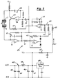
- Figure 2 is a circuit diagram of an AGC controlled drive circuit for use in the embodiment of Figure 1.
- the invention is illustrated in connection with a rotation rate sensor of a type which is sometimes referred to as a "quartz rate sensor".
- a rotation rate sensor of a type which is sometimes referred to as a "quartz rate sensor”.
- accelerometers other types of rate sensors, and other types of transducers from which a ratiometric output is desired.
- the rate sensor illustrated in Figure 1 is in many respects similar to a rate sensor shown in copending U.S. application Serial No. 08/100,759, Filed August 2, 1993. It has a double ended tuning fork 11 fabricated of a piezoelectric material such as quartz.
- the tuning fork has a pair of drive tines 12 and a pair of pickup tines 13 extending in opposite directions from a central body or base 14, with drive electrodes 16, 17 and pickup electrodes 18, 19 on the tines for coupling signals to and from the piezoelectric structure.
- drive electrodes 16, 17 and pickup electrodes 18, 19 on the tines for coupling signals to and from the piezoelectric structure.
- FIG 1 For ease of illustration, only two drive electrodes and two pickup electrodes are shown in Figure 1, and they are shown schematically. In an actual tuning fork, however, a greater number of electrodes is generally employed, and in the example illustrated in U.S. Serial No. 08/100,759, two pairs of drive electrodes and two pairs of pickup electrodes are employed.
- a drive circuit 21 is connected to the drive electrodes, and a pickup circuit 22 is connected to the pickup electrodes.
- a pickup circuit 22 is connected to the pickup electrodes.
- the drive circuit is an oscillator with automatic gain control (AGC) which comprises a current amplifier 26 and an AGC loop 27.
- the AGC loop includes an AGC amplifier 28, a level detector 29 and a loop amplifier/filter 31.
- the input of current amplifier 26 is connected to "drive low" electrode 16
- the output of the current amplifier is connected to the input of the AGC amplifier 28, and the output of the AGC amplifier is connected to "drive high” electrode 17.
- the signal at the output of current amplifier 26 is a sine wave.
- Level detector 29 converts the peak of the sine wave amplitude to an equivalent RMS value, and the output of the level detector is compared to a reference current.
- the error or difference between the reference and the output of the level detector is amplified by loop filter/amplifier 31 and applied to the control input of AGC amplifier 28 to control the gain of the AGC amplifier.
- the pickup circuit is illustrated as including a charge amplifier 33, a synchronous demodulator 34, and a low pass filter 36.
- "Pickup low" electrode 18 is connected to one input of the charge amplifier through a relatively small (e.g., 100 ohm) resistor 37, and "pickup high” electrode 19 is connected to a second input of the charge amplifier.
- the signal from the charge amplifier is demodulated in accordance with the signal from current amplifier 26 in the drive circuit, and after filtering to remove high frequency components, the demodulated signal is delivered to an output terminal 39.
- the system shown in Figure 1 and in U.S. Serial No. 08/100,759 also includes a test circuit 40 which permits an attenuated signal from the drive circuit to be applied to the input of the pickup circuit through resistor 37 for testing of the system.
- the test circuit includes a normally open switch 41 and an attenuator 42 connected in series between the output of current amplifier 26 and the input side of resistor 37.
- the present embodiment differs from the system disclosed in U.S. Serial No. 08/100,759 in that supply voltage (V cc ) is now used as a reference voltage for the AGC circuit, so that the system has a ratiometric output wherein both the drive signal and the output signal are linearly proportional to the supply voltage.
- V cc supply voltage
- the scale of the system now moves up and down with the supply voltage, and there is no need for dead zones at the ends of the scale.
- a user can use his own A/D converter with its own power supply as the reference voltage, and the A/D converter will read out a "pure rate" in digital format regardless of the supply voltage. This represents a substantial improvement over systems such as the one shown in U.S. Serial No. 08/100,759 where the reference for AGC circuit is a fixed voltage.
- the system has a power supply 43 which provides the operating voltage V cc for drive and pickup circuits.
- the power supply includes a filter consisting of capacitors 44-47 and a choke 48, with the voltage V cc being taken from the output side of the choke.
- a voltage regulator 49 provides a regulated voltage for other portions of the system.
- the AGC controlled drive circuit includes a current amplifier 51, a full-wave rectifier 52, an integrator 53 and a comparator/multiplier 54, the latter comprising an amplifier 56 and a transistor 57 having its base connected to the output of the amplifier.
- a summing node 58 is provided at the input of the integrator.
- the "drive low” electrode 16 on the tuning fork is connected to the input of current amplifier 51, and the output of the current amplifier is connected to the input of comparator amplifier 56 through a coupling capacitor 59.
- the output of the comparator/multiplier, taken at the collector of transistor 57 is connected to the "drive high" electrode 17 on the tuning fork.
- Current from current amplifier 51 is also rectified and applied to summing node 58 as a full-wave rectified negative current.
- a first resistor 60 is connected between the output of the current amplifier and the summing node 58
- a second resistor 61 is connected between the output of the current amplifier and the input of a half-wave rectifier 62.
- a resistor 63 is connected between the output of the half-wave rectifier and the summing node.
- the current through resistor 60 is a sine wave
- the current through resistor 62 is a negative going half-wave rectified sine wave.
- the amplitude of the current through resistor 60 is one half the amplitude of the current through resistor 62, and these two currents add together to produce a negative full-wave rectified current having the same amplitude as the half-wave rectified current.
- the output of integrator 53 is connected to the emitter of multiplier transistor 57 by a resistor 64 to control the level of the drive signal.
- a reference current I REF proportional to the supply voltage V cc is applied to the summing node through resistors 65, 66 for combination with the currents from the full-wave rectifier.
- a drive voltage is applied to "drive high" electrode 17 by comparator/multiplier 54, with the level of the drive voltage being controlled by the output of integrator 53.
- Current from the "drive low” electrode 17 is amplified by current amplifier 51 to provide a voltage of sinusoidal waveform which is proportional to the drive current.
- This voltage is rectified by full-wave rectifier 52 to provide an inverted or negative current which is applied to the summing node through resistors 60, 63.
- the reference current I REF which is supplied to the node through resistor 66 and is proportional to the supply voltage V cc .
- the net current into the summing node and integrator is zero. That condition is met when the negative net current from the full-wave rectifier is equal to the reference current.
- the comparator/multiplier converts the sinusoidal voltage from current amplifier 51 to a square wave, with an amplitude controlled by output of the integrator. That output is, to a large extent, dependent upon the supply voltage, and the drive current applied to the tuning fork is thus proportional to the supply voltage.
- the current coupled to the pickup circuit corresponds closely to the drive current, and with the supply voltage providing the reference for the AGC circuit, the output voltage from the pickup circuit is linearly proportional to the supply voltage.
- the AGC action will oppose the change and return the drive current to its preset level by altering the drive voltage appropriately. If, for example, the drive current should start to increase, the current supplied to the summing node from the full-wave rectifier will start to increase, resulting in a net negative current into the summing node. This results in an increase in voltage at the output of the integrator, thus reducing the drive current control voltage, and hence the drive current itself, until the net current into the summing node at the integrator returns to zero. If however, the supply voltage should change, the reference current I REF will change in proportion to it, and the output of the integrator will follow that change.
- the drive voltage applied to the tuning fork will change accordingly, and the drive current will remain proportional to the supply voltage.
- the currents supplied to the summing node by full-wave rectifier 52 will adjust to maintain a zero net current into the integrator with the new level of reference current.
- rate sensor having a tuning fork fabricated of piezoelectric or quartz material
- it is equally applicable to other types of transducers and other types of vibratory elements. It could, for example, be utilized in a rate sensor or other transducer having a vibratory silicon sensor which is electrostatically actuated and capacitively sensed.
- the described embodiment has a number of important features and advantages.
- the system has a ratiometric output, with both the drive current and the output signal being linearly proportional to the supply voltage.
- the scale of the system moves up and down with the supply voltage, and there is no need for dead zones at the ends of the scale.
- a user can use his own A/D converter with its power supply voltage as a reference voltage, and the A/D converter will read out in pure rate in digital format regardless of the supply voltage.
Landscapes
- Engineering & Computer Science (AREA)
- Signal Processing (AREA)
- Physics & Mathematics (AREA)
- General Physics & Mathematics (AREA)
- Radar, Positioning & Navigation (AREA)
- Remote Sensing (AREA)
- Gyroscopes (AREA)
Abstract
Description
- This invention pertains generally to transducers such as rotation rate sensors and inertial sensors and, more particularly, to a transducer system and method in which the output voltage is linearly proportional to the power supply voltage.
- Transducers such as rotation rate sensors, accelerometers and other inertial sensors are used in a wide variety of applications such as control systems employed in aircraft, automobiles and other vehicles. One early type of accelerometer had a potentiometer with an adjustable element or wiper driven by a proofmass to vary the resistance of the potentiometer. That type of accelerometer was a ratiometric device in that the output voltage was linearly proportional to the supply voltage as long as the potentiometer itself was linear.
- More recently, accelerometers, rate sensors and other transducers have employed vibrating quartz sensing elements which are substantially more sensitive than potentiometric devices. Unfortunately, however, up to now it has not been possible to obtain a ratiometric output from a vibrating quartz device.
- It is in general therefore desirable to provide a new and improved transducer and method.
- It is also desirable to provide a transducer and method of the above character which overcome limitations and disadvantages of the prior art.
- These and other objects are achieved in preferred embodiments of the invention by providing a ratiometric transducer and method in which the output signal is linearly proportional to the supply voltage or level of excitation. A drive circuit applies a drive signal to an element which undergoes a change in accordance with a condition to be monitored (e.g., rotation or acceleration), and a pickup circuit receives signals from the element and provides an output signal corresponding to the condition to be monitored. Operating voltage is supplied to the drive circuit from a power supply, and the gain of the drive circuit is adjusted in accordance with variations in the operating voltage to make the drive signal and the output signal proportional to the operating voltage.
- Figure 1 is a block diagram of one embodiment of a ratiometric transducer incorporating the invention.
- Figure 2 is a circuit diagram of an AGC controlled drive circuit for use in the embodiment of Figure 1.
- In the drawings, the invention is illustrated in connection with a rotation rate sensor of a type which is sometimes referred to as a "quartz rate sensor". However, it is equally applicable to accelerometers, other types of rate sensors, and other types of transducers from which a ratiometric output is desired.
The rate sensor illustrated in Figure 1 is in many respects similar to a rate sensor shown in copending U.S. application Serial No. 08/100,759, Filed August 2, 1993. It has a double endedtuning fork 11 fabricated of a piezoelectric material such as quartz. The tuning fork has a pair ofdrive tines 12 and a pair ofpickup tines 13 extending in opposite directions from a central body orbase 14, withdrive electrodes pickup electrodes - A
drive circuit 21 is connected to the drive electrodes, and apickup circuit 22 is connected to the pickup electrodes. When the tuning fork is rotated about itslongitudinal axis 23, Coriolis forces having a frequency corresponding to the rate of rotation produce a torsioning of the drive tines. That torsioning is transmitted through the piezoelectric structure to the pickup tines, and the signal coupled to the pickup electrodes varies in amplitude at the drive frequency in accordance with the rate of rotation. - The drive circuit is an oscillator with automatic gain control (AGC) which comprises a
current amplifier 26 and anAGC loop 27. The AGC loop includes anAGC amplifier 28, alevel detector 29 and a loop amplifier/filter 31. The input ofcurrent amplifier 26 is connected to "drive low"electrode 16, the output of the current amplifier is connected to the input of theAGC amplifier 28, and the output of the AGC amplifier is connected to "drive high"electrode 17. The signal at the output ofcurrent amplifier 26 is a sine wave.Level detector 29 converts the peak of the sine wave amplitude to an equivalent RMS value, and the output of the level detector is compared to a reference current. The error or difference between the reference and the output of the level detector is amplified by loop filter/amplifier 31 and applied to the control input ofAGC amplifier 28 to control the gain of the AGC amplifier. - The pickup circuit is illustrated as including a
charge amplifier 33, asynchronous demodulator 34, and alow pass filter 36. "Pickup low"electrode 18 is connected to one input of the charge amplifier through a relatively small (e.g., 100 ohm)resistor 37, and "pickup high"electrode 19 is connected to a second input of the charge amplifier. The signal from the charge amplifier is demodulated in accordance with the signal fromcurrent amplifier 26 in the drive circuit, and after filtering to remove high frequency components, the demodulated signal is delivered to anoutput terminal 39. - The system shown in Figure 1 and in U.S. Serial No. 08/100,759 also includes a
test circuit 40 which permits an attenuated signal from the drive circuit to be applied to the input of the pickup circuit throughresistor 37 for testing of the system. The test circuit includes a normallyopen switch 41 and anattenuator 42 connected in series between the output ofcurrent amplifier 26 and the input side ofresistor 37. - The present embodiment differs from the system disclosed in U.S. Serial No. 08/100,759 in that supply voltage (Vcc) is now used as a reference voltage for the AGC circuit, so that the system has a ratiometric output wherein both the drive signal and the output signal are linearly proportional to the supply voltage. The scale of the system now moves up and down with the supply voltage, and there is no need for dead zones at the ends of the scale. A user can use his own A/D converter with its own power supply as the reference voltage, and the A/D converter will read out a "pure rate" in digital format regardless of the supply voltage. This represents a substantial improvement over systems such as the one shown in U.S. Serial No. 08/100,759 where the reference for AGC circuit is a fixed voltage.
- As illustrated in Figure 2, the system has a
power supply 43 which provides the operating voltage Vcc for drive and pickup circuits. The power supply includes a filter consisting of capacitors 44-47 and a choke 48, with the voltage Vcc being taken from the output side of the choke. Avoltage regulator 49 provides a regulated voltage for other portions of the system. - In this embodiment, the AGC controlled drive circuit includes a
current amplifier 51, a full-wave rectifier 52, anintegrator 53 and a comparator/multiplier 54, the latter comprising anamplifier 56 and atransistor 57 having its base connected to the output of the amplifier. Asumming node 58 is provided at the input of the integrator. - The "drive low"
electrode 16 on the tuning fork is connected to the input ofcurrent amplifier 51, and the output of the current amplifier is connected to the input ofcomparator amplifier 56 through acoupling capacitor 59. The output of the comparator/multiplier, taken at the collector oftransistor 57 is connected to the "drive high"electrode 17 on the tuning fork. - Current from
current amplifier 51 is also rectified and applied to summingnode 58 as a full-wave rectified negative current. In this regard, afirst resistor 60 is connected between the output of the current amplifier and thesumming node 58, and asecond resistor 61 is connected between the output of the current amplifier and the input of a half-wave rectifier 62. Aresistor 63 is connected between the output of the half-wave rectifier and the summing node. The current throughresistor 60 is a sine wave, and the current throughresistor 62 is a negative going half-wave rectified sine wave. By makingresistor 60 twice the value ofresistor 62, the amplitude of the current throughresistor 60 is one half the amplitude of the current throughresistor 62, and these two currents add together to produce a negative full-wave rectified current having the same amplitude as the half-wave rectified current. The output ofintegrator 53 is connected to the emitter ofmultiplier transistor 57 by a resistor 64 to control the level of the drive signal. - A reference current IREF proportional to the supply voltage Vcc is applied to the summing node through
resistors resistor 66 to a Zener diode or other constant voltage source. - Operation and use of the embodiment of Figure 2 are as follows. A drive voltage is applied to "drive high"
electrode 17 by comparator/multiplier 54, with the level of the drive voltage being controlled by the output ofintegrator 53. Current from the "drive low"electrode 17 is amplified bycurrent amplifier 51 to provide a voltage of sinusoidal waveform which is proportional to the drive current. This voltage is rectified by full-wave rectifier 52 to provide an inverted or negative current which is applied to the summing node throughresistors resistor 66 and is proportional to the supply voltage Vcc. At the stable operating point, the net current into the summing node and integrator is zero. That condition is met when the negative net current from the full-wave rectifier is equal to the reference current. - The comparator/multiplier converts the sinusoidal voltage from
current amplifier 51 to a square wave, with an amplitude controlled by output of the integrator. That output is, to a large extent, dependent upon the supply voltage, and the drive current applied to the tuning fork is thus proportional to the supply voltage. The current coupled to the pickup circuit corresponds closely to the drive current, and with the supply voltage providing the reference for the AGC circuit, the output voltage from the pickup circuit is linearly proportional to the supply voltage. - In the event that the drive current should start to drift due to something other than a change in the supply voltage, the AGC action will oppose the change and return the drive current to its preset level by altering the drive voltage appropriately. If, for example, the drive current should start to increase, the current supplied to the summing node from the full-wave rectifier will start to increase, resulting in a net negative current into the summing node. This results in an increase in voltage at the output of the integrator, thus reducing the drive current control voltage, and hence the drive current itself, until the net current into the summing node at the integrator returns to zero. If however, the supply voltage should change, the reference current IREF will change in proportion to it, and the output of the integrator will follow that change. The drive voltage applied to the tuning fork will change accordingly, and the drive current will remain proportional to the supply voltage. The currents supplied to the summing node by full-
wave rectifier 52 will adjust to maintain a zero net current into the integrator with the new level of reference current. - Although the invention has been described with specific reference to a rate sensor having a tuning fork fabricated of piezoelectric or quartz material, it is equally applicable to other types of transducers and other types of vibratory elements. It could, for example, be utilized in a rate sensor or other transducer having a vibratory silicon sensor which is electrostatically actuated and capacitively sensed.
- The described embodiment has a number of important features and advantages. The system has a ratiometric output, with both the drive current and the output signal being linearly proportional to the supply voltage. The scale of the system moves up and down with the supply voltage, and there is no need for dead zones at the ends of the scale. A user can use his own A/D converter with its power supply voltage as a reference voltage, and the A/D converter will read out in pure rate in digital format regardless of the supply voltage.
- It is apparent from the foregoing that a new and improved ratiometric transducer and method have been provided. While only certain presently preferred embodiments have been described in detail, as will be apparent to those familiar with the art, certain changes and modifications can be made without departing from the scope of the invention as defined by the following claims.
Claims (10)
- In an inertial transducer: a vibratory element, a drive circuit for applying a drive signal to the vibratory element, a pickup circuit coupled to the vibratory element for providing an output signal corresponding to movement of the vibratory element, a power supply for supplying operating power to the drive circuit, and means responsive to the power supply voltage for controlling the drive level so that the drive signal and the output signal are proportional to the supply voltage.
- The transducer of Claim 1 wherein the means for controlling the drive level comprises an automatic gain control (AGC) circuit, and the supply voltage is applied to a control element of the AGC circuit.
- In a transducer: means including a pickup circuit responsive to a condition to be monitored for providing an output signal corresponding to that condition, a drive circuit for providing a drive signal which stimulates a response in the pickup circuit which varies in accordance with the condition to be monitored, a power supply for supplying operating power to the drive circuit, and means responsive to the power supply voltage for controlling the drive level so that drive signal and the output signal are proportional to the supply voltage.
- The transducer of Claim 3 wherein the means for controlling the drive level comprises an automatic gain control (AGC) circuit, and the supply voltage is applied to a control element of the AGC circuit.
- In a transducer for monitoring rotation: a tuning fork, a drive circuit coupled to the tuning fork for applying a drive signal to the tuning fork to cause vibration of the tuning fork, a pickup circuit responsive to signals produced by vibration of the tuning fork for providing an output signal corresponding to rotation of the tuning fork, a power supply for supplying operating voltage to the drive circuit, an automatic gain control in the drive circuit for controlling the level of the drive signal, and means for applying the operating voltage to the gain control as a control signal to make the level of the drive signal and the output signal proportional to the operating voltage.
- In a method of monitoring inertial activity, the steps of: applying a drive signal from a drive circuit to a vibratory element which is subjected to an inertial force, monitoring signals from the vibratory element with a pickup circuit to provide an output signal corresponding to the inertial force, supplying operating voltage to the drive circuit from a power supply, and controlling the drive circuit in accordance with the operating voltage so that the drive signal and the output signal are proportional to the operating voltage.
- The method of Claim 6 wherein the drive circuit is controlled by controlling the gain of the drive circuit in accordance with the operating voltage.
- In a method of providing an output signal which is proportional to level of excitation, the steps of: monitoring a condition with a pickup circuit to provide an output signal corresponding to the condition, operating a drive circuit to provide a drive signal which stimulates a response in the pickup circuit which varies in accordance with the condition to be monitored, supplying an operating voltage from a power supply to the drive circuit, and controlling the drive circuit in accordance with the operating voltage so that the drive signal and the output signal are proportional to the operating voltage.
- The method of Claim 8 wherein the drive circuit is controlled by controlling the gain of the drive circuit in accordance with the operating voltage.
- In a method of monitoring rotation, the steps of: applying a drive signal from a drive circuit to a tuning fork to cause vibration of the tuning fork, monitoring signals produced by vibration of the tuning fork with a pickup circuit to provide an output signal corresponding to rotation of the tuning fork, supplying an operating voltage to the drive circuit, and adjusting gain in the drive circuit in response to changes in the operating voltage to make the level of the drive signal and the output signal proportional to the operating voltage.
Applications Claiming Priority (2)
| Application Number | Priority Date | Filing Date | Title |
|---|---|---|---|
| US08/306,766 US5942686A (en) | 1994-09-15 | 1994-09-15 | Ratiometric transducer and method |
| US306766 | 1994-09-15 |
Publications (2)
| Publication Number | Publication Date |
|---|---|
| EP0702207A1 true EP0702207A1 (en) | 1996-03-20 |
| EP0702207B1 EP0702207B1 (en) | 1999-09-29 |
Family
ID=23186743
Family Applications (1)
| Application Number | Title | Priority Date | Filing Date |
|---|---|---|---|
| EP95305489A Expired - Lifetime EP0702207B1 (en) | 1994-09-15 | 1995-08-07 | Ratiometric transducer and method |
Country Status (4)
| Country | Link |
|---|---|
| US (1) | US5942686A (en) |
| EP (1) | EP0702207B1 (en) |
| JP (1) | JP2781161B2 (en) |
| DE (1) | DE69512492T2 (en) |
Cited By (4)
| Publication number | Priority date | Publication date | Assignee | Title |
|---|---|---|---|---|
| DE10240087A1 (en) * | 2002-08-30 | 2004-03-11 | Austriamicrosystems Ag | vibration gyro |
| US6705151B2 (en) | 1995-05-30 | 2004-03-16 | Matsushita Electric Industrial Co., Ltd. | Angular velocity sensor |
| EP2037218A2 (en) | 2007-09-11 | 2009-03-18 | EM Microelectronic-Marin SA | Electronic circuit for measuring a physical parameter supplying an analogue measurement signal depending on the input voltage |
| WO2011073891A1 (en) * | 2009-12-14 | 2011-06-23 | Rafael -Advanced Defense Systems Ltd. | Adaptive modifications in micro opto - electro -mechanical systems |
Families Citing this family (19)
| Publication number | Priority date | Publication date | Assignee | Title |
|---|---|---|---|---|
| US6912901B1 (en) | 1995-05-30 | 2005-07-05 | Matsushita Electric Industrial Co., Ltd. | Angular velocity sensor |
| JP3932661B2 (en) * | 1998-03-31 | 2007-06-20 | 松下電器産業株式会社 | Angular velocity sensor drive circuit |
| US6359578B1 (en) * | 2000-02-04 | 2002-03-19 | Delphi Technologies | System for externally referenced ratiometric signal processing |
| US6497146B1 (en) | 2000-09-15 | 2002-12-24 | Bei Technologies, Inc. | Inertial rate sensor and method with built-in testing |
| US6510737B1 (en) | 2000-09-15 | 2003-01-28 | Bei Technologies, Inc. | Inertial rate sensor and method with improved tuning fork drive |
| US6553835B1 (en) | 2000-09-15 | 2003-04-29 | Bei Technologies, Inc. | Inertial rate sensor and method with improved clocking |
| JP4668407B2 (en) * | 2000-12-08 | 2011-04-13 | 京セラキンセキ株式会社 | Angular velocity sensor |
| JP4697373B2 (en) * | 2001-08-14 | 2011-06-08 | セイコーエプソン株式会社 | Physical quantity measuring method, physical quantity measuring device, and method of supplying power to physical quantity measuring instrument |
| US6789029B2 (en) * | 2002-10-18 | 2004-09-07 | Motorola, Inc. | Method and apparatus for signal extraction in an electronic sensor |
| US6934665B2 (en) * | 2003-10-22 | 2005-08-23 | Motorola, Inc. | Electronic sensor with signal conditioning |
| JP3964875B2 (en) | 2004-02-16 | 2007-08-22 | 株式会社ジャイトロニクス | Angular velocity sensor |
| US7464590B1 (en) * | 2004-03-12 | 2008-12-16 | Thomson Licensing | Digitally programmable bandwidth for vibratory rate gyroscope |
| DE102004029941B3 (en) * | 2004-06-21 | 2005-12-15 | Infineon Technologies Ag | System for evaluating a sensor signal |
| JP2006105659A (en) * | 2004-10-01 | 2006-04-20 | Nec Tokin Corp | Piezoelectric vibration gyro, and sensitivity regulation method therefor |
| JP4534741B2 (en) * | 2004-12-10 | 2010-09-01 | 株式会社デンソー | Gyro sensor |
| US7779688B2 (en) * | 2006-12-20 | 2010-08-24 | Epson Toyocom Corporation | Vibration gyro sensor |
| JP2008209182A (en) * | 2007-02-26 | 2008-09-11 | Seiko Epson Corp | Detection device, sensor and electronic device |
| JP5162206B2 (en) * | 2007-11-12 | 2013-03-13 | セイコーインスツル株式会社 | Oscillator, oscillator manufacturing method, and oscillator |
| RU175143U1 (en) * | 2017-01-31 | 2017-11-23 | Акционерное общество "Вибро-прибор" | Piezoelectric vibration velocity transducer |
Citations (2)
| Publication number | Priority date | Publication date | Assignee | Title |
|---|---|---|---|---|
| EP0517259A2 (en) * | 1991-06-07 | 1992-12-09 | Akai Electric Co., Ltd. | Vibration control apparatus |
| EP0584798A1 (en) * | 1992-08-27 | 1994-03-02 | Murata Manufacturing Co., Ltd. | Driving circuit for gyroscope |
Family Cites Families (7)
| Publication number | Priority date | Publication date | Assignee | Title |
|---|---|---|---|---|
| US4674331A (en) * | 1984-07-27 | 1987-06-23 | Watson Industries Inc. | Angular rate sensor |
| US4884446A (en) * | 1987-03-12 | 1989-12-05 | Ljung Per B | Solid state vibrating gyro |
| US4930351A (en) * | 1988-03-24 | 1990-06-05 | Wjm Corporation | Vibratory linear acceleration and angular rate sensing system |
| US5014554A (en) * | 1989-04-14 | 1991-05-14 | Matsushita Electric Industrial Co., Ltd. | Angular rate sensor |
| JPH04216409A (en) * | 1990-12-18 | 1992-08-06 | Matsushita Electric Ind Co Ltd | angular velocity sensor |
| EP0503807B1 (en) * | 1991-03-12 | 1996-09-25 | New Sd, Inc. | Single ended tuning fork inertial sensor and method |
| US5426970A (en) * | 1993-08-02 | 1995-06-27 | New Sd, Inc. | Rotation rate sensor with built in test circuit |
-
1994
- 1994-09-15 US US08/306,766 patent/US5942686A/en not_active Expired - Fee Related
-
1995
- 1995-08-07 DE DE69512492T patent/DE69512492T2/en not_active Expired - Fee Related
- 1995-08-07 EP EP95305489A patent/EP0702207B1/en not_active Expired - Lifetime
- 1995-08-28 JP JP7219149A patent/JP2781161B2/en not_active Expired - Fee Related
Patent Citations (2)
| Publication number | Priority date | Publication date | Assignee | Title |
|---|---|---|---|---|
| EP0517259A2 (en) * | 1991-06-07 | 1992-12-09 | Akai Electric Co., Ltd. | Vibration control apparatus |
| EP0584798A1 (en) * | 1992-08-27 | 1994-03-02 | Murata Manufacturing Co., Ltd. | Driving circuit for gyroscope |
Cited By (7)
| Publication number | Priority date | Publication date | Assignee | Title |
|---|---|---|---|---|
| US6705151B2 (en) | 1995-05-30 | 2004-03-16 | Matsushita Electric Industrial Co., Ltd. | Angular velocity sensor |
| DE10240087A1 (en) * | 2002-08-30 | 2004-03-11 | Austriamicrosystems Ag | vibration gyro |
| DE10240087B4 (en) * | 2002-08-30 | 2005-06-16 | Austriamicrosystems Ag | vibration gyro |
| DE10240087C5 (en) * | 2002-08-30 | 2011-12-01 | Austriamicrosystems Ag | vibration gyro |
| EP2037218A2 (en) | 2007-09-11 | 2009-03-18 | EM Microelectronic-Marin SA | Electronic circuit for measuring a physical parameter supplying an analogue measurement signal depending on the input voltage |
| US8051711B2 (en) | 2007-09-11 | 2011-11-08 | Em Microelectronic-Marin S.A. | Electronic circuit for measuring a physical parameter supplying an analogue measurement signal dependent upon the supply voltage |
| WO2011073891A1 (en) * | 2009-12-14 | 2011-06-23 | Rafael -Advanced Defense Systems Ltd. | Adaptive modifications in micro opto - electro -mechanical systems |
Also Published As
| Publication number | Publication date |
|---|---|
| DE69512492D1 (en) | 1999-11-04 |
| JPH08178945A (en) | 1996-07-12 |
| US5942686A (en) | 1999-08-24 |
| EP0702207B1 (en) | 1999-09-29 |
| JP2781161B2 (en) | 1998-07-30 |
| DE69512492T2 (en) | 2000-01-05 |
Similar Documents
| Publication | Publication Date | Title |
|---|---|---|
| EP0702207B1 (en) | Ratiometric transducer and method | |
| US4642555A (en) | Differential capacitance detector | |
| US4584885A (en) | Capacitive detector for transducers | |
| US4302728A (en) | Ultrasonic wave oscillator circuit with output meter | |
| US7107841B2 (en) | Capacitance-sensing vibratory gyro and method for detecting change in capacitance | |
| JPH0792486B2 (en) | Electrostatic capacity monitor-device | |
| US4767520A (en) | Device for detecting air-fuel ratio of engine | |
| US6407631B2 (en) | Charge-type sensor amplifying circuit | |
| US5902931A (en) | Vibration gyroscope | |
| EP0216288B1 (en) | Interface circuit between a sensor, particularly a thick film pressure sensor, and an electrodynamic instrument, and a sensor incorporating such a circuit | |
| JP2000002543A (en) | Angular velocity sensor | |
| KR100210334B1 (en) | Vibration gyroscope and method for adjusting vibration-gyroscope characteristics | |
| JPH0155419B2 (en) | ||
| JP3341363B2 (en) | Humidity detector | |
| JPH06148231A (en) | Yaw rate sensor temperature compensation method and temperature compensation device | |
| JPS61142415A (en) | Angular velocity detector | |
| JPH0519796Y2 (en) | ||
| SU1644046A1 (en) | In telligence parameter-to-freqiency converter | |
| JP2527604Y2 (en) | Integrator integration time constant switch connected to detector | |
| JPS6175251A (en) | Water drop detection sensor | |
| JPH0327472B2 (en) | ||
| Huijsing et al. | Two-wire ratio-frequency converter | |
| JPH0850069A (en) | Capacitive pressure sensor | |
| JPS60222733A (en) | Method and apparatus for detecting force | |
| JPH0831823B2 (en) | Optical reception level monitor circuit |
Legal Events
| Date | Code | Title | Description |
|---|---|---|---|
| PUAI | Public reference made under article 153(3) epc to a published international application that has entered the european phase |
Free format text: ORIGINAL CODE: 0009012 |
|
| AK | Designated contracting states |
Kind code of ref document: A1 Designated state(s): CH DE FR GB IT LI SE |
|
| 17P | Request for examination filed |
Effective date: 19960305 |
|
| 17Q | First examination report despatched |
Effective date: 19971205 |
|
| GRAG | Despatch of communication of intention to grant |
Free format text: ORIGINAL CODE: EPIDOS AGRA |
|
| GRAG | Despatch of communication of intention to grant |
Free format text: ORIGINAL CODE: EPIDOS AGRA |
|
| GRAH | Despatch of communication of intention to grant a patent |
Free format text: ORIGINAL CODE: EPIDOS IGRA |
|
| GRAH | Despatch of communication of intention to grant a patent |
Free format text: ORIGINAL CODE: EPIDOS IGRA |
|
| GRAA | (expected) grant |
Free format text: ORIGINAL CODE: 0009210 |
|
| AK | Designated contracting states |
Kind code of ref document: B1 Designated state(s): CH DE FR GB IT LI SE |
|
| REG | Reference to a national code |
Ref country code: CH Ref legal event code: NV Representative=s name: BOVARD AG PATENTANWAELTE Ref country code: CH Ref legal event code: EP |
|
| REF | Corresponds to: |
Ref document number: 69512492 Country of ref document: DE Date of ref document: 19991104 |
|
| ET | Fr: translation filed | ||
| ITF | It: translation for a ep patent filed | ||
| PLBQ | Unpublished change to opponent data |
Free format text: ORIGINAL CODE: EPIDOS OPPO |
|
| PLBI | Opposition filed |
Free format text: ORIGINAL CODE: 0009260 |
|
| PLBF | Reply of patent proprietor to notice(s) of opposition |
Free format text: ORIGINAL CODE: EPIDOS OBSO |
|
| 26 | Opposition filed |
Opponent name: TEMIC TELEFUNKEN MICROELECTRONIC GMBH Effective date: 20000629 |
|
| PLBF | Reply of patent proprietor to notice(s) of opposition |
Free format text: ORIGINAL CODE: EPIDOS OBSO |
|
| PLBF | Reply of patent proprietor to notice(s) of opposition |
Free format text: ORIGINAL CODE: EPIDOS OBSO |
|
| REG | Reference to a national code |
Ref country code: GB Ref legal event code: IF02 |
|
| PLBO | Opposition rejected |
Free format text: ORIGINAL CODE: EPIDOS REJO |
|
| APAC | Appeal dossier modified |
Free format text: ORIGINAL CODE: EPIDOS NOAPO |
|
| PLAB | Opposition data, opponent's data or that of the opponent's representative modified |
Free format text: ORIGINAL CODE: 0009299OPPO |
|
| R26 | Opposition filed (corrected) |
Opponent name: CONTI TEMIC MICROELECTRONIC GMBH Effective date: 20000629 |
|
| APAC | Appeal dossier modified |
Free format text: ORIGINAL CODE: EPIDOS NOAPO |
|
| PLBN | Opposition rejected |
Free format text: ORIGINAL CODE: 0009273 |
|
| STAA | Information on the status of an ep patent application or granted ep patent |
Free format text: STATUS: OPPOSITION REJECTED |
|
| 27O | Opposition rejected |
Effective date: 20020401 |
|
| APAA | Appeal reference recorded |
Free format text: ORIGINAL CODE: EPIDOS REFN |
|
| APAH | Appeal reference modified |
Free format text: ORIGINAL CODE: EPIDOSCREFNO |
|
| PGFP | Annual fee paid to national office [announced via postgrant information from national office to epo] |
Ref country code: SE Payment date: 20070817 Year of fee payment: 13 Ref country code: IT Payment date: 20070828 Year of fee payment: 13 |
|
| PGFP | Annual fee paid to national office [announced via postgrant information from national office to epo] |
Ref country code: DE Payment date: 20080909 Year of fee payment: 14 Ref country code: CH Payment date: 20080901 Year of fee payment: 14 |
|
| PGFP | Annual fee paid to national office [announced via postgrant information from national office to epo] |
Ref country code: FR Payment date: 20080822 Year of fee payment: 14 |
|
| PGFP | Annual fee paid to national office [announced via postgrant information from national office to epo] |
Ref country code: GB Payment date: 20080827 Year of fee payment: 14 |
|
| EUG | Se: european patent has lapsed | ||
| PG25 | Lapsed in a contracting state [announced via postgrant information from national office to epo] |
Ref country code: IT Free format text: LAPSE BECAUSE OF NON-PAYMENT OF DUE FEES Effective date: 20080807 |
|
| REG | Reference to a national code |
Ref country code: CH Ref legal event code: PL |
|
| GBPC | Gb: european patent ceased through non-payment of renewal fee |
Effective date: 20090807 |
|
| PG25 | Lapsed in a contracting state [announced via postgrant information from national office to epo] |
Ref country code: LI Free format text: LAPSE BECAUSE OF NON-PAYMENT OF DUE FEES Effective date: 20090831 Ref country code: CH Free format text: LAPSE BECAUSE OF NON-PAYMENT OF DUE FEES Effective date: 20090831 |
|
| REG | Reference to a national code |
Ref country code: FR Ref legal event code: ST Effective date: 20100430 |
|
| PG25 | Lapsed in a contracting state [announced via postgrant information from national office to epo] |
Ref country code: SE Free format text: LAPSE BECAUSE OF NON-PAYMENT OF DUE FEES Effective date: 20080808 Ref country code: FR Free format text: LAPSE BECAUSE OF NON-PAYMENT OF DUE FEES Effective date: 20090831 Ref country code: DE Free format text: LAPSE BECAUSE OF NON-PAYMENT OF DUE FEES Effective date: 20100302 |
|
| PG25 | Lapsed in a contracting state [announced via postgrant information from national office to epo] |
Ref country code: GB Free format text: LAPSE BECAUSE OF NON-PAYMENT OF DUE FEES Effective date: 20090807 |