EP0696860B1 - Optical time compression multiplexing transmission system - Google Patents
Optical time compression multiplexing transmission system Download PDFInfo
- Publication number
- EP0696860B1 EP0696860B1 EP95401877A EP95401877A EP0696860B1 EP 0696860 B1 EP0696860 B1 EP 0696860B1 EP 95401877 A EP95401877 A EP 95401877A EP 95401877 A EP95401877 A EP 95401877A EP 0696860 B1 EP0696860 B1 EP 0696860B1
- Authority
- EP
- European Patent Office
- Prior art keywords
- optical
- signal
- received
- equipment
- point
- Prior art date
- Legal status (The legal status is an assumption and is not a legal conclusion. Google has not performed a legal analysis and makes no representation as to the accuracy of the status listed.)
- Expired - Lifetime
Links
Images


Classifications
-
- H—ELECTRICITY
- H04—ELECTRIC COMMUNICATION TECHNIQUE
- H04L—TRANSMISSION OF DIGITAL INFORMATION, e.g. TELEGRAPHIC COMMUNICATION
- H04L5/00—Arrangements affording multiple use of the transmission path
- H04L5/14—Two-way operation using the same type of signal, i.e. duplex
- H04L5/1461—Suppression of signals in the return path, i.e. bidirectional control circuits
-
- H—ELECTRICITY
- H04—ELECTRIC COMMUNICATION TECHNIQUE
- H04J—MULTIPLEX COMMUNICATION
- H04J14/00—Optical multiplex systems
- H04J14/08—Time-division multiplex systems
-
- H—ELECTRICITY
- H04—ELECTRIC COMMUNICATION TECHNIQUE
- H04J—MULTIPLEX COMMUNICATION
- H04J3/00—Time-division multiplex systems
- H04J3/02—Details
- H04J3/06—Synchronising arrangements
- H04J3/0602—Systems characterised by the synchronising information used
- H04J3/0605—Special codes used as synchronising signal
- H04J3/0608—Detectors therefor, e.g. correlators, state machines
-
- H—ELECTRICITY
- H04—ELECTRIC COMMUNICATION TECHNIQUE
- H04L—TRANSMISSION OF DIGITAL INFORMATION, e.g. TELEGRAPHIC COMMUNICATION
- H04L7/00—Arrangements for synchronising receiver with transmitter
- H04L7/04—Speed or phase control by synchronisation signals
- H04L7/048—Speed or phase control by synchronisation signals using the properties of error detecting or error correcting codes, e.g. parity as synchronisation signal
Definitions
- the present invention relates to an optical time compression multiplexing transmission system.
- time division bidirectional communication is carried out between equipment at a central office and more than one piece of equipment at subscriber premises.
- time division bidirectional communication is generally realized on a single optical fiber by multiplexing downward optical signals from equipment at a central office to more than one piece of equipment at subscriber premises and upward optical signals from these pieces of equipment at subscriber premises to the equipment at a central office in time domain with TCM (Time Compression Multiplexing).
- TCM Time Compression Multiplexing
- TDMA Time Division Multiple Access
- reflection occurs at parts, such as optical connectors and so on, which comprise a transmission line.
- Optical reflection which occurrs by reflection returns to a transmission terminal again at the time which is equivalent to a round trip delay time from the transmission terminal, where the optical signal was transmitted, to the reflection point, and is received at the transmission terminal.
- an optical receiving circuit of an optical transmission system is equipped with an automatic gain control amplifier to keep output amplitude at an appropriate level by controlling a degree of amplification according to the input level of received optical signals.
- the automatic gain control amplifier controls a degree of amplification according to the input level of the received light/optical signal. Therefore, if the power of an optical reflection is high, and when using the gain which was controlled according to this optical reflection, the signal which should be received originally and follows the optical reflection cannot be sufficiently amplified.
- one of the solutions to the above-mentioned mis-convergence of the automatic gain control amplifier is to set a guard time between sending and receiving optical signals sufficiently longer than the time constant of gain control of the automatic gain control amplifier. In this way, it is possible to make the gain of the automatic gain control amplifier converge during the guard time after the optical reflection passes.
- the time constant of the gain control is set sufficiently long compared with the time width of 1 bit signal to prevent the gain from being changed by noise influence and/or "0", "1" pattern effect of receiving signals. Therefore, it becomes necessary to set the length of the guard time to be very long so as to set the length of the guard time to be sufficiently longer than the time constant of the gain control. As a result, the time area for sending and receiving optical signals narrows and transmission efficiency declines.
- guard time is a constant time which is provided to secure idle-time which is necessary to change the operation condition between transmission and reception.
- This guard time is set respectively at both the equipment at the central office and the equipment at subscriber premises. During this guard time, no optical signal is transmitted from each piece of equipment. That is, the output level from each piece of equipment during the guard time is continuously "0".
- Another measure to prevent the mis-synchronization to the optical reflection is to make the frame pattern length sufficiently long. This measure can lower the probability of existence of a bit pattern in the optical reflection, which is identical with a frame pattern of a regular receiving optical signal. However, there is a problem in that the transmission efficiency declines in this case, too.
- a fiber optic system based on a passive double star (PDS) architecture is known from the paper "Fiber-Optic Subscriber System Based on Passive Optical Network Architecture”. Kitazawa et al. Hitachi review, vol. 43, no. 2, 1 April 1994, pages 53-58.
- the present invention is made in view of the above-mentioned problems. It is an object of the present invention to provide an optical time compression multiplexing transmission system which can reduce the influence of optical reflection by simple configuration without decreasing transmission efficiency.
- the present invention is a time division multiplexing point-to-multi-point optical time compression multiplexing transmission system which provides time division 1:n multiplexing bidirectional transmission between equipment at a central office and n (n is natural number) sets of equipment at subscriber premises, connected to each other, through single optical fibers.
- Each equipment is comprised of the following:
- the initialization means initializes the operation condition of the receiving means in case of not being a regular signal based on the decision result. Therefore, even if reflection exists in an optical transmission line, the operation condition of the receiving means, which has become irregular due to optical reflection can be initialized to a normal operation in a minimum time.
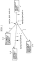
- Fig. 1 is a block diagram which shows one configuration example of a transmission system according to a point-to-multi-point optical time compression multiplexing transmission system to which the present invention can be applied.
- transmitted downward optical signals from equipment at a central office 1 is branched at optical star coupler 3 through the transmission line 4 which consists of optical fiber, optical connectors, etc. and is transmitted to more than one piece of equipment at subscriber premises 2-1, 2-2, ..., 2-n in broadcasting form through the transmission lines 4, 4, 4, ... which consists of optical connectors, etc.
- the above transmitted downward optical signals from equipment at a central office 1 are time division multiplexing optical signals being multiplexed with each sending optical signal to more than one subscriber in a time domain. Then, each piece of equipment at subscriber premises 2-1, 2-2, ..., 2-n chooses an optical signal for one's own equipment from these downward optical signals, i.e., the time division multiplexing optical signals toward more than one subscriber and receives it, respectively.
- each piece of equipment at subscriber premises 2-1, 2-2,..., 2-n transmits an upward optical signal in a time domain which is assigned to each piece of equipment at subscriber premises.
- These upward optical signals from more than one piece of equipment at subscriber premises 2-1, 2-2,..., 2-n join at the optical star coupler and are received by the equipment at a central office 1.
- A is the input/output terminal of the equipment at a central office and B1, B2,..., Bn are input/output terminals at each piece of equipment at subscriber premises 2-1, 2-2,..., 2-n.
- FIG. 2 one preferred embodiment of the internal configuration of the equipment at a central office 1 and each piece of equipment at subscriber premises 2-1, 2-2,..., 2-n which are shown in Fig. 1 will be explained. Because it is possible to make the internal configuration of each piece of equipment at subscriber premises 2-1, 2-2, ..., 2-n identically, an internal configuration of equipment at subscriber premises 2-n is shown in this figure as a representative example. Furthermore, identical reference signs are used for each component whose basic configuration is identical at both the equipment at a central office 1 and the equipment at subscriber premises 2-n.
- the equipment at a central office 1 shown in Fig. 2 is comprised of the following circuits and devices:
- the equipment at subscriber premises 2-n is comprised of the switch 101, the automatic gain control amplifier 102, the timing extraction and frame synchronization circuit 103, the decision circuit 104, the receiving buffer circuit 106, the transmission buffer circuit 105, the reset circuit 200 for the automatic gain control amplifier and the reset circuit 300 for the timing extraction and frame synchronization circuit, approximately in the same way as the equipment at a central office 1.
- the main differences between the equipment at subscriber premises 2-n and the equipment at a central office 1 are that equipment at subscriber premises 2-n does not contain clock circuit 108, that the switch 101 of the equipment at subscriber premises 2-n is switched according to the output of the timing extraction and frame synchronization circuit 103, and that the timing extraction and frame synchronization circuit 103 in the equipment at subscriber premises 2-n is equipped with a function which is necessary for extracting a signal for the subscriber's equipment from the signals for all equipment at the subscriber premises additionally. Then, the equipment at a central office 1 and the equipment at subscriber premises 2-n carry out optical time compression multiplexing transmission while they are connected to each other through the optical transmission lines 4, 4, 4,...
- the most characteristic portions of the present invention in the above configuration are the reset circuit 200 for the automatic gain control amplifier and the reset circuit 300 for the timing extraction and frame synchronization circuit which are provided for the equipment at a central office 1 and the equipment at subscriber premises 2-n, respectively.
- This reset circuit 200 for the automatic gain control amplifier is a circuit which is provided to prevent the automatic gain control amplifier from converging with the optical reflection.
- the reset circuit 300 for the timing extraction and frame synchronization circuit is a circuit which is provided to prevent mis-synchronization with the optical reflection.
- these circuits can operate independently. Therefore, these circuits may be equipped in both the equipment at a central office 1 and the equipment at subscriber premises 2-n, respectively, as shown in Fig. 2, or they may be equipped in one or the other equipment.
- Fig. 3 is a timing diagram which shows an example of the sending and receiving operation of a point-to-multi-point optical time compression multiplexing transmission system which has been explained referring to Fig. 1 and Fig. 2.
- Fig. 3 is a diagram on the assumption that there is a reflection point R1 between the equipment at a central office 1 and optical star coupler 3, which is shown in Fig. 1.
- This figure also shows the temporal change of the optical signals at the input/output terminal A of the equipment at a central office I and the input/output terminals B1,..., Bn of each piece of equipment at subscriber premises 2-1,...,2-n.
- signals are exchanged among the equipment at a central office 1 and each piece of equipment at subscriber premises 2-1, 2-2, ..., 2-n.
- Optical signals sent to each piece of equipment at subscriber premises 2-1, 2-2, ..., 2-n are transmitted as downward sending optical signals every burst repetition period from the equipment at a central office 1.
- sending optical signals to each piece of equipment at subscriber premises 2-1, 2-2, ..., 2-n are multiplexed by a time division multiplexing method within this downward sending optical signal frame "a" (input/output terminal A).
- This downward sending optical signals are received as downward receiving optical signals at each piece of equipment at the subscriber premises (input/output terminal B1, ..., Bn).
- each piece of equipment at the subscriber premises chooses a signal for each piece of equipment out of plural signals in the downward receiving optical signals.
- each piece of equipment at subscriber premises transmits upward sending optical signals b1, b2, ..., bn, respectively, in the time area which is respectively allocated for each piece of equipment (input/output terminal B1, ..., Bn). Then, these upward sending optical signals b1, b2, ..., bn are received in upward receiving optical signal frame b by the equipment at the central office 1 (input/output terminal A).
- Each transmission time of the upward sending optical signals b1, b2, ..., bn is assigned by control of the equipment at the central office 1 to each piece of equipment at subscriber premises, so that the upward optical signals of each piece of equipment at subscriber premises do not interfere with each other.
- a guard time T G is secured respectively in both changing to receiving from sending, and in changing to sending from receiving, at the equipment at the central office 1 and each subscriber equipment. That is, in this case, at the equipment at the central office 1, the switch 101 is switched from the side of sending to the side of receiving at time t A 2 after the T G period from time t A 1 when finishing transmitting the frame "a" of the downward sending optical signals, and in this condition, it is possible to receive signals. Then, the switch 101 is again switched at time t A 7 after the T G period from time t A 6 when finishing receiving the sending optical signal bn which places the end of the frame b of the upward receiving optical signals, and the condition returns to the sending one in which it is possible to send signals.
- each switch 101 is switched from the receiving side to the sending side after the T G period (at time t B12 ,..., t Bn2 ) from the rearmost part (at time t B11 ,..., t Bn1 ) of the frame "a" of the downward receiving optical signals, and the operation condition becomes a sending one, respectively.
- the changing of the opposite direction from the condition for sending to the other condition for receiving is carried out respectively after the T G period from the respective finishing time of sending of one of the subscriber's sending optical signals b1,..., bn at each piece of equipment at subscriber premises 2-1,..., 2-n.
- switching the switch 101 from the side of the sending to the side of the receiving at each piece of equipment at subscriber premises 2-1, ..., 2-n depends on the assignment position of each sending optical signal in the frame b of the upward sending optical signals. For example, when assigned to the forefront b1 (at the input/output terminal B1), switching is carried out at time t B 1 4 after the T G period from time t B 1 3 when finishing sending the sending optical signal b1. For example, when assigned to the rearmost part bn (at the input/output terminal Bn), switching is carried out at time t B n 4 after the T G period from time t B n 3 finishing sending the sending optical signal bn.
- each input/output terminal B1, ..., Bn of each piece of equipment at subscriber premises 2-1, ..., 2-n the optical reflection b1', b2', ..., bn' corresponding to the respective upward sending optical signals b1, b2, ..., bn from one of the subscriber's equipment or another subscriber's equipment is observed in the time which is equivalent to the round trip delay time between each of input/output terminals B1, B2,..., Bn and the reflection point R1.
- the reset circuit 200 for the automatic gain control amplifier which is shown in Fig. 2 watches the output signal of the decision circuit 104. Then, it outputs a reset signal to the automatic gain control amplifier 102 in case the duration of continuous "0" level of the output signals from the decision circuit 104 is equal to or more than a predetermined time.
- this reset circuit 200 for the automatic gain control amplifier may be realized simply by some logic circuits which count continuous "0" level signals.
- the above-mentioned predetermined time which is used as a standard for the decision of the reset circuit 200 for the automatic gain control amplifier whether to output a reset signal, may be set optionally. However, it is desirable to set the time as being equal to the guard time T G exactly or approximately.
- the automatic gain control amplifier 102 resets an amplification gain to maximum level when this reset signal is inputted.
- the operation condition of the equipment at the central office 1 is changed to the receiving condition from the sending condition at time t A 2 when the guard time T G passed after sending-out the sending frame "a".
- the optical reflection a' of the sending frame "a" which was caused by the reflection point R1 on the transmission line 4 exists at the input/output terminal A of the equipment at the central office 1 at time t A 2 . Therefore, the gain of the AGC amplifier 102 which received this optical reflection a' is automatically adjusted based on the level of the optical reflection a' and the gain is kept low. After that, the optical reflection a' disappears at time t A 3 and the output signal of the decision circuit 104 becomes "0".
- the reset circuit 200 for the automatic gain control amplifier is watching the output signal of the decision circuit 104 at this time, when the duration of the continuous "0" level condition becomes approximately equivalent to the guard time T G (at time t A 4 ), it outputs the first reset signal.
- the automatic gain control amplifier 102 is forced to be reset by this reset signal and the gain is set to the maximum level. Because the automatic gain control amplifier 102 amplifies the input signals at the maximum gain, even if the signal in the beginning of the following receiving frame b which is sent from each piece of equipment at the subscriber premises 2-1, 2-2, ..., 2-n and it is attenuated to a low level, the signal can be normally received without error in detection.
- the reset signal which is generated by the reset circuit 200 for the automatic gain control amplifier is repeatedly generated every time the duration of continuous "0" level approximately passes another guard time T G .
- a reset signal is generated again at time t A 5 when the guard time T G passed from time t A 4 when the first reset signal was generated.
- the "0" continuation signal which is longer than the guard time T G is contained in the frame b of the receiving signal, i.e. the upward receiving optical signal, the automatic gain control amplifier 102 is reset by mistake with a regular signals.
- the reset circuit 200 for the automatic gain control amplifier should be set so as not to operate during the receiving frame area.
- the reset circuit 200 for the automatic gain control amplifier is set so that it is always possible to operate in the condition of the proving in frame synchronization wherein the synchronization of the receiving frame b is not established, That is, it may be set to start operating at the rearmost part of the sending frame after synchronization is established, and to stop the operation at the beginning of the receiving frame.
- the reset circuit 200 for the automatic gain control amplifier in each piece of equipment at subscriber premises 2-1, 2-2,..., 2-n operates basically like the case of the above-mentioned equipment at the central office 1.
- the switch 101 is switched at time t B 1 4 after the guard time T G period from time t B 1 3 when it has completed sending the sending optical signal b1 in the upward sending optical signal frame b.
- the automatic gain control amplifier 102 becomes set at operation condition at time t B 1 4 where it is possible to receive signals, after that, the gain of the automatic gain control amplifier 102 is controlled according to the sending optical signals or optical reflection b1', b2',..., bn' caused by one of the subscriber's equipment, or coming from another equipment at the subscriber premises which are transmitted on the transmission line 4. Then, the reset circuit 200 for the automatic gain control amplifier in the equipment at subscriber premises 2-1 outputs a reset signal at time t B 1 6 after the guard time T G from time t B 1 5 when the optical reflection bn' is not observed at the input/output terminal B1.
- the gain of the automatic gain control amplifier 102 is reset in the maximum, and the beginning of the downward receiving optical signal in the following burst repetition period is received with an appropriate gain.
- the switch 101 is switched at time t B n 4 after the guard time T G from time t B n 3 when it has finished sending the sending optical signal bn in the upward sending optical signal frame b.
- the gain of the automatic gain control amplifier 102 is controlled according to the sending optical signals and the optical reflection from a subscriber's equipment and other equipment at the subscriber premises on the transmission line 4.
- the reset circuit 200 for the automatic gain control amplifier of the equipment at subscriber premises 2-n outputs a reset signal at time t B n 6 after the guard time T G from time t B n 5 when the optical reflection bn' corresponding to the sending optical signal bn from the same equipment had not been observed at the input/output terminal Bn. Therefore, at this time, the gain of the automatic gain control amplifier 102 is reset in the maximum, and the beginning of the downward receiving optical signal of the following burst repetition period is received at an appropriate gain.
- the attenuation of the optical reflection which occurs between the input/output terminal A and the reflection point R2 becomes large as well as the duration becomes long because an optical star coupler is contained in the route of the optical reflection. Because the signal level of the optical reflection becomes sufficiently lower than the upward receiving optical signal and the automatic gain control amplifier 102 can follow the upward receiving optical signal of the following without delay, even if having converged on the optical reflection, the influence of the optical to the automatic gain control amplifier 102 can be ignored.
- the power of the optical reflection corresponding to the sending optical signal from one of subscriber's equipment, which occurs at the reflection point R2 becomes large at the input/output terminal B2 of the equipment at subscriber premises 2-2.
- the reset circuit 200 of equipment at subscriber premises 2-2 for the automatic gain control amplifier outputs a reset signal to the automatic gain control amplifier 102. Therefore, the mis-convergence of the automatic gain control amplifier 102 to the optical reflection never exerts a deleterious influence on the receiving of the downward receiving optical signals in the following burst repetition period.
- the automatic gain control amplifier 102 shown in this figure consists of an operational amplifier, a fixed resistance as a negative feedback resistance, a FET as an input resistance, a condenser, a diode, a direct current bias power supply, and a transistor which is connected to the condenser and so on.
- the charging and discharging of the electric charge to this condenser are controlled according to the signal at the output terminal of the operational amplifier.
- the transistor which is connected to the condenser is provided for discharging the electric charge of this condenser and it operates according to the reset signal from the reset circuit 200 for the automatic gain control amplifier.
- the resistance value of the FET is made to be large by discharging the electric charge of the condenser and the gain of the operational amplifier is set at a given maximum value immediately after a reset signal is sent from the reset circuit 200 for the automatic gain control amplifier to the automatic gain control amplifier 102.
- a reset signal is sent from the reset circuit 200 for the automatic gain control amplifier to the automatic gain control amplifier 102.
- each switch 101 in each piece of equipment is switched to the side of the sending in the equipment at the central office 1 and each piece of equipment at subscriber premises 2-1, 2-2,..., 2-n which are shown in Fig. 1 and Fig. 2. Therefore, an optical signal from a subscriber's equipment is never directly inputted to each automatic gain control amplifier 102.
- each switch 101 is switched to the side of the receiving respectively, and each piece of equipment respectively changes to be in a condition in which it is possible to receive signals.
- an automatic gain control amplifier 102 controls its gain according to the amplitude level of the optical reflection and it keeps output amplitude at an appropriate level. Then, the timing extraction and frame synchronization circuit 107 or 103 operate to establish synchronization according to the output of this automatic gain control amplifier 102 in the equipment at the central office 1 or in each piece of equipment at subscriber premises 2-1, 2-2, ..., 2-n. If a bit pattern which is identical to the frame pattern of the regular receiving optical signal exists in the optical reflection at this time, the frame pattern of the regular receiving optical signal which follows becomes unable to be detected because the timing extraction and frame synchronization circuit 107 or 103 has established the frame synchronization of the optical reflection.
- the reset circuit 300 for the timing extraction and frame synchronization circuit watches over the output of the decision circuit 104 and determines whether or not the receiving signal is a regular signal, and when the receiving signal is determined to not be a regular signal, it operates to reset the timing extraction and frame synchronization circuit 103. Therefore, the probability that the frame pattern of the following regular receiving optical signals becomes unable to be detected can be made small.
- the condition transition of the point-to-multi-point of optical time compression multiplexing transmission system which is shown in Fig. 2 during the process of the frame synchronization establishment will be explained.
- the transition transfers to the proving in the frame synchronization condition when detecting a frame pattern in the frame hunting condition (in a condition of mis-synchronization) as shown in this figure.
- the reset circuit 300 for the timing extraction and frame synchronization circuit resets the timing extraction and frame synchronization circuit 103 and returns to the frame hunting condition.
- the transition transfers to the synchronous condition when detecting frame patterns of a fixed constant number continuously at the frame pattern position of the following frame in the proving in frame synchronization condition.
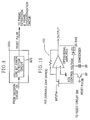
- Fig. 6 is a schematic diagram which shows an example of a sending frame which is used in the point-to-multi-point optical time compression multiplexing transmission system which is shown in Fig. 2.
- the sending frame which is shown in this figure is comprised of a frame pattern bit Fr used for frame synchronization, an overhead bit Oh to transmit maintenance information, sending data (Data) which consists of communication signals, and CRC (Cyclic Redundancy Check) inspection bit CRC for detecting faults.
- the overhead bit Oh or the cyclic redundancy check inspection bit CRC which are shown in Fig. 6 are used as supplementary information for the frame synchronization in the process of the frame synchronization establishment.
- Fig. 7 is a block diagram which shows a configuration example of the reset circuit 300 which is shown in the Fig. 2 when it uses the overhead bit Oh which is shown in Fig. 6 as the supplementary information for the frame synchronization.
- the receiving signal from the decision circuit 104 which is shown in Fig. 2 is inputted to an overhead bit separation circuit 301 which is shown in Fig. 7, and then the overhead bit Oh is separated from the receiving signal.
- bit pattern coincidence detection circuit 302 checks for a match between the overhead bit Oh and a predetermined bit pattern, and in case a discrepancy is detected, it sends out a reset pulse to the timing extraction and frame synchronization circuit 103.
- timing extraction and frame synchronization circuit 103 or 107 detects a bit pattern which is identical with the regular frame pattern bit Fr in the optical reflection, the synchronous establishment never continues in this condition as it synchronizes with that bit pattern according to the above-mentioned embodiment in the above-mentioned way. Therefore, only the original receiving signal which follows the frame pattern bit Fr and the overhead bit Oh according to a regular sending frame becomes able to be normally received in the higher probability.
- Fig. 8 is a block diagram which shows a configuration example of the reset circuit 300 when using the CRC inspection bit CRC which is shown in Fig. 6 as a supplementary information for the frame synchronization.
- a receiving signal from the decision circuit 104 is inputted to a CRC error detection circuit 303.
- the CRC error detection circuit 303 sends out a reset pulse to the timing extraction and frame synchronization circuit 103 when a CRC error is detected. Even if a bit pattern which is identical with the frame pattern Fr exists in the optical reflection, because the probability that the corresponding CRC inspection bit exists is very low, it is determined that there is an error as a result of the error detection in most of the cases and the timing extraction and frame synchronization circuit 103 is reset by a reset pulse. Therefore, it is possible to more certainly avoid continuing mis-synchronization conditions. It is also possible that the reset circuit 300 is comprised using both of the overhead bit Oh and the CRC inspection bit CRC.
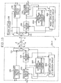
- Fig. 9 shows one such example.
- a reset pulse is sent out to the timing extraction and frame synchronization circuit 103 according to logical add of the reset pulse sending-out condition when using the overhead bit Oh and the other one when using CRC inspection bit CRC, which are respectively described above. Therefore, in this case, the mis-synchronization probability can be further reduced than by using either the overhead bit Oh or the CRC inspection bit CRC separately.
- a certain sending data can be used as supplementary information for the frame synchronization.
- some fixed pattern e.g., all "0", all "1", etc.
- the detection of such bit patterns and the reset of the timing extraction and frame synchronization circuit 103 in case of detecting a discrepancy are carried out, whereby the probability of receiving the following original receiving signal becomes high to avoid mis-synchronization as in the case of the use of the overhead bit Oh or the CRC inspection bit CRC.
- Fig. 10 is a block schematic diagram of an optical time compression multiplexing transmission system as another embodiment of the present invention, using identical reference signs for the parts which correspond to those in Fig. 2, and explanation of these parts which have been described above will be omitted.
- the system which is shown in Fig. 10 comprises equipment at a central office 1a and equipment at subscriber premises 2a-n.
- An ATC (automatic threshold level control) decision circuit 109 is provided in each piece of equipment in Fig. 10 instead of the automatic gain control amplifier 102 and the decision circuit 104 in Fig. 2.
- the ATC decision circuit 109 is a circuit which determines the level of receiving signals while automatically adjusting the threshold, which is a decision level, to an appropriate level.
- This ATC decision circuit 109 is comprised of a circuit which changes the receiving optical signal which is sent from transmission line 4 into an electrical signal, a circuit which changes the signal which was changed into the electrical signal into binary data by comparing it from a fixed threshold value, i.e. a decision level, a circuit which adjusts this threshold value according to the amplitude of the electrical signal, and so on.
- a fixed threshold value i.e. a decision level
- the ATC decision circuit 109 is reset by the reset signal which is outputted from the reset circuit 400 for the ATC decision circuit, it resets the decision level to the minimum one.
Description
- The present invention relates to an optical time compression multiplexing transmission system.
- Studies of various optical subscriber systems to realize FTTH (Fiber To the Home) are being conducted in every country at present.
- As one of the systems to realize this FTTH, studies and developments of a passive double star (PDS) optical subscriber system are being conducted. In the PDS optical subscriber system, an optical star coupler, which is a passive optical device, is arranged at branch points on optical transmission lines. Then, time division bidirectional communication is carried out between equipment at a central office and more than one piece of equipment at subscriber premises. In this system, time division bidirectional communication is generally realized on a single optical fiber by multiplexing downward optical signals from equipment at a central office to more than one piece of equipment at subscriber premises and upward optical signals from these pieces of equipment at subscriber premises to the equipment at a central office in time domain with TCM (Time Compression Multiplexing). Moreover, as a multiplexing method of optical signals to more than one piece of equipment at subscriber premises, TDMA (Time Division Multiple Access) method which multiplexes these signals in the time domain is used.
- In an optical transmission line, reflection occurs at parts, such as optical connectors and so on, which comprise a transmission line. Optical reflection which occurrs by reflection returns to a transmission terminal again at the time which is equivalent to a round trip delay time from the transmission terminal, where the optical signal was transmitted, to the reflection point, and is received at the transmission terminal.
- In a bidirectional transmission on a single optical fiber by the TCM-TDMA method, the following problems occur due to this optical reflection, and the receiving characteristic is degraded by these problems.
- Generally, an optical receiving circuit of an optical transmission system is equipped with an automatic gain control amplifier to keep output amplitude at an appropriate level by controlling a degree of amplification according to the input level of received optical signals. Regardless of whether the received light is an optical reflection, the automatic gain control amplifier controls a degree of amplification according to the input level of the received light/optical signal. Therefore, if the power of an optical reflection is high, and when using the gain which was controlled according to this optical reflection, the signal which should be received originally and follows the optical reflection cannot be sufficiently amplified. For example, when the electrical amplitude level of an optical reflection after changing the optical reflection into an electrical signal is greater than twice of the electrical amplitude level of the receiving optical signal which follows the optical reflection, a problem of mistaking a signal which was originally "1" as the signal "0" occurs.
- When a bit pattern which is identical with a frame pattern of a regular receiving optical signal exists in an optical reflection, frame synchronization must be established by the optical reflection by mistake and the regular received optical signal which follows the optical reflection is thereby not able to be received probably.
- It is thought that one of the solutions to the above-mentioned mis-convergence of the automatic gain control amplifier is to set a guard time between sending and receiving optical signals sufficiently longer than the time constant of gain control of the automatic gain control amplifier. In this way, it is possible to make the gain of the automatic gain control amplifier converge during the guard time after the optical reflection passes. However, the time constant of the gain control is set sufficiently long compared with the time width of 1 bit signal to prevent the gain from being changed by noise influence and/or "0", "1" pattern effect of receiving signals. Therefore, it becomes necessary to set the length of the guard time to be very long so as to set the length of the guard time to be sufficiently longer than the time constant of the gain control. As a result, the time area for sending and receiving optical signals narrows and transmission efficiency declines.
- In addition, the above-mentioned guard time is a constant time which is provided to secure idle-time which is necessary to change the operation condition between transmission and reception. This guard time is set respectively at both the equipment at the central office and the equipment at subscriber premises. During this guard time, no optical signal is transmitted from each piece of equipment. That is, the output level from each piece of equipment during the guard time is continuously "0".
- On the other hand, another measure to prevent the mis-synchronization to the optical reflection is to make the frame pattern length sufficiently long. This measure can lower the probability of existence of a bit pattern in the optical reflection, which is identical with a frame pattern of a regular receiving optical signal. However, there is a problem in that the transmission efficiency declines in this case, too.
- A fiber optic system based on a passive double star (PDS) architecture is known from the paper "Fiber-Optic Subscriber System Based on Passive Optical Network Architecture". Kitazawa et al. Hitachi review, vol. 43, no. 2, 1 April 1994, pages 53-58.
- A time compression multiplex digital transmission system dealing with the problem of establishing frame synchronization is disclosed by US-A-4 637 016 patent document.
- The following references show examples of the conventional art in automatic gain control amplifiers which are used by the subscriber systems. However, there are some problems in the conventional techniques described in these references. No consideration is given to the optical reflection whose occurrence cannot be controlled, or even if consideration is supposed to be given, the configuration is complicated or transmission efficiency has been decreased.
Conventional Art Reference 1) Fumio Mano, et al., "A study of fast-response AGC circuit for passive double star (PDS) optical subscriber systems", the electronic information communication society, Meeting, 1991, B-602.
Conventional Art Reference 2) Japanese Patent Application, First Publication, Sho 57-136831, "Receiving AGC control method"
Conventional Art Reference 3) Japanese Patent Application, First Publication, Hei 1-137752, "Receiving circuit" - The present invention is made in view of the above-mentioned problems. It is an object of the present invention to provide an optical time compression multiplexing transmission system which can reduce the influence of optical reflection by simple configuration without decreasing transmission efficiency.
- The present invention is a time division multiplexing point-to-multi-point optical time compression multiplexing transmission system which provides time division 1:n multiplexing bidirectional transmission between equipment at a central office and n (n is natural number) sets of equipment at subscriber premises, connected to each other, through single optical fibers.
- Each equipment is comprised of the following:
- a receiving means for receiving an optical signal, a decision means for deciding whether or not the received signal which was outputted from the receiving means is a regular signal, and an initialization means for initializing the operation condition of said receiving means when a received signal is determined to not be a regular signal by the decision means
-
- In operation according to the above configuration, after deciding whether or not the receiving signal is a regular signal at the decision means, the initialization means initializes the operation condition of the receiving means in case of not being a regular signal based on the decision result. Therefore, even if reflection exists in an optical transmission line, the operation condition of the receiving means, which has become irregular due to optical reflection can be initialized to a normal operation in a minimum time.
- As a result, optical time compression multiplexing transmission with good efficiency can be realized.
- Further objects and advantages of the present invention will be apparent from the following description and the accompanying drawings wherein preferred embodiments of the present invention are clearly shown.
- In the drawings:
- Fig. 1 is a block diagram which shows a configuration example of a point-to-multi-point optical time compression multiplexing transmission system including a star coupler which is possible to be applied to the present invention.
- Fig. 2 is a block diagram which shows a configuration of a point-to-multi-point time division multiplexing optical time compression multiplexing transmission system which is an embodiment of the present invention.
- Fig. 3 is a sending and receiving diagram of the point-to-multi-point time division multiplexing optical time compression multiplexing transmission system which is shown in Fig. 2.
- Fig. 4 is another sending and receiving diagram of a different condition from Fig. 3 in the point-to-multi-point the time division multiplexing optical time compression multiplexing transmission system which is shown in Fig. 2.
- Fig. 5 is a condition transition diagram which shows condition transition in the process of a frame synchronization establishment with the embodiment which is shown in Fig. 2.
- Fig. 6 is a schematic diagram which shows the one configuration example of a transmission frame which can be used for the point-to-multi-point time division multiplexing optical time compression multiplexing transmission system which is shown in Fig. 2.
- Fig. 7 is a block diagram which shows an example of an internal configuration of the
reset circuit 300 for the timing extraction and frame synchronization circuit which is shown in Fig. 2. - Fig. 8 is a block diagram which shows another configuration example of the
reset circuit 300 for the timing extraction and frame synchronization circuit which is shown in Fig. 2. - Fig. 9 is a block diagram which shows the other configuration example of the
reset circuit 300 for the timing extraction and frame synchronization circuit which is shown in Fig. 2. - Fig. 10 is a block diagram which shows a configuration of the optical time compression multiplexing transmission system according to another embodiment of the present invention.
- Fig. 11 is a schematic diagram which shows one configuration example of the
automatic
gain control amplifier 102 which is shown in Fig. 2. -
- Fig. 1 is a block diagram which shows one configuration example of a transmission system according to a point-to-multi-point optical time compression multiplexing transmission system to which the present invention can be applied. In the point-to-multi-point optical transmission system which is shown in this figure, transmitted downward optical signals from equipment at a
central office 1 is branched atoptical star coupler 3 through thetransmission line 4 which consists of optical fiber, optical connectors, etc. and is transmitted to more than one piece of equipment at subscriber premises 2-1, 2-2, ..., 2-n in broadcasting form through thetransmission lines central office 1 are time division multiplexing optical signals being multiplexed with each sending optical signal to more than one subscriber in a time domain. Then, each piece of equipment at subscriber premises 2-1, 2-2, ..., 2-n chooses an optical signal for one's own equipment from these downward optical signals, i.e., the time division multiplexing optical signals toward more than one subscriber and receives it, respectively. - At the other end, in the upward transmission to the equipment at the central office, each piece of equipment at subscriber premises 2-1, 2-2,..., 2-n (n is a natural number) transmits an upward optical signal in a time domain which is assigned to each piece of equipment at subscriber premises. These upward optical signals from more than one piece of equipment at subscriber premises 2-1, 2-2,..., 2-n join at the optical star coupler and are received by the equipment at a
central office 1. In Fig. 1, A is the input/output terminal of the equipment at a central office and B1, B2,..., Bn are input/output terminals at each piece of equipment at subscriber premises 2-1, 2-2,..., 2-n. - Next, referring to Fig. 2, one preferred embodiment of the internal configuration of the equipment at a
central office 1 and each piece of equipment at subscriber premises 2-1, 2-2,..., 2-n which are shown in Fig. 1 will be explained. Because it is possible to make the internal configuration of each piece of equipment at subscriber premises 2-1, 2-2, ..., 2-n identically, an internal configuration of equipment at subscriber premises 2-n is shown in this figure as a representative example. Furthermore, identical reference signs are used for each component whose basic configuration is identical at both the equipment at acentral office 1 and the equipment at subscriber premises 2-n. - The equipment at a
central office 1 shown in Fig. 2 is comprised of the following circuits and devices: - a
clock circuit 108 which generates a clock signal; - a
switch 101 which switches transmission and receiving according to the clock from theclock circuit 108; - an AGC (automatic gain control)
amplification circuit 102 which changes a receiving optical signal outputted from theswitch 101 into an electric signal, and amplifies it while adjusting a degree of the amplification to keep its output amplitude level at an appropriate level, and outputs the amplified receiving signal (in addition, the automaticgain control amplifier 102 may be modified in order that it amplifies a receiving optical signal before changing it into an electrical signal while adjusting the gain, and after that, changes the amplified optical signal into an electric signal.); - a timing extraction and frame synchronization circuit 107 which accomplishes timing
extraction and frame synchronization based on the output signal of the automatic
gain control amplifier 102; - a
decision circuit 104 which distinguishes "0"/"1" of the receiving signal based on the output of automaticgain control amplifier 102; - a receiving
buffer circuit 106 which once stores burst data which is outputted from thedecision circuit 104, and outputs the data at a original data speed; - a
transmission buffer circuit 105 to output optical signals as burst data according to the clocks from theclock circuit 108 after storing inputted transmission data from an input terminal and changing it into optical signals; - the above-mentioned
switch 101 which switches sending/receiving mode based on the clocks from theclock circuit 108; - a
reset circuit 200 for the automatic gain control amplifier which resets the gain of the automaticgain control amplifier 102 based on the output from thedecision circuit 104; and - a
reset circuit 300 for the timing extraction and frame synchronization circuit which resets the synchronous condition of the timing extraction and frame synchronization circuit 107 based on the output from thedecision circuit 104. -
- Incidentally, plural signal lines are laid down among each of the blocks in the above-mentioned configuration but are not illustrated, and outputs of the
clock circuit 108, the timing extraction and frame synchronization circuit 107 and so on are transferred among each of the blocks through them. - On the other hand, the equipment at subscriber premises 2-n is comprised of the
switch 101, the automaticgain control amplifier 102, the timing extraction andframe synchronization circuit 103, thedecision circuit 104, the receivingbuffer circuit 106, thetransmission buffer circuit 105, thereset circuit 200 for the automatic gain control amplifier and thereset circuit 300 for the timing extraction and frame synchronization circuit, approximately in the same way as the equipment at acentral office 1. - The main differences between the equipment at subscriber premises 2-n and the equipment at a
central office 1 are that equipment at subscriber premises 2-n does not containclock circuit 108, that theswitch 101 of the equipment at subscriber premises 2-n is switched according to the output of the timing extraction andframe synchronization circuit 103, and that the timing extraction andframe synchronization circuit 103 in the equipment at subscriber premises 2-n is equipped with a function which is necessary for extracting a signal for the subscriber's equipment from the signals for all equipment at the subscriber premises additionally. Then, the equipment at acentral office 1 and the equipment at subscriber premises 2-n carry out optical time compression multiplexing transmission while they are connected to each other through theoptical transmission lines optical star coupler 3, and switch therespective switch 101 alternately according to both receiving and transmission modes. In particular, the most characteristic portions of the present invention in the above configuration are thereset circuit 200 for the automatic gain control amplifier and thereset circuit 300 for the timing extraction and frame synchronization circuit which are provided for the equipment at acentral office 1 and the equipment at subscriber premises 2-n, respectively. Thisreset circuit 200 for the automatic gain control amplifier is a circuit which is provided to prevent the automatic gain control amplifier from converging with the optical reflection. Thereset circuit 300 for the timing extraction and frame synchronization circuit is a circuit which is provided to prevent mis-synchronization with the optical reflection. Moreover, these circuits can operate independently. Therefore, these circuits may be equipped in both the equipment at acentral office 1 and the equipment at subscriber premises 2-n, respectively, as shown in Fig. 2, or they may be equipped in one or the other equipment. - The basic operation of the optical time compression multiplexing transmission system which is shown in Fig. 2 will be explained here before the details of
reset circuit 200 for the automatic gain control amplifier and thereset circuit 300 for the timing extraction and frame synchronization circuit are explained. - Fig. 3 is a timing diagram which shows an example of the sending and receiving operation of a point-to-multi-point optical time compression multiplexing transmission system which has been explained referring to Fig. 1 and Fig. 2. In addition, Fig. 3 is a diagram on the assumption that there is a reflection point R1 between the equipment at a
central office 1 andoptical star coupler 3, which is shown in Fig. 1. This figure also shows the temporal change of the optical signals at the input/output terminal A of the equipment at a central office I and the input/output terminals B1,..., Bn of each piece of equipment at subscriber premises 2-1,...,2-n. By changing sending and receiving alternately at each burst repetition period unit in the system which is shown in Fig. 1, signals are exchanged among the equipment at acentral office 1 and each piece of equipment at subscriber premises 2-1, 2-2, ..., 2-n. Optical signals sent to each piece of equipment at subscriber premises 2-1, 2-2, ..., 2-n are transmitted as downward sending optical signals every burst repetition period from the equipment at acentral office 1. In this case, sending optical signals to each piece of equipment at subscriber premises 2-1, 2-2, ..., 2-n are multiplexed by a time division multiplexing method within this downward sending optical signal frame "a" (input/output terminal A). This downward sending optical signals are received as downward receiving optical signals at each piece of equipment at the subscriber premises (input/output terminal B1, ..., Bn). Then, each piece of equipment at the subscriber premises chooses a signal for each piece of equipment out of plural signals in the downward receiving optical signals. - On the other hand, in the upward direction, each piece of equipment at subscriber premises transmits upward sending optical signals b1, b2, ..., bn, respectively, in the time area which is respectively allocated for each piece of equipment (input/output terminal B1, ..., Bn). Then, these upward sending optical signals b1, b2, ..., bn are received in upward receiving optical signal frame b by the equipment at the central office 1 (input/output terminal A). Each transmission time of the upward sending optical signals b1, b2, ..., bn is assigned by control of the equipment at the
central office 1 to each piece of equipment at subscriber premises, so that the upward optical signals of each piece of equipment at subscriber premises do not interfere with each other. Also, a guard time TG is secured respectively in both changing to receiving from sending, and in changing to sending from receiving, at the equipment at thecentral office 1 and each subscriber equipment. That is, in this case, at the equipment at thecentral office 1, theswitch 101 is switched from the side of sending to the side of receiving at time tA 2 after the TG period from time tA 1 when finishing transmitting the frame "a" of the downward sending optical signals, and in this condition, it is possible to receive signals. Then, theswitch 101 is again switched at time tA 7 after the TG period from time tA 6 when finishing receiving the sending optical signal bn which places the end of the frame b of the upward receiving optical signals, and the condition returns to the sending one in which it is possible to send signals. - On the other hand, in each piece of equipment at subscriber premises 2-1,..., 2-n, each
switch 101 is switched from the receiving side to the sending side after the TG period (at time tB12,..., tBn2) from the rearmost part (at time tB11,..., tBn1) of the frame "a" of the downward receiving optical signals, and the operation condition becomes a sending one, respectively. Then, the changing of the opposite direction from the condition for sending to the other condition for receiving is carried out respectively after the TG period from the respective finishing time of sending of one of the subscriber's sending optical signals b1,..., bn at each piece of equipment at subscriber premises 2-1,..., 2-n. Therefore, switching theswitch 101 from the side of the sending to the side of the receiving at each piece of equipment at subscriber premises 2-1, ..., 2-n depends on the assignment position of each sending optical signal in the frame b of the upward sending optical signals. For example, when assigned to the forefront b1 (at the input/output terminal B1), switching is carried out at time tB 1 4 after the TG period from time tB 1 3 when finishing sending the sending optical signal b1. For example, when assigned to the rearmost part bn (at the input/output terminal Bn), switching is carried out at time tB n 4 after the TG period from time tB n 3 finishing sending the sending optical signal bn. - Next, the optical reflection which occurs at reflection point R1 will be explained. Download sending optical signal frame "a" which has been sent from the equipment at the
central office 1 is reflected at the reflection point R1 and returns to the equipment at thecentral office 1 as an optical reflection a'. During the period which is equivalent to the round trip delay time between the input/output terminal A and the reflection point R1 from time tA 1 when the rearmost of the downward optical sending signal frame "a" was sent from the input/output terminal A, the optical reflection a' is observed continuously at the central office 1 (during time tA 1- tA 3). - On the other hand, at each input/output terminal B1, ..., Bn of each piece of equipment at subscriber premises 2-1, ..., 2-n, the optical reflection b1', b2', ..., bn' corresponding to the respective upward sending optical signals b1, b2, ..., bn from one of the subscriber's equipment or another subscriber's equipment is observed in the time which is equivalent to the round trip delay time between each of input/output terminals B1, B2,..., Bn and the reflection point R1.
- Next, the details of the
reset circuit 200 for the automatic gain control amplifier will be explained. - The
reset circuit 200 for the automatic gain control amplifier which is shown in Fig. 2 watches the output signal of thedecision circuit 104. Then, it outputs a reset signal to the automaticgain control amplifier 102 in case the duration of continuous "0" level of the output signals from thedecision circuit 104 is equal to or more than a predetermined time. For example, thisreset circuit 200 for the automatic gain control amplifier may be realized simply by some logic circuits which count continuous "0" level signals. The above-mentioned predetermined time, which is used as a standard for the decision of thereset circuit 200 for the automatic gain control amplifier whether to output a reset signal, may be set optionally. However, it is desirable to set the time as being equal to the guard time TG exactly or approximately. Moreover, the automaticgain control amplifier 102 resets an amplification gain to maximum level when this reset signal is inputted. - Next, referring to Fig. 3, it will be explained how the
reset circuit 200 for the automatic gain control amplifier operates. - As explained above referring to Fig. 3, the operation condition of the equipment at the
central office 1 is changed to the receiving condition from the sending condition at time tA 2 when the guard time TG passed after sending-out the sending frame "a". In the case shown in Fig. 3, the optical reflection a' of the sending frame "a" which was caused by the reflection point R1 on thetransmission line 4 exists at the input/output terminal A of the equipment at thecentral office 1 at time tA 2. Therefore, the gain of theAGC amplifier 102 which received this optical reflection a' is automatically adjusted based on the level of the optical reflection a' and the gain is kept low. After that, the optical reflection a' disappears at time tA 3 and the output signal of thedecision circuit 104 becomes "0". Because thereset circuit 200 for the automatic gain control amplifier is watching the output signal of thedecision circuit 104 at this time, when the duration of the continuous "0" level condition becomes approximately equivalent to the guard time TG (at time tA 4), it outputs the first reset signal. The automaticgain control amplifier 102 is forced to be reset by this reset signal and the gain is set to the maximum level. Because the automaticgain control amplifier 102 amplifies the input signals at the maximum gain, even if the signal in the beginning of the following receiving frame b which is sent from each piece of equipment at the subscriber premises 2-1, 2-2, ..., 2-n and it is attenuated to a low level, the signal can be normally received without error in detection. Furthermore, the reset signal which is generated by thereset circuit 200 for the automatic gain control amplifier is repeatedly generated every time the duration of continuous "0" level approximately passes another guard time TG. In the example which is shown in Fig. 3, a reset signal is generated again at time tA 5 when the guard time TG passed from time tA 4 when the first reset signal was generated. Incidentally, in the case of always setting thereset circuit 200 for the automatic gain control amplifier at the operation condition, if the "0" continuation signal which is longer than the guard time TG is contained in the frame b of the receiving signal, i.e. the upward receiving optical signal, the automaticgain control amplifier 102 is reset by mistake with a regular signals. To prevent this, after a frame synchronization is established, thereset circuit 200 for the automatic gain control amplifier should be set so as not to operate during the receiving frame area. Thereset circuit 200 for the automatic gain control amplifier is set so that it is always possible to operate in the condition of the proving in frame synchronization wherein the synchronization of the receiving frame b is not established, That is, it may be set to start operating at the rearmost part of the sending frame after synchronization is established, and to stop the operation at the beginning of the receiving frame. - On the other hand, the
reset circuit 200 for the automatic gain control amplifier in each piece of equipment at subscriber premises 2-1, 2-2,..., 2-n operates basically like the case of the above-mentioned equipment at thecentral office 1. For example, at the equipment at subscriber premises 2-1, theswitch 101 is switched at time tB 1 4 after the guard time TG period from time tB 1 3 when it has completed sending the sending optical signal b1 in the upward sending optical signal frame b. In this case, because the automaticgain control amplifier 102 becomes set at operation condition at time tB 1 4 where it is possible to receive signals, after that, the gain of the automaticgain control amplifier 102 is controlled according to the sending optical signals or optical reflection b1', b2',..., bn' caused by one of the subscriber's equipment, or coming from another equipment at the subscriber premises which are transmitted on thetransmission line 4. Then, thereset circuit 200 for the automatic gain control amplifier in the equipment at subscriber premises 2-1 outputs a reset signal at time tB 1 6 after the guard time TG from time tB 1 5 when the optical reflection bn' is not observed at the input/output terminal B1. Therefore, at this time, the gain of the automaticgain control amplifier 102 is reset in the maximum, and the beginning of the downward receiving optical signal in the following burst repetition period is received with an appropriate gain. In addition, for example, in the equipment at subscriber premises 2-n, theswitch 101 is switched at time tB n 4 after the guard time TG from time tB n 3 when it has finished sending the sending optical signal bn in the upward sending optical signal frame b. In this case, because the automaticgain control amplifier 102 is in the condition at which it can receive signals at time tB n 4, after that, the gain of the automaticgain control amplifier 102 is controlled according to the sending optical signals and the optical reflection from a subscriber's equipment and other equipment at the subscriber premises on thetransmission line 4. Then, thereset circuit 200 for the automatic gain control amplifier of the equipment at subscriber premises 2-n outputs a reset signal at time tB n 6 after the guard time TG from time tB n 5 when the optical reflection bn' corresponding to the sending optical signal bn from the same equipment had not been observed at the input/output terminal Bn. Therefore, at this time, the gain of the automaticgain control amplifier 102 is reset in the maximum, and the beginning of the downward receiving optical signal of the following burst repetition period is received at an appropriate gain. Although the timing when thereset circuit 200 for the automatic gain control amplifier outputs a reset signal differs depending upon the assigned position of the sending optical signal in the equipment at subscriber premises 2-1, there should be no difference in the problem of the mis-convergence of the gain of the automaticgain control amplifier 102 to the optical reflection being solved before the following burst repetition period begins. Incidentally, when an optical reflection of a frame is not received for a long period, because the period of the continuous "0" level also becomes long, plural reset signals are repeatedly outputted at the cycle of TG (at times tB 1 7, tB n 7) until the next receiving optical signal is received. - Next, referring to Fig. 4, it will be explained how the
reset circuit 200 for the automatic gain control amplifier operates when there is another reflection point R2 between theoptical star coupler 3 and the equipment at subscriber premises 2-2, which is shown in Fig. 1. - However, in this case, it should be possible to ignore a reflection at the reflection point R1 which is shown in Fig. 1. In this condition, in the equipment at the
central office 1, the round trip delay time from the input/output terminal A to the reflection point R2 becomes longer compared with the case shown in Fig. 3, and the duration of the optical reflection of the downward sending optical signals becomes long. Therefore, in some cases, the period of continuous "0" until the beginning of the upward receiving optical signals after the optical reflection disappears becomes short as shown in Fig. 4, and thereset circuit 200 for the automatic gain control amplifier might sometimes generate no reset signal. However, in this case, the attenuation of the optical reflection which occurs between the input/output terminal A and the reflection point R2 becomes large as well as the duration becomes long because an optical star coupler is contained in the route of the optical reflection. Because the signal level of the optical reflection becomes sufficiently lower than the upward receiving optical signal and the automaticgain control amplifier 102 can follow the upward receiving optical signal of the following without delay, even if having converged on the optical reflection, the influence of the optical to the automaticgain control amplifier 102 can be ignored. - On the other hand, the power of the optical reflection corresponding to the sending optical signal from one of subscriber's equipment, which occurs at the reflection point R2, becomes large at the input/output terminal B2 of the equipment at subscriber premises 2-2. However, at least once until the beginning of the following burst repetition period after receiving this optical reflection, the
reset circuit 200 of equipment at subscriber premises 2-2 for the automatic gain control amplifier outputs a reset signal to the automaticgain control amplifier 102. Therefore, the mis-convergence of the automaticgain control amplifier 102 to the optical reflection never exerts a deleterious influence on the receiving of the downward receiving optical signals in the following burst repetition period. - Incidentally, various well-known circuits can be used as the above-mentioned automatic
gain control amplifier 102 which is possible to be reset by thereset circuit 200 for the automatic gain control amplifier; here, with reference to Fig. 11, one configuration example of the automatic gain control amplifier whose gain is possible to be reset will be explained. The automaticgain control amplifier 102 shown in this figure consists of an operational amplifier, a fixed resistance as a negative feedback resistance, a FET as an input resistance, a condenser, a diode, a direct current bias power supply, and a transistor which is connected to the condenser and so on. As the gate of this FET being connected to the condenser, the charging and discharging of the electric charge to this condenser are controlled according to the signal at the output terminal of the operational amplifier. The transistor which is connected to the condenser is provided for discharging the electric charge of this condenser and it operates according to the reset signal from thereset circuit 200 for the automatic gain control amplifier. By controlling the electric charge to charge the condenser with a feedback control method according to the output of the operational amplifier by such configuration, the resistance value between drain-source of the FET is changed to adjust the gain of the operational amplifier, and the amplitude of the output signal can be kept at a fixed value. The resistance value of the FET is made to be large by discharging the electric charge of the condenser and the gain of the operational amplifier is set at a given maximum value immediately after a reset signal is sent from thereset circuit 200 for the automatic gain control amplifier to the automaticgain control amplifier 102. When using a configuration in this example, it is possible to fabricate the automatic gain control amplifier which is possible to be reset at the maximum gain only by the addition of some simple circuit parts. - Next, the details of the
reset circuit 300 for the timing extraction and frame synchronization circuit will be explained. As mentioned above, in the time area of the sending frame, eachswitch 101 in each piece of equipment is switched to the side of the sending in the equipment at thecentral office 1 and each piece of equipment at subscriber premises 2-1, 2-2,..., 2-n which are shown in Fig. 1 and Fig. 2. Therefore, an optical signal from a subscriber's equipment is never directly inputted to each automaticgain control amplifier 102. However, after the sending frame is sent out, eachswitch 101 is switched to the side of the receiving respectively, and each piece of equipment respectively changes to be in a condition in which it is possible to receive signals. When an optical reflection is received in this condition, an automaticgain control amplifier 102 controls its gain according to the amplitude level of the optical reflection and it keeps output amplitude at an appropriate level. Then, the timing extraction andframe synchronization circuit 107 or 103 operate to establish synchronization according to the output of this automaticgain control amplifier 102 in the equipment at thecentral office 1 or in each piece of equipment at subscriber premises 2-1, 2-2, ..., 2-n. If a bit pattern which is identical to the frame pattern of the regular receiving optical signal exists in the optical reflection at this time, the frame pattern of the regular receiving optical signal which follows becomes unable to be detected because the timing extraction andframe synchronization circuit 107 or 103 has established the frame synchronization of the optical reflection. Also, in this case, it is difficult to estimate a distance from each piece of equipment at a subscriber premises to the equipment at the central office and/or the reflection position in the transmission line beforehand. Therefore, it is not easy to set some limitation to the timing of the frame synchronization establishment beforehand to prevent it from influencing an optical reflection and to receive only a regular receiving frame. When a bit pattern which is identical with the frame pattern of the regular receiving optical signals exists in the optical reflection, a probability is determined according to the number of bits in the frame pattern. For example, there is possibility that synchronization is incorrectly established for the optical reflection at a probability of 1/28 with a given received optional bit line of 8 bits if the frame pattern is 8-bit. However, according to the present invention, even if the timing extraction andframe synchronization circuit 107 or 103 established synchronization of the frame pattern in an optical reflection which is not regular, because thereset circuit 300 for the timing extraction and frame synchronization circuit watches over the output of thedecision circuit 104 and determines whether or not the receiving signal is a regular signal, and when the receiving signal is determined to not be a regular signal, it operates to reset the timing extraction andframe synchronization circuit 103. Therefore, the probability that the frame pattern of the following regular receiving optical signals becomes unable to be detected can be made small. - Here, with reference to Fig. 5, the condition transition of the point-to-multi-point of optical time compression multiplexing transmission system which is shown in Fig. 2 during the process of the frame synchronization establishment will be explained. The transition transfers to the proving in the frame synchronization condition when detecting a frame pattern in the frame hunting condition (in a condition of mis-synchronization) as shown in this figure. In the case in which a frame pattern is not detected at an anticipated frame pattern position of the following frame in the proving in frame synchronization condition or in the case in which a frame pattern is determined to not be a regular receiving frame in spite of detecting a frame pattern, the
reset circuit 300 for the timing extraction and frame synchronization circuit resets the timing extraction andframe synchronization circuit 103 and returns to the frame hunting condition. Furthermore, the transition transfers to the synchronous condition when detecting frame patterns of a fixed constant number continuously at the frame pattern position of the following frame in the proving in frame synchronization condition. - Fig. 6 is a schematic diagram which shows an example of a sending frame which is used in the point-to-multi-point optical time compression multiplexing transmission system which is shown in Fig. 2. The sending frame which is shown in this figure is comprised of a frame pattern bit Fr used for frame synchronization, an overhead bit Oh to transmit maintenance information, sending data (Data) which consists of communication signals, and CRC (Cyclic Redundancy Check) inspection bit CRC for detecting faults. In case of this embodiment, the overhead bit Oh or the cyclic redundancy check inspection bit CRC which are shown in Fig. 6 are used as supplementary information for the frame synchronization in the process of the frame synchronization establishment.
- Fig. 7 is a block diagram which shows a configuration example of the
reset circuit 300 which is shown in the Fig. 2 when it uses the overhead bit Oh which is shown in Fig. 6 as the supplementary information for the frame synchronization. The receiving signal from thedecision circuit 104 which is shown in Fig. 2 is inputted to an overheadbit separation circuit 301 which is shown in Fig. 7, and then the overhead bit Oh is separated from the receiving signal. Then, bit patterncoincidence detection circuit 302 checks for a match between the overhead bit Oh and a predetermined bit pattern, and in case a discrepancy is detected, it sends out a reset pulse to the timing extraction andframe synchronization circuit 103. In the process of the frame synchronization establishment, because some fixed bit pattern is generally sent out as the overhead bit Oh, that bit pattern is set at the patterncoincidence detection circuit 302 beforehand. Even if a bit pattern which is identical with the frame pattern bit Fr of the sending frame pattern exists in the optical reflection, the probability that the following bit pattern in the optical reflection is in conformity with the fixed bit pattern of the regular overhead bit Oh is extremely low. Therefore, according to the configuration which is shown in this figure, even if a bit pattern which is identical with frame pattern bit Fr is detected in the optical reflection, thereset circuit 300 detects, in most of the cases, that the bit pattern which follows the frame pattern bit Fr is not identical to the regular overhead bit Oh. Therefore, a reset pulse is sent out to the timing extraction andframe synchronization circuit 103. When a reset pulse is inputted, the timing extraction andframe synchronization circuit 103 becomes out of frame synchronization condition, and begins processing for establishing synchronization to the following receiving signal. - According to the configuration of Fig. 7, in this way, even if a bit pattern which is identical with the frame pattern bit Fr exists in the optical reflection, the probability of receiving incorrect receiving data continuously as it continues to establish mis-synchronous to that bit pattern can be made low, and it is possible to improve in the transmission efficiency. This configuration can also reduce time loss due to mis-synchronization because the
reset circuit 300 determines whether or not the frame pattern bit Fr is regular based on the overhead bit Oh which follows the frame pattern bit Fr, and a regular synchronization can be established with the next frame pattern bit Fr without delay. Even if the timing extraction andframe synchronization circuit 103 or 107 detects a bit pattern which is identical with the regular frame pattern bit Fr in the optical reflection, the synchronous establishment never continues in this condition as it synchronizes with that bit pattern according to the above-mentioned embodiment in the above-mentioned way. Therefore, only the original receiving signal which follows the frame pattern bit Fr and the overhead bit Oh according to a regular sending frame becomes able to be normally received in the higher probability. - Fig. 8 is a block diagram which shows a configuration example of the
reset circuit 300 when using the CRC inspection bit CRC which is shown in Fig. 6 as a supplementary information for the frame synchronization. A receiving signal from thedecision circuit 104 is inputted to a CRCerror detection circuit 303. The CRCerror detection circuit 303 sends out a reset pulse to the timing extraction andframe synchronization circuit 103 when a CRC error is detected. Even if a bit pattern which is identical with the frame pattern Fr exists in the optical reflection, because the probability that the corresponding CRC inspection bit exists is very low, it is determined that there is an error as a result of the error detection in most of the cases and the timing extraction andframe synchronization circuit 103 is reset by a reset pulse. Therefore, it is possible to more certainly avoid continuing mis-synchronization conditions. It is also possible that thereset circuit 300 is comprised using both of the overhead bit Oh and the CRC inspection bit CRC. - Fig. 9 shows one such example. When shown in this figure, a reset pulse is sent out to the timing extraction and
frame synchronization circuit 103 according to logical add of the reset pulse sending-out condition when using the overhead bit Oh and the other one when using CRC inspection bit CRC, which are respectively described above. Therefore, in this case, the mis-synchronization probability can be further reduced than by using either the overhead bit Oh or the CRC inspection bit CRC separately. - Furthermore, another method is possible in which a certain sending data can be used as supplementary information for the frame synchronization. In a typical process of the frame synchronization establishment before communication begins, some fixed pattern, e.g., all "0", all "1", etc., are generally sent out as sending data. The detection of such bit patterns and the reset of the timing extraction and
frame synchronization circuit 103 in case of detecting a discrepancy are carried out, whereby the probability of receiving the following original receiving signal becomes high to avoid mis-synchronization as in the case of the use of the overhead bit Oh or the CRC inspection bit CRC. In this case, it is not always necessary to use all of the sending data, but a part of the sending data may be used. It is also possible to combine the method of using sending data as supplementary information for the frame synchronization with both or either of the method of using the overhead bit Oh and the method of using the CRC inspection bit CRC as in the configuration in the example in Fig. 9. - Next, another embodiment according to the present invention will be explained, referring to Fig. 10. Fig. 10 is a block schematic diagram of an optical time compression multiplexing transmission system as another embodiment of the present invention, using identical reference signs for the parts which correspond to those in Fig. 2, and explanation of these parts which have been described above will be omitted. The system which is shown in Fig. 10 comprises equipment at a central office 1a and equipment at subscriber premises 2a-n. One significant difference between the system in Fig. 10 and that of Fig. 2 is that an ATC (automatic threshold level control)
decision circuit 109 is provided in each piece of equipment in Fig. 10 instead of the automaticgain control amplifier 102 and thedecision circuit 104 in Fig. 2. TheATC decision circuit 109 is a circuit which determines the level of receiving signals while automatically adjusting the threshold, which is a decision level, to an appropriate level. ThisATC decision circuit 109 is comprised of a circuit which changes the receiving optical signal which is sent fromtransmission line 4 into an electrical signal, a circuit which changes the signal which was changed into the electrical signal into binary data by comparing it from a fixed threshold value, i.e. a decision level, a circuit which adjusts this threshold value according to the amplitude of the electrical signal, and so on. Moreover, when theATC decision circuit 109 is reset by the reset signal which is outputted from thereset circuit 400 for the ATC decision circuit, it resets the decision level to the minimum one.
Claims (8)
- A time division multiplexing point-to-multi-point optical time compression multiplexing transmission system which provides a time division multiplexing bidirectional transmission of 1:n, n being a natural number, between equipment at a central office (1) and n sets of equipment at subscriber premises (2-1 to 2-n) which are communicated to each other through single optical fibers (4), wherein said equipment at said central office and said n sets of equipment at said subscriber premises comprise a receiving means (104, 102, 109) for receiving an optical signal, characterized in that at least one of said equipment at said central office and said n sets of equipment at said subscriber comprises:a decision means (200, 400) adapted to determine - when a received optical signal remains at the "0" binary level during a predetermined time period - that said received optical signal is not a signal to be received in a period during which an optical reflection is not present; andan initialization means (200, 400) for initializing the amplification gain of said receiving means at maximum or initializing the threshold value of said receiving means used for the conversion of said received optical signal into binary data at minimum when said decision means determines that said received optical signal is not a signal to be received in a period during which an optical reflection is not present.
- A time division multiplexing point-to-multi-point optical time compression multiplexing transmission system according to claim 1, wherein:said receiving means comprises an automatic gain control amplifier (102) for adjusting its own gain according to an input level of received optical signal and for maintaining the amplitude of a signal to be outputted at a fixed level; andsaid initialization means is adapted to initialize the gain of said automatic gain control amplifier (102) at maximum when said decision means determines that said received optical signal is not a signal to be received in a period during which an optical reflection is not present.
- A time division multiplexing point-to-multi-point optical time compression multiplexing transmission system according to claim 1, wherein:said receiving means comprises an automatic threshold level control decision circuit (109) for changing the received optical signal into binary data based on a fixed threshold value; andsaid initialization means is adapted to initialize the threshold value of the automatic threshold level control decision circuit (109) at a minimum value when said decision means determines that said received optical signal is not a signal to be received in a period during which an optical reflection is not present.
- A time division multiplexing point-to-multi-point optical time compression multiplexing transmission system according to claim 2 or 3 wherein:said predetermined time period is of a length that corresponds to a guard time (TG) between a sending frame and a receiving frame.
- A time division multiplexing point-to-multi-point optical time compression multiplexing transmission system according to one of claims 1, 2, or 3 wherein:said receiving means comprises a frame synchronization circuit (103, 107) for detecting a frame pattern and establishing frame synchronization;said decision means is adapted to determine that the received optical signal outputted from said receiving means is not a signal to be received in a period during which an optical reflection is not present, when a predetermined signal after the frame pattern which was detected by said frame synchronization circuit is not a signal to be received in a period during which an optical reflection is not present; andsaid initialization means is adapted to initialize the frame synchronization condition of the frame synchronization circuit (103, 107) of said receiving means when said decision means determines that said received optical signal is not a signal to be received in a period during which an optical reflection is not present.
- A time division multiplexing point-to-multi-point optical time compression multiplexing transmission system according to claim 5 wherein:said decision means is adapted to determine that said received optical signal is not a signal to be received in a period during which an optical reflection is not present when it detects a cyclic redundancy check bit error (303) for said received optical signal.
- A time division multiplexing point-to-multi-point optical time compression multiplexing transmission system according to claim 5 wherein:said decision means is adapted to determine that said received optical signal is not a signal to be received in a period during which an optical reflection is not present when not detecting a predetermined fixed bit pattern (301, 302) to be contained in said received optical signal.
- A time division multiplexing point-to-multi-point optical time compression multiplexing transmission system according to one of claims 2, 3, 4, 6 or 7 wherein:said initialization means is adapted to operate only during a period from the rearmost part of a sending frame to the beginning of a receiving frame.
Priority Applications (1)
| Application Number | Priority Date | Filing Date | Title |
|---|---|---|---|
| EP04101587A EP1445881A3 (en) | 1994-08-12 | 1995-08-10 | Time division multiplexing point-to-multi-point optical time compression multiplexing transmission system |
Applications Claiming Priority (6)
| Application Number | Priority Date | Filing Date | Title |
|---|---|---|---|
| JP19074394A JP3293715B2 (en) | 1994-08-12 | 1994-08-12 | Optical ping-pong transmission device |
| JP19074394 | 1994-08-12 | ||
| JP190743/94 | 1994-08-12 | ||
| JP271481/94 | 1994-11-04 | ||
| JP27148194A JP3166813B2 (en) | 1994-11-04 | 1994-11-04 | Time division multiplex point / multipoint optical transmission equipment |
| JP27148194 | 1994-11-04 |
Related Child Applications (1)
| Application Number | Title | Priority Date | Filing Date |
|---|---|---|---|
| EP04101587A Division EP1445881A3 (en) | 1994-08-12 | 1995-08-10 | Time division multiplexing point-to-multi-point optical time compression multiplexing transmission system |
Publications (3)
| Publication Number | Publication Date |
|---|---|
| EP0696860A2 EP0696860A2 (en) | 1996-02-14 |
| EP0696860A3 EP0696860A3 (en) | 1998-04-01 |
| EP0696860B1 true EP0696860B1 (en) | 2004-07-21 |
Family
ID=26506278
Family Applications (2)
| Application Number | Title | Priority Date | Filing Date |
|---|---|---|---|
| EP95401877A Expired - Lifetime EP0696860B1 (en) | 1994-08-12 | 1995-08-10 | Optical time compression multiplexing transmission system |
| EP04101587A Withdrawn EP1445881A3 (en) | 1994-08-12 | 1995-08-10 | Time division multiplexing point-to-multi-point optical time compression multiplexing transmission system |
Family Applications After (1)
| Application Number | Title | Priority Date | Filing Date |
|---|---|---|---|
| EP04101587A Withdrawn EP1445881A3 (en) | 1994-08-12 | 1995-08-10 | Time division multiplexing point-to-multi-point optical time compression multiplexing transmission system |
Country Status (3)
| Country | Link |
|---|---|
| US (1) | US5646758A (en) |
| EP (2) | EP0696860B1 (en) |
| DE (1) | DE69533274T2 (en) |
Families Citing this family (14)
| Publication number | Priority date | Publication date | Assignee | Title |
|---|---|---|---|---|
| JPH10285120A (en) * | 1997-04-02 | 1998-10-23 | Nec Corp | Optical communication subscriber service system |
| JPH11122172A (en) * | 1997-10-20 | 1999-04-30 | Fujitsu Ltd | Optical subscriber network system |
| DE19751182A1 (en) * | 1997-11-19 | 1999-05-20 | Merten Gmbh & Co Kg Geb | Data transmission system |
| GB9800440D0 (en) * | 1998-01-10 | 1998-03-04 | Wood John | Digital reflection internet |
| EP0989694B1 (en) * | 1998-09-23 | 2004-05-19 | Alcatel | Method for determining a switching moment |
| KR100363884B1 (en) * | 1999-12-27 | 2002-12-11 | 한국전자통신연구원 | Internet Protocol Over WDM Network, and Packet Communication System and Method in the IPOW Network |
| US7558260B2 (en) * | 2003-03-07 | 2009-07-07 | Optimum Communication Services, Inc. | Byte-timeslot-synchronous, dynamically switched multi-source-node data transport bus system |
| JP4333246B2 (en) | 2003-08-28 | 2009-09-16 | 日産自動車株式会社 | Fuel cell system |
| KR100566203B1 (en) * | 2003-12-19 | 2006-03-29 | 삼성전자주식회사 | Self-healing passive optical network |
| JP4503624B2 (en) * | 2006-03-30 | 2010-07-14 | 住友電工デバイス・イノベーション株式会社 | Electronic circuit |
| KR100762637B1 (en) * | 2006-05-03 | 2007-10-01 | 삼성전자주식회사 | Bidirectional radio-over-fiber link apparatus using one wavelength for wireless system using tdd scheme |
| US7986713B2 (en) * | 2006-12-09 | 2011-07-26 | Mark Henrik Sandstrom | Data byte load based network byte-timeslot allocation |
| JP4984054B2 (en) * | 2007-03-19 | 2012-07-25 | 日本電気株式会社 | Frame synchronization apparatus and frame synchronization method |
| US8804760B2 (en) * | 2008-06-12 | 2014-08-12 | Mark Henrik Sandstrom | Network data transport multiplexer bus with global and local optimization of capacity allocation |
Family Cites Families (8)
| Publication number | Priority date | Publication date | Assignee | Title |
|---|---|---|---|---|
| JPS57136831A (en) | 1981-02-17 | 1982-08-24 | Kokusai Electric Co Ltd | Agc control system of receiver |
| US4637016A (en) * | 1985-05-09 | 1987-01-13 | Northern Telecom Limited | Frame synchronization circuit for digital transmission system |
| GB8727846D0 (en) * | 1987-11-27 | 1987-12-31 | British Telecomm | Optical communications network |
| JPH01137752A (en) | 1987-11-24 | 1989-05-30 | Toshiba Corp | Receiving circuit |
| GB8926548D0 (en) * | 1989-11-24 | 1990-01-17 | British Telecomm | Passive optical network |
| JPH0435330A (en) * | 1990-05-28 | 1992-02-06 | Nippon Telegr & Teleph Corp <Ntt> | Optical reception system |
| GB9022681D0 (en) * | 1990-10-18 | 1990-11-28 | British Telecomm | Passive optical network |
| ES2126561T3 (en) * | 1991-06-04 | 1999-04-01 | Cit Alcatel | METHOD FOR DETERMINING EQUALIZATION DELAYS IN A TRANSMISSION SYSTEM AND RELATED TRANSMISSION SYSTEM. |
-
1995
- 1995-08-10 US US08/513,516 patent/US5646758A/en not_active Expired - Fee Related
- 1995-08-10 EP EP95401877A patent/EP0696860B1/en not_active Expired - Lifetime
- 1995-08-10 DE DE69533274T patent/DE69533274T2/en not_active Expired - Fee Related
- 1995-08-10 EP EP04101587A patent/EP1445881A3/en not_active Withdrawn
Also Published As
| Publication number | Publication date |
|---|---|
| EP0696860A2 (en) | 1996-02-14 |
| EP1445881A2 (en) | 2004-08-11 |
| EP1445881A3 (en) | 2004-12-22 |
| EP0696860A3 (en) | 1998-04-01 |
| US5646758A (en) | 1997-07-08 |
| DE69533274D1 (en) | 2004-08-26 |
| DE69533274T2 (en) | 2005-08-18 |
Similar Documents
| Publication | Publication Date | Title |
|---|---|---|
| CA2049141C (en) | Automatic adjustment of optical power output of a plurality of optical transmitters | |
| EP0696860B1 (en) | Optical time compression multiplexing transmission system | |
| JP2778967B2 (en) | Control of optical system | |
| US8005361B2 (en) | Station-side optical network terminal apparatus, subscriber-side optical network terminal apparatus, and optical communication system | |
| US8849121B2 (en) | Scheduling device | |
| US8625998B2 (en) | Traffic driven variable bandwidth optical transmission | |
| US7657192B2 (en) | Burst mode optical receiver and system and method therefor | |
| US6201622B1 (en) | Optical network | |
| JP2005006313A (en) | Optical power equalizing apparatus for passive optical communication network | |
| US7092638B2 (en) | Optical multiplex communication system, optical transmission apparatus, and control method of optical multiplex communication | |
| CA2576944A1 (en) | Countermeasures for idle pattern srs interference in ethernet optical network systems | |
| US20070242954A1 (en) | System and method for monitoring transmissions within a passive optical network | |
| EP1355436B1 (en) | Burst mode optical receiver generating a reset signal for an automatic threshold control device during inter-burst periods | |
| US5825821A (en) | Hitless switch device and method of switching between different paths | |
| EP1109339B1 (en) | Data transmission and reception system, data transmitter and data receiver | |
| US7539414B2 (en) | Optical network with a void filling protocol independent of bit rate | |
| RU2115245C1 (en) | Method of check-out of optical wideband trunks up to passive joint | |
| KR960004720B1 (en) | Fault tolerant optical ring network | |
| US11646791B2 (en) | Passive optical network systems | |
| JP2010118896A (en) | Decoding device, and station-side device of optical communication system | |
| US20030189899A1 (en) | Redundant transmission of protection commands between remote tripping devices | |
| JPH08102717A (en) | Optical burst receiver | |
| JP2956391B2 (en) | Subscriber line interface of optical subscriber transmission equipment | |
| JP3166813B2 (en) | Time division multiplex point / multipoint optical transmission equipment | |
| KR970006787B1 (en) | Apparatus for multiplexing data |
Legal Events
| Date | Code | Title | Description |
|---|---|---|---|
| PUAI | Public reference made under article 153(3) epc to a published international application that has entered the european phase |
Free format text: ORIGINAL CODE: 0009012 |
|
| AK | Designated contracting states |
Kind code of ref document: A2 Designated state(s): DE FR GB |
|
| RAP1 | Party data changed (applicant data changed or rights of an application transferred) |
Owner name: NIPPON TELEGRAPH AND TELEPHONE CORPORATION |
|
| PUAL | Search report despatched |
Free format text: ORIGINAL CODE: 0009013 |
|
| AK | Designated contracting states |
Kind code of ref document: A3 Designated state(s): DE FR GB |
|
| 17P | Request for examination filed |
Effective date: 19980615 |
|
| 17Q | First examination report despatched |
Effective date: 20030305 |
|
| GRAP | Despatch of communication of intention to grant a patent |
Free format text: ORIGINAL CODE: EPIDOSNIGR1 |
|
| GRAS | Grant fee paid |
Free format text: ORIGINAL CODE: EPIDOSNIGR3 |
|
| GRAA | (expected) grant |
Free format text: ORIGINAL CODE: 0009210 |
|
| AK | Designated contracting states |
Kind code of ref document: B1 Designated state(s): DE FR GB |
|
| REG | Reference to a national code |
Ref country code: GB Ref legal event code: FG4D |
|
| REF | Corresponds to: |
Ref document number: 69533274 Country of ref document: DE Date of ref document: 20040826 Kind code of ref document: P |
|
| ET | Fr: translation filed | ||
| PLBE | No opposition filed within time limit |
Free format text: ORIGINAL CODE: 0009261 |
|
| STAA | Information on the status of an ep patent application or granted ep patent |
Free format text: STATUS: NO OPPOSITION FILED WITHIN TIME LIMIT |
|
| 26N | No opposition filed |
Effective date: 20050422 |
|
| PGFP | Annual fee paid to national office [announced via postgrant information from national office to epo] |
Ref country code: GB Payment date: 20050810 Year of fee payment: 11 |
|
| PGFP | Annual fee paid to national office [announced via postgrant information from national office to epo] |
Ref country code: FR Payment date: 20050823 Year of fee payment: 11 Ref country code: DE Payment date: 20050823 Year of fee payment: 11 |
|
| PG25 | Lapsed in a contracting state [announced via postgrant information from national office to epo] |
Ref country code: DE Free format text: LAPSE BECAUSE OF NON-PAYMENT OF DUE FEES Effective date: 20070301 |
|
| GBPC | Gb: european patent ceased through non-payment of renewal fee |
Effective date: 20060810 |
|
| REG | Reference to a national code |
Ref country code: FR Ref legal event code: ST Effective date: 20070430 |
|
| PG25 | Lapsed in a contracting state [announced via postgrant information from national office to epo] |
Ref country code: GB Free format text: LAPSE BECAUSE OF NON-PAYMENT OF DUE FEES Effective date: 20060810 |
|
| PG25 | Lapsed in a contracting state [announced via postgrant information from national office to epo] |
Ref country code: FR Free format text: LAPSE BECAUSE OF NON-PAYMENT OF DUE FEES Effective date: 20060831 |