EP0695066A2 - Digital modulator for video signals - Google Patents
Digital modulator for video signals Download PDFInfo
- Publication number
- EP0695066A2 EP0695066A2 EP95108686A EP95108686A EP0695066A2 EP 0695066 A2 EP0695066 A2 EP 0695066A2 EP 95108686 A EP95108686 A EP 95108686A EP 95108686 A EP95108686 A EP 95108686A EP 0695066 A2 EP0695066 A2 EP 0695066A2
- Authority
- EP
- European Patent Office
- Prior art keywords
- modulator
- frequency
- sampling frequency
- digital
- video signal
- Prior art date
- Legal status (The legal status is an assumption and is not a legal conclusion. Google has not performed a legal analysis and makes no representation as to the accuracy of the status listed.)
- Withdrawn
Links
Images


Classifications
-
- H—ELECTRICITY
- H04—ELECTRIC COMMUNICATION TECHNIQUE
- H04N—PICTORIAL COMMUNICATION, e.g. TELEVISION
- H04N21/00—Selective content distribution, e.g. interactive television or video on demand [VOD]
- H04N21/20—Servers specifically adapted for the distribution of content, e.g. VOD servers; Operations thereof
- H04N21/23—Processing of content or additional data; Elementary server operations; Server middleware
- H04N21/238—Interfacing the downstream path of the transmission network, e.g. adapting the transmission rate of a video stream to network bandwidth; Processing of multiplex streams
- H04N21/2383—Channel coding or modulation of digital bit-stream, e.g. QPSK modulation
-
- H—ELECTRICITY
- H03—ELECTRONIC CIRCUITRY
- H03C—MODULATION
- H03C1/00—Amplitude modulation
-
- H—ELECTRICITY
- H03—ELECTRONIC CIRCUITRY
- H03D—DEMODULATION OR TRANSFERENCE OF MODULATION FROM ONE CARRIER TO ANOTHER
- H03D7/00—Transference of modulation from one carrier to another, e.g. frequency-changing
-
- H—ELECTRICITY
- H04—ELECTRIC COMMUNICATION TECHNIQUE
- H04L—TRANSMISSION OF DIGITAL INFORMATION, e.g. TELEGRAPHIC COMMUNICATION
- H04L27/00—Modulated-carrier systems
- H04L27/02—Amplitude-modulated carrier systems, e.g. using on-off keying; Single sideband or vestigial sideband modulation
- H04L27/04—Modulator circuits; Transmitter circuits
-
- H—ELECTRICITY
- H04—ELECTRIC COMMUNICATION TECHNIQUE
- H04N—PICTORIAL COMMUNICATION, e.g. TELEVISION
- H04N21/00—Selective content distribution, e.g. interactive television or video on demand [VOD]
- H04N21/40—Client devices specifically adapted for the reception of or interaction with content, e.g. set-top-box [STB]; Operations thereof
- H04N21/43—Processing of content or additional data, e.g. demultiplexing additional data from a digital video stream; Elementary client operations, e.g. monitoring of home network or synchronising decoder's clock; Client middleware
- H04N21/438—Interfacing the downstream path of the transmission network originating from a server, e.g. retrieving MPEG packets from an IP network
- H04N21/4382—Demodulation or channel decoding, e.g. QPSK demodulation
-
- H—ELECTRICITY
- H03—ELECTRONIC CIRCUITRY
- H03C—MODULATION
- H03C2200/00—Indexing scheme relating to details of modulators or modulation methods covered by H03C
- H03C2200/0037—Functional aspects of modulators
- H03C2200/007—Functional aspects of modulators with one sideband wholly or partially suppressed
-
- H—ELECTRICITY
- H03—ELECTRONIC CIRCUITRY
- H03D—DEMODULATION OR TRANSFERENCE OF MODULATION FROM ONE CARRIER TO ANOTHER
- H03D2200/00—Indexing scheme relating to details of demodulation or transference of modulation from one carrier to another covered by H03D
- H03D2200/0041—Functional aspects of demodulators
- H03D2200/005—Analog to digital conversion
-
- H—ELECTRICITY
- H03—ELECTRONIC CIRCUITRY
- H03D—DEMODULATION OR TRANSFERENCE OF MODULATION FROM ONE CARRIER TO ANOTHER
- H03D2200/00—Indexing scheme relating to details of demodulation or transference of modulation from one carrier to another covered by H03D
- H03D2200/0041—Functional aspects of demodulators
- H03D2200/0052—Digital to analog conversion
-
- H—ELECTRICITY
- H03—ELECTRONIC CIRCUITRY
- H03D—DEMODULATION OR TRANSFERENCE OF MODULATION FROM ONE CARRIER TO ANOTHER
- H03D2200/00—Indexing scheme relating to details of demodulation or transference of modulation from one carrier to another covered by H03D
- H03D2200/0041—Functional aspects of demodulators
- H03D2200/0054—Digital filters
-
- H—ELECTRICITY
- H03—ELECTRONIC CIRCUITRY
- H03D—DEMODULATION OR TRANSFERENCE OF MODULATION FROM ONE CARRIER TO ANOTHER
- H03D2200/00—Indexing scheme relating to details of demodulation or transference of modulation from one carrier to another covered by H03D
- H03D2200/0041—Functional aspects of demodulators
- H03D2200/006—Signal sampling
Definitions
- the invention relates to a modulator for modulating a carrier with a digital video signal.
- the so-called residual sideband amplitude modulation is used, in which one of the resulting sidebands is transmitted completely and the other sideband is only partially transmitted with a relatively slowly falling amplitude after higher modulation frequencies (see, for example, Schönfelder, Ltdunikationstechnik, Justus von Liebig Verlag, Darmstadt , Section IX or Gurusl, thoroughlytechnik, Weghig Buchverlag Heidelberg, pages 16 to 19). So far, only analog modulators have been used for this. A similar problem exists with a single frequency network (SFN), in which all transmitters emit an identical signal at the same time.
- SFN single frequency network
- a double push-pull modulator which is clocked at half the sampling frequency of the supplied digital video signal, results in a particularly simple structure, since the carrier does not have to be processed as a digital sine signal, it is sufficient to switch the switch of the double push-pull modulator at the clock of half the sampling frequency.
- the carrier frequency corresponds to half the sampling frequency of the video signal.
- Such a double push-pull modulator also has the advantageous property that only the two AM sidebands are produced without a carrier and the original baseband video signal no longer appears in the output spectrum. Only possible direct components in the video signal (gray values) generate a corresponding carrier amplitude.
- the video signal to be modulated is no longer additively superimposed on the carrier frequency signal possible to filter out the desired modulated useful signal with relatively simple digital filters.
- digital filters enables a particularly simple and inexpensive construction of a residual sideband modulator, since the steep-sided residual sideband filters required by the television standard (for example, according to the CCIR standard and described in data sheet 341001 by Rohde & Schwarz on pages 10 and 11) also apply to the Very narrow tolerances specified in the standard can be realized very precisely in digital technology.
- a modulator according to the invention as a single-sideband modulator, as is expedient for the transmitters of an SFN, appropriately dimensioned digital single-sideband filters are used. According to the subclaims, there are various options for realizing these digital filters as low-pass, high-pass or band-pass filters.
- the digital modulator according to the invention also has the particular advantage that a relatively low sampling frequency can be used for its operation, so relatively low demands are placed on its processing speed, so that it can be implemented simply and inexpensively with the currently commercially available digital components. It is only necessary that the selected sampling frequency for the video signal, which also determines the switching frequency of the double-balanced modulator, is chosen to be greater than twice the bandwidth of the video signal (2 x 5 MHz), there is in principle no upper limit. However, in order to get by with the lowest possible digital working speed, it is essential advantageous to choose the sampling frequency less than 20 MHz. Various particularly advantageous design regulations for the sampling frequency result from the subclaims. When working with a relatively low sampling frequency and thus also the carrier frequency of the modulator, it suffices to use a subsequent conventional analog mixer to mix up the digitally generated residual sideband signal to the desired output frequency, for example the currently common intermediate frequency of 38.9 MHz.
- a digital modulator according to the invention is not only very simple and inexpensive to produce, it also has the advantage over the conventional analog modulators that it can be reproduced exactly in the chosen structure, does not require any adjustment work and does not influence its characteristics by temperature changes or the like becomes.
- the invention is explained in more detail below with the aid of schematic drawings using exemplary embodiments of a residual sideband modulator.
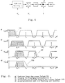
- FIG. 1 shows the basic circuit diagram of a digital AM residual sideband modulator according to the invention in the form of a double-balanced modulator M, which has the property of only generating the two sidebands without the original baseband video signal in the output spectrum.
- this digital mode of operation of a double push-pull modulator is shown schematically with a changeover switch S, with which the digital video signal supplied at the input E is alternately fed directly or inverted to the output A via an inverter J.
- the digital video signal is generated from the analog video signal in an A / D converter which is clocked at a sampling frequency f a or the digital video signal is directly generated in digital form at a sampling frequency f a and fed to the input E.
- the double push-pull modulator M is clocked at half the sampling frequency, ie its switch S is periodically switched between a and b in the cycle f a / 2, as is shown schematically in the switching scheme according to FIG. 1. From the relationship between the sampling of the video signal indicated schematically in Fig. 1 and this switching at half frequency of the switch S it follows that every second sample of the video signal is inverted, this corresponds to an amplitude modulation with the carrier frequency f a / 2 without this requires a correspondingly complex, digitally generated sine signal for the carrier, the modulation with the carrier is carried out only by switching the switch S. This results in a particularly simple structure. Theoretically, this mode of operation can be described by modulating the video signal with a carrier with half the sampling frequency. As a special feature, the two sidebands are symmetrical to the Nyquist frequency.
- FIG. 2 shows the implementation of this residual sideband filter with two low-pass filters TP1 and TP2
- FIG. 3 shows the associated diagram. That with the sampling frequency f a generated digital video signal u1 is fed to the low-pass filter TP1, which is also clocked at the sampling frequency f a .
- the filter characteristic of this low-pass filter TP1 is selected such that after the modulator M, in addition to the upper sideband, the frequency response of the lower sideband is also determined in a mirrored manner, as shown in FIG. 3b.
- the low-pass function of the low-pass filter TP1 is thus transformed into a high-pass characteristic.
- a second low-pass filter TP2 is arranged at the output of the modulator M and limits the upper sideband according to FIG. 3c in such a way that an asymmetrical residual sideband is produced.
- this second low-pass filter TP2 must act across the previous Nyquist frequency, a change in the sampling rate is necessary, for example a doubling of the sampling rate to 2f a .
- a circuit for inserting sample values of zero amplitude with the clock frequency 2f a is provided between the modulator M and the low pass filter TP2, so that virtually a data stream of twice the sampling frequency is produced.
- the low-pass filter TP2 can then be clocked at twice the sampling frequency 2f a .
- the double consideration of each sample value by repetition increases the power of the resulting signal, but in itself represents filtering that corresponds to a cosine-shaped frequency response with a single zero at the original sampling frequency f a .
- the second low-pass filter TP2 thus forms the upper sideband of the carrier-frequency video signal spectrum according to the video standard; together with the mirrored characteristic of the first low-pass filter TP1, a resulting bandpass results, the overall characteristics of which correspond to the prescribed residual sideband filter standard, the carrier frequency being f a / 2 (corresponds to the intermediate frequency 38.9 MHz of the residual sideband filter according to data sheet 341001). 3c with the carrier frequency f a / 2 is fed to a D / A converter according to FIG. 4 and disturbing harmonics are screened out via an analog low-pass filter TP3.
- the residual sideband signal according to FIG. 3d is generated with a relatively lower sampling frequency f a of only slightly more than twice the video bandwidth, it is also necessary to carry out an analog frequency conversion, for example to the standardized intermediate frequency of 38.9 MHz, according to Fig. 4, for example, with a mixer R, which is fed with a suitable carrier frequency F, a downstream bandpass filter BP1, the unused sidebands are filtered out.
- FIG. 5 shows the implementation with an upstream low-pass filter TP1 according to FIG. 2, but with a high-pass filter HP arranged after the modulator M.
- the necessary for this Analog low-pass post-filter TP3 must be implemented with a steeper filter flank, since the first harmonic band is closer to the useful band.
- FIG. 6 and 7 show the implementation of the digital filter directly as a bandpass filter BP2.
- This direct implementation of the filter as a bandpass filter assumes that its clock frequency is clocked again at twice the sampling frequency 2f a .
- the characteristic of the analog pre-filter is also shown here in the form of a low-pass filter TP4.
- the spectral representation according to FIG. 7 shows that the analog prefilter TP4 may allow band overlaps, ie at the Nyquist frequency f a / 2 no very high blocking attenuation is required. This property applies analogously when two low-pass filters are used for RSB bandpass implementation.
- the sampling frequency f a must be chosen to be greater than twice the bandwidth (2 ⁇ 5 MHz) of the video signal, on the other hand it should be as small as possible for reasons of cheap implementation. If the sampling frequency were chosen to be 20 MHz, for example, which corresponds to a carrier frequency of 10 MHz, then a sampling frequency of 40 MHz would be required for the second low-pass filter TP2 or bandpass filter BP2, which is difficult to achieve in conventional TTL technology. For this reason it is advantageous to use a sampling frequency below 25 MHz.
- the first possibility is to select the sampling frequency f a in accordance with the sampling frequency of 13.5 MHz, which is defined for the digitization of video signals according to CCIR standard 601. This is the invention Modulator directly compatible with external digital studio devices, a digital video signal generated according to the standard can be fed directly at input E of the modulator, an additional A / D converter is unnecessary.
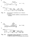
- the sampling frequency from other points of view, for example according to FIG. 8 such that the harmonic spectra arising during the modulation do not overlap the intended final carrier frequency spectrum after a final analog cooking mixture.
- the downstream D / A converter has a si-shaped post-filter effect, which normally has zeros in the sampling frequency and its multiples and which stands in the way of this advantageous utilization of the harmonics generated.
- Fig. 9 schematically shows this frequency response superimposed on the unevaluated scanning spectrum.
- This disruptive filter effect can be reduced by increasing the sampling frequency upstream of the D / A converter in conjunction with additionally inserted zero amplitudes between the actual sample values.This results in a pulse-amplitude-modulated output signal from a D / A converter with a smaller hold function, which has a weaker post-filter characteristic by shifting the zeros to higher frequencies, as shown in Figure 10.
- FIG. 12 shows how very advantageous frequency responses by increasing the clock frequency of the D.
- a purely digital modulator is to convert a COFDM-coded video signal present in the baseband from 0.4 to 8 MHz to the transmission frequency of an SFN transmitter, as is the case for processing the video signals in the individual transmitters of a single Frequency Network's is required.
- the COFDM-coded video signal which is supplied to all SFN transmitters, for example by a frequency-modulated satellite link, is digitally delayed via memory chains in a digital delay circuit, which operates with a sampling frequency f a of, for example, 20 MHz, and then in a modulator according to the invention with the aid of an intermediate frequency of, for example, 30 to 40 MHz is converted to the desired transmission frequency of the SFN transmitters.
- the corresponding time-delayed digital video signal with a carrier frequency of 10 MHz which is again half the sampling frequency f a in the delay circuit, is selected in the digital double push-pull modulator on the IF frequency implemented.
- the upper sideband between 30 and 40 MHz of the second repetition of the spectrum is filtered out as IF by digital filters. This can be done either by a bandpass with a 4-fold sampling frequency of 80 MHz or again by a low-pass filter with a sampling frequency of 20 MHz before the modulator and a low-pass filter with a 4-fold sampling frequency of 80 MHz after the modulator, as is shown in the previous figure is also described with respect to the residual sideband modulator.
- the IF signal is then converted to the actual transmission frequency of the SFN transmitter using a conventional analog mixer.
Abstract
Description
Die Erfindung betrifft einen Modulator zum Modulieren eines Trägers mit einem digitalen Videosignal.The invention relates to a modulator for modulating a carrier with a digital video signal.
In der Fernsehtechnik besteht in zunehmendem Maße Bedarf an Modulatoren, die digital arbeiten und damit unmittelbar digitale Videosignale umsetzen können.In television technology, there is an increasing need for modulators that work digitally and thus can directly convert digital video signals.
Zur Übertragung von Videosignalen wird beispielsweise die sogenannte Restseitenband-Amplitudenmodulation angewendet, bei der eines der entstehenden Seitenbänder vollständig und das andere Seitenband nur teilweise mit relativ langsam abfallender Amplitude nach höheren Modulationsfrequenzen hin übertragen wird (siehe beispielsweise Schönfelder, Nachrichtentechnik, Justus von Liebig Verlag, Darmstadt, Abschnitt IX oder Mäusl, Fernsehtechnik, Hüthig Buchverlag Heidelberg, Seiten 16 bis 19). Hierfür werden bisher ausschließlich analoge Modulatoren benutzt. Ein ähnliches Problem besteht bei einem Single-Frequency-Network (SFN), bei dem alle Sender ein identisches Signal zeitgleich abstrahlen. Um Laufzeitunterschiede der über Satelliten-Strecken übertragenen COFDM- (Coded-Orthogonal-Frequency-Division and Multiplexing) codierten Videosignale auszugleichen werden in jedem Sender digitale Verzögerungsschaltungen eingesetzt. Auch hier ist für die anschließende Umsetzung des im Basisband vorliegenden digitalen Videosignals auf die Sendefrequenz des SFN ein digitaler Modulator erforderlich.For the transmission of video signals, for example, the so-called residual sideband amplitude modulation is used, in which one of the resulting sidebands is transmitted completely and the other sideband is only partially transmitted with a relatively slowly falling amplitude after higher modulation frequencies (see, for example, Schönfelder, Kommunikationstechnik, Justus von Liebig Verlag, Darmstadt , Section IX or Mäusl, Fernsehtechnik, Hüthig Buchverlag Heidelberg, pages 16 to 19). So far, only analog modulators have been used for this. A similar problem exists with a single frequency network (SFN), in which all transmitters emit an identical signal at the same time. To transit time differences of the satellite-distances transmitted COFDM (C oded- O rthogonal- F requency- D ivision and Multiplexing) To compensate for coded video signals, digital delay circuits are used in every transmitter. A digital modulator is also required here for the subsequent conversion of the digital video signal present in the baseband to the transmission frequency of the SFN.
Es ist daher Aufgabe der Erfindung, einen Modulator zum Modulieren eines Trägers mit einem digitalen Videosignal zu schaffen, der digital arbeitet.It is therefore an object of the invention to provide a modulator for modulating a carrier with a digital video signal, which works digitally.
Diese Aufgabe wird durch einen Modulator laut Hauptanspruch gelöst. Vorteilhafte Weiterbildungen ergeben sich aus den Unteransprüchen.This task is solved by a modulator according to the main claim. Advantageous further developments result from the subclaims.
Durch die Verwendung eines Doppelgegentaktmodulators, der mit der halben Abtastfrequenz des zugeführten digitalen Videosignals getaktet wird, ergibt sich ein besonders einfacher Aufbau, da der Träger nicht als digitales Sinussignal aufbereitet werden muß, es genügt, den Umschalter des Doppelgegentaktmodulators im Takt der halben Abtastfrequenz umzuschalten. Die Trägerfrequenz entspricht dabei der halben Abtastfrequenz des Videosignals. Ein solcher Doppelgegentaktmodulator besitzt darüber hinaus noch die vorteilhafte Eigenschaft, daß nur noch die beiden AM-Seitenbänder ohne Träger entstehen und auch das ursprüngliche Basisband-Videosignal nicht mehr im Ausgangsspektrum erscheint. Lediglich eventuelle Gleichanteile im Videosignal (Grauwerte) erzeugen eine entsprechende Trägeramplitude. Im Ausgangssignal ist also das zu modulierende Videosignal nicht mehr additiv dem Trägerfrequenzsignal überlagert, dadurch ist es möglich, mit relativ einfachen digitalen Filtern das jeweils gewünschte modulierte Nutzsignal auszufiltern. Die Verwendung von digitalen Filtern ermöglicht einen besonders einfachen und preiswerten Aufbau eines Restseitenband-Modulators, da die nach der Fernsehnorm erforderlichen steilflankigen Restseitenbandfilter (beispielsweise nach CCIR-Norm und beschrieben im Datenblatt 341001 der Firma Rohde & Schwarz auf Seiten 10 und 11) mit nach der Norm vorgegebenen sehr engen Toleranzen in Digitaltechnik sehr exakt realisiert werden können. Bei Verwendung eines erfindungsgemäßen Modulators als Einseitenband-Modulator, wie dies bei den Sendern eines SFN zweckmäßig ist, werden entsprechend bemessene digitale Einseitenbandfilter eingesetzt. Für die Realisierung dieser Digitalfilter gibt es nach den Unteransprüchen verschiedene Möglichkeiten als Tiefpaß-, Hochpaß- bzw. Bandpaßfilter.The use of a double push-pull modulator, which is clocked at half the sampling frequency of the supplied digital video signal, results in a particularly simple structure, since the carrier does not have to be processed as a digital sine signal, it is sufficient to switch the switch of the double push-pull modulator at the clock of half the sampling frequency. The carrier frequency corresponds to half the sampling frequency of the video signal. Such a double push-pull modulator also has the advantageous property that only the two AM sidebands are produced without a carrier and the original baseband video signal no longer appears in the output spectrum. Only possible direct components in the video signal (gray values) generate a corresponding carrier amplitude. In the output signal, the video signal to be modulated is no longer additively superimposed on the carrier frequency signal possible to filter out the desired modulated useful signal with relatively simple digital filters. The use of digital filters enables a particularly simple and inexpensive construction of a residual sideband modulator, since the steep-sided residual sideband filters required by the television standard (for example, according to the CCIR standard and described in data sheet 341001 by Rohde & Schwarz on
Der erfindungsgemäße digitale Modulator besitzt darüber hinaus den besonderen Vorteil, daß für seinen Betrieb eine relativ niedrige Abtastfrequenz benutzt werden kann, an seine Verarbeitungsgeschwindigkeit also relativ geringe Ansprüche gestellt werden, so daß er mit den derzeit handelsüblichen digitalen Bauelementen einfach und preiswert realisiert werden kann. Es ist lediglich erforderlich, daß die gewählte Abtastfrequenz für das Videosignal, durch die gleichzeitig auch die Umschaltfrequenz des Doppelgegentaktmodulators bestimmt ist, größer als die doppelte Bandbreite des Videosignals (2 x 5 MHz) gewählt wird, nach oben hin besteht im Prinzip keine Beschränkung. Um jedoch mit möglichst geringer digitaler Arbeitsgeschwindigkeit auszukommen ist es vorteilhaft, die Abtastfrequenz kleiner als 20 MHz zu wählen. Verschiedene besonders vorteilhafte Bemessungsvorschriften für die Abtastfrequenz ergeben sich aus den Unteransprüchen. Wenn mit relativ niedriger Abtastfrequenz und damit auch Trägerfrequenz des Modulators gearbeitet wird, genügt es, mittels eines nachfolgenden üblichen analogen Mischers das digital erzeugte Restseitenbandsignal auf die gewünschte Ausgangsfrequenz, beispielsweise die derzeit übliche Zwischenfrequenz von 38,9 MHz hochzumischen.The digital modulator according to the invention also has the particular advantage that a relatively low sampling frequency can be used for its operation, so relatively low demands are placed on its processing speed, so that it can be implemented simply and inexpensively with the currently commercially available digital components. It is only necessary that the selected sampling frequency for the video signal, which also determines the switching frequency of the double-balanced modulator, is chosen to be greater than twice the bandwidth of the video signal (2 x 5 MHz), there is in principle no upper limit. However, in order to get by with the lowest possible digital working speed, it is essential advantageous to choose the sampling frequency less than 20 MHz. Various particularly advantageous design regulations for the sampling frequency result from the subclaims. When working with a relatively low sampling frequency and thus also the carrier frequency of the modulator, it suffices to use a subsequent conventional analog mixer to mix up the digitally generated residual sideband signal to the desired output frequency, for example the currently common intermediate frequency of 38.9 MHz.
Ein erfindungsgemäßer digitaler Modulator ist nicht nur sehr einfach und preiswert herstellbar, er besitzt gegenüber den bisher üblichen analogen Modulatoren auch noch den Vorteil, daß er in dem einmal gewählten Aufbau exakt reproduzierbar ist, keine Abgleicharbeiten erfordert und seine Charakteristik auch nicht durch Temperaturänderungen oder dergleichen beeinflußt wird.
Die Erfindung wird im folgenden anhand schematischer Zeichnungen an Ausführungsbeispielen eines Restseitenband-Modulators näher erläutert.A digital modulator according to the invention is not only very simple and inexpensive to produce, it also has the advantage over the conventional analog modulators that it can be reproduced exactly in the chosen structure, does not require any adjustment work and does not influence its characteristics by temperature changes or the like becomes.
The invention is explained in more detail below with the aid of schematic drawings using exemplary embodiments of a residual sideband modulator.
Fig. 1 zeigt das Prinzipschaltbild eines erfindungsgemäßen digitalen AM-Restseitenbandmodulators in Form eines Doppelgegentaktmodulators M, der die Eigenschaft besitzt, nur noch die beiden Seitenbänder ohne das ursprüngliche Basisband-Videosignal im Ausgangsspektrum zu erzeugen. In Fig. 1 ist diese digitale Wirkungsweise eines Doppelgegentaktmodulators schematisch mit einem Umschalter S dargestellt, mit welchem das am Eingang E zugeführte digitale Videosignal abwechselnd direkt bzw. über einen Inverter J invertiert dem Ausgang A zugführt wird. Das digitale Videosignal wird aus dem analog zugeführten Videosignal in einem A/D-Wandler erzeugt, der mit einer Abtastfrequenz fa getaktet ist oder das digitale Videosignal wird unmittelbar in digitaler Form erzeugt mit einer Abtastfrequenz fa dem Eingang E zugeführt. Der Doppelgegentaktmodulator M ist mit der halben Abtastfrequenz getaktet, d.h. sein Umschalter S wird im Takt fa/2 periodisch zwischen a und b umgeschaltet, wie dies schematisch in dem Umschaltschema nach Fig. 1 dargestellt ist. Aus der Beziehung zwischen der in Fig. 1 schematisch angedeuteten Abtastung des Videosignals und dieser mit halber Frequenz erfolgenden Umschaltung des Schalters S ergibt sich, daß jeder zweite Abtastwert des Videosignals invertiert wird, dies entspricht einer Amplitudenmodulation mit der Trägerfrequenz fa/2, ohne daß dazu ein entsprechend aufwendig digital erzeugtes Sinussignal für den Träger notwendig ist, die Modulation mit dem Träger erfolgt nur durch Umschaltung des Schalters S. Damit ergibt sich ein besonders einfacher Aufbau. Theoretisch läßt sich diese Wirkungsweise mit der Modulation des Videosignals mit einem Träger mit der halben Abtastfrequenz beschreiben. Als Besonderheit liegen die beiden Seitenbänder symmetrisch zur Nyquist-Frequenz.1 shows the basic circuit diagram of a digital AM residual sideband modulator according to the invention in the form of a double-balanced modulator M, which has the property of only generating the two sidebands without the original baseband video signal in the output spectrum. In Fig. 1 this digital mode of operation of a double push-pull modulator is shown schematically with a changeover switch S, with which the digital video signal supplied at the input E is alternately fed directly or inverted to the output A via an inverter J. The digital video signal is generated from the analog video signal in an A / D converter which is clocked at a sampling frequency f a or the digital video signal is directly generated in digital form at a sampling frequency f a and fed to the input E. The double push-pull modulator M is clocked at half the sampling frequency, ie its switch S is periodically switched between a and b in the cycle f a / 2, as is shown schematically in the switching scheme according to FIG. 1. From the relationship between the sampling of the video signal indicated schematically in Fig. 1 and this switching at half frequency of the switch S it follows that every second sample of the video signal is inverted, this corresponds to an amplitude modulation with the carrier frequency f a / 2 without this requires a correspondingly complex, digitally generated sine signal for the carrier, the modulation with the carrier is carried out only by switching the switch S. This results in a particularly simple structure. Theoretically, this mode of operation can be described by modulating the video signal with a carrier with half the sampling frequency. As a special feature, the two sidebands are symmetrical to the Nyquist frequency.
Um die bei der digitalen Modulation entstehende Doppelseitenband-AM in eine RSB-AM zu überführen sind dem Doppelgegentaktmodulator nach Fig. 1 noch zusätzliche digitale Filter zugeordnet, deren Amplitudencharakteristik den Restseitenbandfilter-Normvorschriften entsprechen. Fig. 2 zeigt die Realisierung dieses Restseitenbandfilters mit zwei Tiefpässen TP1 und TP2, Fig. 3 zeigt das zugehörige Diagramm. Das mit der Abtastfrequenz fa erzeugte digitale Videosignal u1 wird dem Tiefpaß TP1 zugeführt, der ebenfalls mit der Abtastfrequenz fa getaktet ist. Die Filtercharakteristik dieses Tiefpasses TP1 ist so gewählt, daß nach dem Modulator M neben dem oberen Seitenband auch der Frequenzgang des unteren Seitenbandes in gespiegelter Form bestimmt ist, wie dies Fig. 3b zeigt. Die Tiefpaßfunktion des Tiefpasses TP1 wird damit in eine Hochpaßcharakteristik transformiert. Am Ausgang des Modulators M ist ein zweiter Tiefpaß TP2 angeordnet, der das obere Seitenband gemäß Fig. 3c so begrenzt, daß ein unsymmetrisches Restseitenband entsteht. Da dieses zweite Tiefpaßfilter TP2 jedoch übergreifend über die bisherige Nyquist-Frequenz wirken muß, ist eine Abtastratenänderung erforderlich, beispielsweise eine Verdopplung der Abtastrate auf 2fa. Dazu ist gemäß Fig. 2 zwischen Modulator M und Tiefpaß TP2 eine Schaltung zum Einfügen von Abtastwerten der Amplitude Null mit der Taktfrequenz 2fa vorgesehen, so daß virtuell ein Datenstrom der doppelten Abtastfrequenz entsteht. Der Tiefpaß TP2 kann dann mit der doppelten Abtastfrequenz 2fa getaktet werden. Das zweifache Berücksichtigen jedes Abtastwertes durch Wiederholung erhöht zwar die Leistung des resultierenden Signals, stellt jedoch in sich bereits eine Filterung dar, die einem cosinusförmigen Frequenzgang mit einfacher Nullstelle bei der ursprünglichen Abtastfrequenz fa entspricht. Durch das zweite Tiefpaßfilter TP2 wird also das obere Seitenband des trägerfrequenten Videosignalspektrums nach der Videonorm geformt, zusammen mit der gespiegelten Charakteristik des ersten Tiefpasses TP1 ergibt sich ein resultierender Bandpaß, dessen Gesamtcharakteristik der vorgeschriebenen Restseitenbandfilter-Norm entspricht, wobei die Trägerfrequenz fa/2 ist (entspricht der Zwischenfrequenz 38,9 MHz der Restseitenbandfilter nach Datenblatt 341001). Das so digital erzeugte digitale Restseitenbandsignal gemäß Fig. 3c mit der Trägerfrequenz fa/2 wird gemäß Fig. 4 einem D/A-Wandler zugeführt und über ein analoges Tiefpaßfilter TP3 werden störende Oberwellen abgesiebt.In order to convert the double sideband AM arising in the digital modulation into an RSB-AM, additional double filters are assigned to the double push-pull modulator according to FIG. 1, the amplitude characteristics of which correspond to the residual sideband filter standard regulations. FIG. 2 shows the implementation of this residual sideband filter with two low-pass filters TP1 and TP2, FIG. 3 shows the associated diagram. That with the sampling frequency f a generated digital video signal u1 is fed to the low-pass filter TP1, which is also clocked at the sampling frequency f a . The filter characteristic of this low-pass filter TP1 is selected such that after the modulator M, in addition to the upper sideband, the frequency response of the lower sideband is also determined in a mirrored manner, as shown in FIG. 3b. The low-pass function of the low-pass filter TP1 is thus transformed into a high-pass characteristic. A second low-pass filter TP2 is arranged at the output of the modulator M and limits the upper sideband according to FIG. 3c in such a way that an asymmetrical residual sideband is produced. However, since this second low-pass filter TP2 must act across the previous Nyquist frequency, a change in the sampling rate is necessary, for example a doubling of the sampling rate to 2f a . For this purpose, according to FIG. 2, a circuit for inserting sample values of zero amplitude with the
Der Tiefpaß TP1 muß eine Durchlaßcharakteristik von 0 bis fg1 bei entsprechender Welligkeit des zu realisierenden Bandpasses (RSB-Filtertoleranz) aufweisen, so daß sich hierfür eine untere Bandpaßgrenzfrequenz von ![]()
![]()
![]()
![]()
Da in diesem Beispiel das Restseitenbandsignal nach Fig. 3d mit relativ niedrigerer Abtastfrequenz fa von nur etwas mehr als der doppelten Videobandbreite erzeugt wird ist es nötig, zusätzlich noch eine analoge Frequenzumsetzung beispielsweise auf die genormte Zwischenfrequenz von 38,9 MHz vorzunehmen, dies geschieht gemäß Fig. 4 beispielsweise mit einem Mischer R, der mit einer geeigneten Trägerfrequenz F gespeist ist, über ein nachgeschaltetes Bandpaßfilter BP1 werden die nicht benutzten Seitenbänder weggefiltert.Since in this example the residual sideband signal according to FIG. 3d is generated with a relatively lower sampling frequency f a of only slightly more than twice the video bandwidth, it is also necessary to carry out an analog frequency conversion, for example to the standardized intermediate frequency of 38.9 MHz, according to Fig. 4, for example, with a mixer R, which is fed with a suitable carrier frequency F, a downstream bandpass filter BP1, the unused sidebands are filtered out.
Fig. 5 zeigt die Realisierung mit einem vorgeschalteten Tiefpaß TP1 gemäß Fig. 2, jedoch mit einem nach dem Modulator M angeordneten Hochpaß HP. Das hierfür notwendige analoge Tiefpaß-Nachfilter TP3 muß hier mit einer steileren Filterflanke realisiert werden, da das erste Oberwellenband näher am Nutzband liegt.FIG. 5 shows the implementation with an upstream low-pass filter TP1 according to FIG. 2, but with a high-pass filter HP arranged after the modulator M. The necessary for this Analog low-pass post-filter TP3 must be implemented with a steeper filter flank, since the first harmonic band is closer to the useful band.
Fig. 6 und 7 zeigen die Realisierung des digitalen Filters unmittelbar als Bandpaß BP2. Diese direkte Realisierung des Filters als Bandpaß setzt voraus, daß dessen Taktfrequenz wieder mit der doppelten Abtastfrequenz 2fa getaktet wird. Außerdem ist hier die Charakteristik des analogen Vorfilters in Form eines Tiefpasses TP4 dargestellt. Die Spektraldarstellung nach Fig. 7 zeigt, daß das analoge Vorfilter TP4 Bandüberlappungen zulassen darf, d.h. bei der Nyquist-Frequenz fa/2 ist noch keine sehr hohe Sperrdämpfung zu fordern. Diese Eigenschaft gilt analog bei der Verwendung zweier Tiefpässe zur RSB-Bandpaßrealisierung.6 and 7 show the implementation of the digital filter directly as a bandpass filter BP2. This direct implementation of the filter as a bandpass filter assumes that its clock frequency is clocked again at twice the
Wie sich aus den Spektrumsdarstellungen ergibt, muß die Abtastfrequenz fa größer als die doppelte Bandbreite (2 x 5 MHz) des Videosignals gewählt werden, andererseits soll sie aus Gründen der billigen Realisierbarkeit möglichst klein sein. Würde die Abtastfrequenz beispielsweise zu 20 MHz gewählt, was einer Trägerfrequenz von 10 MHz entspricht, so wäre für den zweiten Tiefpaß TP2 bzw. Bandpaß BP2 eine Abtastfrequenz von 40 MHz erforderlich, was in üblicher TTL-Technik nur schwer zu realisieren ist. Aus diesem Grunde ist es vorteilhaft, eine Abtastfrequenz unter 25 MHz zu benutzen. Als erste Möglichkeit bietet sich an, die Abtastfrequenz fa entsprechend der für die Digitalisierung von Videosignalen nach CCIR-Norm 601 festgelegten Abtastfrequenz von 13,5 MHz zu wählen. Damit ist der erfindungsgemäße Modulator mit externen digitalen Studiogeräten unmittelbar kompatibel, ein nach der Norm erzeugtes digitales Videosignal kann unmittelbar am Eingang E des Modulators eingespeist werden, ein zusätzlicher A/D-Wandler ist überflüssig.As can be seen from the spectrum representations, the sampling frequency f a must be chosen to be greater than twice the bandwidth (2 × 5 MHz) of the video signal, on the other hand it should be as small as possible for reasons of cheap implementation. If the sampling frequency were chosen to be 20 MHz, for example, which corresponds to a carrier frequency of 10 MHz, then a sampling frequency of 40 MHz would be required for the second low-pass filter TP2 or bandpass filter BP2, which is difficult to achieve in conventional TTL technology. For this reason it is advantageous to use a sampling frequency below 25 MHz. The first possibility is to select the sampling frequency f a in accordance with the sampling frequency of 13.5 MHz, which is defined for the digitization of video signals according to CCIR standard 601. This is the invention Modulator directly compatible with external digital studio devices, a digital video signal generated according to the standard can be fed directly at input E of the modulator, an additional A / D converter is unnecessary.
In manchen Anwendungfällen kann es vorteilhaft sein, die Abtastfrequenz nach anderen Gesichtspunkten zu wählen, beispielsweise gemäß Fig. 8 so, daß die bei der Modulation entstehenden Oberwellenspektren nicht das vorgesehene endgültige Trägerfrequenzspektrum nach einer abschließenden analogen Kochmischung überlagern. Ist beispielsweise die Erzeugung eines endgültigen Trägerfrequenzspektrums in der genormten ZF-Lage mit einem Träger von 38,9 MHz gewünscht, so wird gemäß Fig. 8 mit einer Abtastfrequenz fa = 12,3 MHz ein Oberwellenspektrum erzeugt, das in der gewünschten in Fig. 8 schraffiert dargestellten Trägerfrequenzlage frei ist und das gemäß Fig. 4 auf 38,9 MHz hochgemischte Trägerfrequenzspektrum also nicht durch Oberwellen des Modulationsspektrums gestört ist.In some applications it may be advantageous to choose the sampling frequency from other points of view, for example according to FIG. 8 such that the harmonic spectra arising during the modulation do not overlap the intended final carrier frequency spectrum after a final analog cooking mixture. If, for example, the generation of a final carrier frequency spectrum in the standardized IF position with a carrier of 38.9 MHz is desired, a harmonic spectrum is generated in accordance with FIG. 8 with a sampling frequency f a = 12.3 MHz, which in the desired in FIG. 8 hatched carrier frequency position is free and the carrier frequency spectrum which is highly mixed according to FIG. 4 to 38.9 MHz is not disturbed by harmonics of the modulation spectrum.
Eine andere Möglichkeit ist, die Taktfrequenz fa entsprechend einer gewünschten endgültigen Trägerfrequenz zu wählen. Besonders günstig sind hierbei ganzzahlige Verhältnisse. Zur Modulation eines Videosignals auf die Norm-ZF von 38,9 MHz bietet sich beispielsweise eine Abtastfrequenz von 1/3 x 38,9 = 12,97 MHz an. Durch eine phasenstarre Verkopplung werden Störungen durch Oberwellen praktisch nicht wirksam. Anders herum kann ausgehend von einer vorher festgelegten Abtastfrequenz von z.B. 13,5 MHz eine modifizierte gewünschte Trägerlage von z.B. 3 x 13,5 = 40,5 MHz gewählt werden.Another possibility is to choose the clock frequency f a in accordance with a desired final carrier frequency. Integer ratios are particularly favorable here. For example, a sampling frequency of 1/3 x 38.9 = 12.97 MHz is suitable for modulating a video signal to the standard IF of 38.9 MHz. Due to a phase-locked coupling, interference from harmonics is practically ineffective. Conversely, a modified desired carrier position of, for example, 3 x 13.5 = 40.5 MHz can be selected on the basis of a previously determined sampling frequency of, for example, 13.5 MHz.
Ein weiterer Vorteil des erfindungsgemäßen digitalen Modulators besteht darin, gezielt die bei der Modulation entstehenden Oberwellenbänder für die Erzeugung des gewünschten Trägerfrequenzspektrums auszunutzen, die hinter dem D/A-Wandler nach dem Modulator vorhanden sind. Wenn beispielsweise gemäß Fig. 3c die Taktfrequenz fa so gewählt wird, daß das bei 5fa/2 entstehende Oberwellenspektrum mit der gewünschten Trägerfrequenz übereinstimmt, kann dieses Spektrum 5fa/2 hinter dem D/A-Wandler unmittelbar mit einem entsprechend dimensionierten Bandpaß ausgesiebt werden. Ist beispielsweise eine endgültige Trägerfrequenzlage für das Nutzspektrum bei 38,9 MHz erwünscht, so wird dies mit einer Abtastfrequenz fa = 38,9 : 2,5 = 15,56 MHz erreicht.A further advantage of the digital modulator according to the invention is to specifically use the harmonic bands which arise during the modulation for the generation of the desired carrier frequency spectrum and which are present behind the D / A converter after the modulator. If, for example, according to FIG. 3c, the clock frequency f a is selected so that the harmonic spectrum arising at 5f a / 2 matches the desired carrier frequency, this
Der nachgeschaltete D/A-Wandler besitzt eine si-förmige Nachfilterwirkung, die normalerweise Nullstellen bei der Abtastfrequenz und ihren Vielfachen aufweist und die dieser vorteilhaften Ausnutzung der erzeugten Oberwellen entgegensteht. Fig.9 zeigt schematisch diesen Frequenzgang in Überlagerung zum unbewerteten Abtastspektrum. Diese störende Filterwirkung kann durch eine Erhöhung der Abtastfrequenz vor dem D/A-Wandler in Verbindung mit zusätzlich eingefügten Nullamplituden zwischen den eigentlichen Abtastwerten verringert werden, dadurch wird ein pulsamplitudenmoduliertes Ausgangssignal eines D/A-Wandlers mit kleinerer Haltefunktion erreicht, die eine schwächere Nachfiltereigenschaft besitzt, indem die Nullstellen zu höheren Frequenzen hin verschoben werden, wie dies Bild 10 zeigt.The downstream D / A converter has a si-shaped post-filter effect, which normally has zeros in the sampling frequency and its multiples and which stands in the way of this advantageous utilization of the harmonics generated. Fig. 9 schematically shows this frequency response superimposed on the unevaluated scanning spectrum. This disruptive filter effect can be reduced by increasing the sampling frequency upstream of the D / A converter in conjunction with additionally inserted zero amplitudes between the actual sample values.This results in a pulse-amplitude-modulated output signal from a D / A converter with a smaller hold function, which has a weaker post-filter characteristic by shifting the zeros to higher frequencies, as shown in Figure 10.
Zusätzlich zu dieser Erhöhung der Taktfrequenz kann gemäß Fig. 11 vor dem D/A-Wandler ein mit der gleichen erhöhten Taktfrequenz getaktetes digitales Hochpaßfilter HP1 vorgesehen werden, hierdurch wird die Signalenergie des gewünschten Spektrums angehoben. Fig. 12 zeigt, wie auf diese Weise beispielsweise durch ein sogenanntes (1-1)-Hochpaßfilter (Fig. 12a) bzw. ein sogenanntes digitales (-1/2/-1)-Filter sehr vorteilhafte Frequenzgänge durch Erhöhung der Taktfrequenz des D/A-Wandlers erzeugt werden können und zwar durch Vervierfachung der Taktfrequenz für den D/A-Wandler und auch für den Hochpaß HP1 (n = 4).In addition to this increase in the clock frequency, a digital high-pass filter HP1 clocked with the same increased clock frequency can be provided in front of the D / A converter, as a result of which the signal energy of the desired spectrum is increased. FIG. 12 shows how very advantageous frequency responses by increasing the clock frequency of the D. By using a so-called (1-1) high-pass filter (FIG. 12a) or a so-called digital (-1 / 2 / -1) filter / A converter can be generated by quadrupling the clock frequency for the D / A converter and also for the high pass HP1 (n = 4).
Eine andere Anwendungsmöglichkeit für einen erfindungsgemäßen rein digital arbeitenden Modulator besteht bei der Umsetzung eines im Basisband von 0,4 bis 8 MHz vorliegenden COFDM-codierten Videosignals auf die Sendefrequenz eines SFN-Senders, wie dies zur Aufbereitung der Videosignale in den einzelnen Sendern eines Single-Frequency-Network's erforderlich ist. Hier wird das COFDM-codierte Videosignal, das beispielsweise durch eine frequenzmodulierte Satellitenstrecke allen SFN-Sendern zugeführt wird, in einer digitalen Verzögerungsschaltung, die mit einer Abtastfrequenz fa von beispielsweise 20 MHz arbeitet, über Speicherketten digital verzögert und anschließend in einem erfindungsgemäßen Modulator mit Hilfe einer Zwischenfrequenz von z.B. 30 bis 40 MHz auf die gewünschte Sendefrequenz der SFN-Sender umgesetzt. Dazu wird im digitalen Doppel-Gegentakt-Modulator das entsprechend zeitverzögerte digitale Videosignal mit einer Trägerfrequenz von 10 MHz, die also wieder halb so groß wie die Abtastfrequenz fa in der Verzögerungsschaltung gewählt ist, auf die ZF-Frequenz umgesetzt. Durch digitale Filter wird das obere Seitenband zwischen 30 und 40 MHz der zweiten Wiederholung des Spektrums als ZF herausgefiltert. Dies kann entweder durch einen Bandpaß mit einer 4-fachen Abtastfrequenz von 80 MHz durchgeführt werden oder wieder durch einen Tiefpaß mit einer Abtastfrequenz von 20 MHz vor dem Modulator und einem Tiefpaß mit der 4-fachen Abtastfrequenz von 80 MHz nach dem Modulator, wie dies anhand der vorhergehenden Fig. auch bezüglich des Restseitenband-Modulators beschrieben ist. Das ZF-Signal wird dann mit einem üblichen analogen Mischer auf die eigentliche Sendefrequenz des SFN-Senders umgesetzt.Another possible application for a purely digital modulator according to the invention is to convert a COFDM-coded video signal present in the baseband from 0.4 to 8 MHz to the transmission frequency of an SFN transmitter, as is the case for processing the video signals in the individual transmitters of a single Frequency Network's is required. Here, the COFDM-coded video signal, which is supplied to all SFN transmitters, for example by a frequency-modulated satellite link, is digitally delayed via memory chains in a digital delay circuit, which operates with a sampling frequency f a of, for example, 20 MHz, and then in a modulator according to the invention with the aid of an intermediate frequency of, for example, 30 to 40 MHz is converted to the desired transmission frequency of the SFN transmitters. For this purpose, the corresponding time-delayed digital video signal with a carrier frequency of 10 MHz, which is again half the sampling frequency f a in the delay circuit, is selected in the digital double push-pull modulator on the IF frequency implemented. The upper sideband between 30 and 40 MHz of the second repetition of the spectrum is filtered out as IF by digital filters. This can be done either by a bandpass with a 4-fold sampling frequency of 80 MHz or again by a low-pass filter with a sampling frequency of 20 MHz before the modulator and a low-pass filter with a 4-fold sampling frequency of 80 MHz after the modulator, as is shown in the previous figure is also described with respect to the residual sideband modulator. The IF signal is then converted to the actual transmission frequency of the SFN transmitter using a conventional analog mixer.
Claims (16)
Applications Claiming Priority (2)
| Application Number | Priority Date | Filing Date | Title |
|---|---|---|---|
| DE19944426935 DE4426935A1 (en) | 1994-07-29 | 1994-07-29 | Digital residual sideband modulator for video signals |
| DE4426935 | 1994-07-29 |
Publications (2)
| Publication Number | Publication Date |
|---|---|
| EP0695066A2 true EP0695066A2 (en) | 1996-01-31 |
| EP0695066A3 EP0695066A3 (en) | 1999-08-11 |
Family
ID=6524463
Family Applications (1)
| Application Number | Title | Priority Date | Filing Date |
|---|---|---|---|
| EP95108686A Withdrawn EP0695066A3 (en) | 1994-07-29 | 1995-06-07 | Digital modulator for video signals |
Country Status (2)
| Country | Link |
|---|---|
| EP (1) | EP0695066A3 (en) |
| DE (1) | DE4426935A1 (en) |
Cited By (1)
| Publication number | Priority date | Publication date | Assignee | Title |
|---|---|---|---|---|
| EP0876077A2 (en) * | 1997-04-18 | 1998-11-04 | Alcatel | Method and apparatus for addition of signals existing as sampling values |
Families Citing this family (1)
| Publication number | Priority date | Publication date | Assignee | Title |
|---|---|---|---|---|
| DE102007001281B4 (en) | 2007-01-08 | 2018-10-18 | Rohde & Schwarz Gmbh & Co. Kg | Electronic measuring device with switchable trigger filter |
Family Cites Families (5)
| Publication number | Priority date | Publication date | Assignee | Title |
|---|---|---|---|---|
| GB1432373A (en) * | 1972-08-15 | 1976-04-14 | Indep Broadcasting Authority | Apparatus for producing digised signals for defining an amplitude modulated sub-carrier |
| NL168099C (en) * | 1974-09-12 | 1982-02-16 | Philips Nv | MODULATION AND FILTER DEVICE FOR DIGITAL SIGNALS. |
| GB2219906A (en) * | 1988-06-15 | 1989-12-20 | Sony Corp | Image data transmitting systems |
| US4973977A (en) * | 1988-11-29 | 1990-11-27 | Comlux | Digital to amplitude modulated analog converter |
| FR2689350B1 (en) * | 1992-03-30 | 1995-04-21 | France Telecom | Amplitude modulator with residual sideband for sampled or digital analog signals and its use in television. |
-
1994
- 1994-07-29 DE DE19944426935 patent/DE4426935A1/en not_active Withdrawn
-
1995
- 1995-06-07 EP EP95108686A patent/EP0695066A3/en not_active Withdrawn
Non-Patent Citations (2)
| Title |
|---|
| MAEUSL: "Fernsehtechnik", HUETHIG BUCHVERLAG, HEIDELBERG, pages: 16 - 19 |
| SCHOENFELDER: "Nachrichrentechnik", JUSTUS VON LIEBIG VERLAG, DARMSTADT |
Cited By (3)
| Publication number | Priority date | Publication date | Assignee | Title |
|---|---|---|---|---|
| EP0876077A2 (en) * | 1997-04-18 | 1998-11-04 | Alcatel | Method and apparatus for addition of signals existing as sampling values |
| EP0876077A3 (en) * | 1997-04-18 | 2001-02-07 | Alcatel | Method and apparatus for addition of signals existing as sampling values |
| US6272181B1 (en) | 1997-04-18 | 2001-08-07 | Alcatel | Method and device for the aggregation of signals from sampling values |
Also Published As
| Publication number | Publication date |
|---|---|
| DE4426935A1 (en) | 1996-02-01 |
| EP0695066A3 (en) | 1999-08-11 |
Similar Documents
| Publication | Publication Date | Title |
|---|---|---|
| DE69530214T2 (en) | RECEIVER WITH SQUARE DECIMATION LEVEL AND METHOD FOR PROCESSING DIGITAL SIGNALS | |
| EP1657917B1 (en) | Method and circuit arrangement for filtering analog or digital modulated TV signals | |
| WO1986002505A1 (en) | Process and circuit arrangement for converting frequency-modulated signals through at least one intermediate frequency into low-frquency signals | |
| DE4337135C1 (en) | Drop-and-add multiplexer for converting and conditioning a frequency-division multiplex signal | |
| DE2703566B2 (en) | Frequency modulation system | |
| DE1816033B2 (en) | SENDING DEVICE FOR TRANSMISSION OF PULSES | |
| EP0695066A2 (en) | Digital modulator for video signals | |
| DE2608939C3 (en) | mixer | |
| EP0651526A2 (en) | Method for processing a digital frequencymultiplex signal | |
| DE2730153A1 (en) | Radio signals reception by frequency changing method - involves input signal division between two signal paths, and mixing with oscillator signals whose phases differ by 180 degrees | |
| DE102005046398B3 (en) | HF-input signal e.g. frequency-modulated signal, processing circuit, has frequency divider that divides intermediate frequency so that reduced and scanning frequencies are spaced apart to fulfill scanning theorem with reduced frequency | |
| DE2802938B2 (en) | Frequency band dividing filter | |
| AT214988B (en) | Device for converting a color television signal of a certain standard into a signal of another standard | |
| DE19731012B4 (en) | Arrangement for generating a vestigial sideband modulated video signal with residual carrier for a television station | |
| DE3346059A1 (en) | FM STEREO RECEIVER | |
| DE3922999C2 (en) | Intermediate audio frequency converter | |
| EP0369102B1 (en) | Modulation method and arrangement for carrying out the method | |
| WO2001015432A2 (en) | Method for the signal conversion of a modulated real-value analogue image signal and corresponding signal conversion | |
| EP0834228A1 (en) | Frequency- and phase-regulator circuit for vsb receivers | |
| DE19628996A1 (en) | Circuit arrangement for frequency conversion of a color signal | |
| EP0109963B1 (en) | Device for editing picture carriers of television signals | |
| DE3918530A1 (en) | Optical cable TV transmission system | |
| DE3344318C1 (en) | Frequency converter with a circuit arrangement for suppressing an oscillator signal in the output signal of a mixer | |
| DE2715834A1 (en) | Single side-band wave generation system - has two oscillators producing IF wave to generate carrier wave which is modulated with AF | |
| DE3741610A1 (en) | Arrangement for demodulating single-sideband signals |
Legal Events
| Date | Code | Title | Description |
|---|---|---|---|
| PUAI | Public reference made under article 153(3) epc to a published international application that has entered the european phase |
Free format text: ORIGINAL CODE: 0009012 |
|
| AK | Designated contracting states |
Kind code of ref document: A2 Designated state(s): DE FR GB IT |
|
| PUAL | Search report despatched |
Free format text: ORIGINAL CODE: 0009013 |
|
| AK | Designated contracting states |
Kind code of ref document: A3 Designated state(s): DE FR GB IT |
|
| RIC1 | Information provided on ipc code assigned before grant |
Free format text: 6H 04L 27/04 A, 6H 04N 7/24 B |
|
| 17P | Request for examination filed |
Effective date: 20000210 |
|
| STAA | Information on the status of an ep patent application or granted ep patent |
Free format text: STATUS: THE APPLICATION IS DEEMED TO BE WITHDRAWN |
|
| 18D | Application deemed to be withdrawn |
Effective date: 20030204 |