EP0695031A2 - Mobile communication device having an output power sensor succeeding a transmission filter - Google Patents
Mobile communication device having an output power sensor succeeding a transmission filter Download PDFInfo
- Publication number
- EP0695031A2 EP0695031A2 EP95111525A EP95111525A EP0695031A2 EP 0695031 A2 EP0695031 A2 EP 0695031A2 EP 95111525 A EP95111525 A EP 95111525A EP 95111525 A EP95111525 A EP 95111525A EP 0695031 A2 EP0695031 A2 EP 0695031A2
- Authority
- EP
- European Patent Office
- Prior art keywords
- output power
- signal
- antenna
- filter
- frequency band
- Prior art date
- Legal status (The legal status is an assumption and is not a legal conclusion. Google has not performed a legal analysis and makes no representation as to the accuracy of the status listed.)
- Granted
Links
Images


Classifications
-
- H—ELECTRICITY
- H04—ELECTRIC COMMUNICATION TECHNIQUE
- H04B—TRANSMISSION
- H04B7/00—Radio transmission systems, i.e. using radiation field
- H04B7/24—Radio transmission systems, i.e. using radiation field for communication between two or more posts
- H04B7/26—Radio transmission systems, i.e. using radiation field for communication between two or more posts at least one of which is mobile
-
- H—ELECTRICITY
- H03—ELECTRONIC CIRCUITRY
- H03G—CONTROL OF AMPLIFICATION
- H03G3/00—Gain control in amplifiers or frequency changers
- H03G3/20—Automatic control
- H03G3/30—Automatic control in amplifiers having semiconductor devices
- H03G3/3036—Automatic control in amplifiers having semiconductor devices in high-frequency amplifiers or in frequency-changers
- H03G3/3042—Automatic control in amplifiers having semiconductor devices in high-frequency amplifiers or in frequency-changers in modulators, frequency-changers, transmitters or power amplifiers
Definitions
- the present invention relates to a mobile communication device, and output power control circuitry and duplexer applicable thereto.
- a power amplifier amplifies the power of a signal to be transmitted, i.e., a carrier modulated by a speech signal or similar signal.
- the amplified signal is delivered to a transmitter filter (TX filter) via a first radio frequency signal path.
- TX filter limits the input signal to a predetermined frequency band for transmission.
- the output of the TX filter is routed through a branching circuit, which isolates a transmission section and a receipt section, and a second radio frequency signal path to an antenna.
- a branching circuit which isolates a transmission section and a receipt section, and a second radio frequency signal path to an antenna.
- a coupler is inserted in the first radio frequency signal path.
- the coupler produces part of the output signal of the power amplifier from the above path.
- the produced signal (part of the power amplifier output) is fed from the coupler to an automatic power control (APC) circuit in the form of an electric signal.
- APC automatic power control
- a controller controlling the entire mobile phone, feeds to the APC circuit a reference signal indicative of power to be output from the mobile phone and matching the current distance between the mobile phone and a base station.
- the APC circuit compares the produced signal and the reference signal and thereby generates a gain control signal for matching the former to the latter.
- the gain control signal from the APC circuit is applied to the power amplifier so as to stabilize the output power of the power amplifier at a predetermined value.
- TX filter and branching circuit are constructed into a single unit or part together with a receiver filter (RX filter) and are put on the market as a duplexer.
- RX filter receiver filter
- the conventional output power control circuitry is capable of controlling the output signal of the power amplifier to a preselected size, as stated above.
- the conventional circuitry has the following problem left unsolved.
- the TX filter is located to follow the power amplifier and closer to the antenna than the amplifier. In this condition, the output power of the TX filter and, therefore, that of the antenna has a frequency characteristic which is not flat due to the influence of the pass band deviation and low return loss of the TX filter.
- the words "pass band deviation" should be understood, throughout the following description, to refer to the fact that the attenuation factor of the TX filter, implemented by a band-pass filter, varies with frequencies lying in the pass band of the filter. Because the frequency of the signal to be transmitted corresponds to a channel currently occupied for transmission, the above problem means that the output power differs from one channel to another channel for transmission.
- TX filter For example, a certain kind of mobile phone available today must match itself to a great number of transmission channels having a carrier frequency range of from 824 MHz to 849 MHz.
- the TX filter is, therefore, required to have a pass band as broad as 25 MHz.
- the TX filter should discriminate frequencies with high accuracy at the boundaries between its pass band and the outside of the same. Consequently, some degree of pass band deviation is not avoidable in the TX filter.
- an object of the present invention to provide a mobile communication device capable of maintaining, despite the pass band deviation and low return loss of a TX filter, the output power of a signal to be transmitted constant without regard to the frequency of the signal.
- a mobile communication device has a power amplifier for amplifying the power of a signal to be transmitted, a TX filter for limiting the frequency band of the signal amplified by the power amplifier to a predetermined frequency band for transmission, an antenna for radiating the signal limited in frequency band by the TX filter to the air, and output power control circuitry for controlling the output power of the signal to be transmitted.
- the output power control circuitry has an output power sensor succeeding the TX filter in the direction of flow of the signal to be transmitted, and for sensing the output power of the signal, and an automatic power control circuit for controlling the gain of the power amplifier such that the output power sensed by the output power sensor coincides with a predetermined reference value.
- output power control circuitry for a mobile communication device which amplifies the power of a signal to be transmitted by a power amplifier, limits the frequency band of the signal amplified by the power amplifier to a predetermined frequency band for transmission by a TX filter, and transmits the signal lying in the predetermined frequency band via an antenna has an output power sensor succeeding the TX filter in the direction of flow of the signal to be transmitted, and for sensing the output power of the signal.
- An automatic power control circuit controls the gain of the power amplifier such that the output power sensed by the output power sensor coincides with a predetermined reference value.
- a duplexer has a TX filter for limiting the frequency band of a signal to be fed to an antenna to a predetermined frequency band for transmission.
- a RX filter separates from a signal coming in through the antenna the frequency components lying in a predetermined frequency band for receiving.
- a branching circuit isolates the TX filter and the RX filter connected to the antenna.
- An output power sensor is provided on a transmission path included in the branching circuit, and senses the output power of the signal to be fed to the antenna.
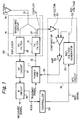
- a mobile communication device embodying the present invention is shown.
- the device has a power amplifier 11 forming part of a transmission section and connected to a duplexer 20 by a first radio frequency signal line 12.
- a radio frequency (RF) circuit 41 and an intermediate frequency (IF) circuit 42 form part of a receiving section.
- An antenna 16 is connected to the duplexer 20 by a second radio frequency signal line 15.
- An automatic power control (APC) circuit 18 controls the gain of the power amplifier 11, as will be described specifically later.
- a controller 50 controls the various constituents of the device. For example, when the controller 50 receives a received signal strength indication (RSSI) from the IF circuit 42, it generates a reference signal 51 for generating a reference voltage and feeds it to the APC circuit 18.
- RSSI received signal strength indication
- the duplexer 20 is made up of a TX filter 13, a RX filter 19, a branching circuit 14, and a coupler 17. These constituents 13, 19, 14 and 17 of the duplexer 20 are constructed into a single unit or part.
- the branching circuit 14 isolates the transmission section and the receiving section of the device from each other.
- the coupler 17 and APC circuit 18 constitute output power control circuitry in combination.
- FIG. 1 there are not shown the parts of the device not relevant to the understanding of the present invention. These parts include a circuit for modulating a carrier with a speech signal to thereby generate a signal to be transmitted, a circuit for demodulating a received signal, a dialing section, a display for displaying a telephone number and other necessary information, a speaker, and a microphone.
- the signal to be transmitted is amplified by the power amplifier 11 and then applied to the TX filter 13.
- the TX filter 13 limits the input signal to a predetermined frequency band for transmission.
- the output of the TX filter 13 is routed through the branching circuit 14 and radio frequency signal line 15 to the antenna 16 and radiated from the antenna 16 to the air as an electromagnetic wave.
- a signal coming in through the antenna 16 is applied to the RX filter 19 via the branching circuit 14.
- the RX filter 19 separates only the signal components lying in a predetermined frequency band for receiving.
- the resulting output of the RX filter 19 is amplified by the RF circuit 41 and then transformed to a first intermediate frequency (first IF).
- the IF circuit 42 receives the first IF from the RF circuit 41 and transforms it to a second intermediate frequency (second IF).
- the IF circuit 42 delivers to the controller 50 the signal not transformed to the second IF as the previously mentioned RSSI.
- the illustrative embodiment differs from the conventional device in respect of a control loop for controlling the output power.
- the coupler 17, playing the role of an output power sensor is inserted in a radio frequency path 21 included in the branching circuit 14 and assigned to transmission.
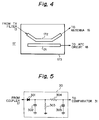
- the coupler 17 has a dielectric substrate 173 and two conductors 171 and 172 provided on the substrate 173.
- the coupler 17 serves as a side-coupling directional coupler.
- the coupler 17 produces part of the output signal of the TX filter 13 from the radio frequency path 21 and delivers it to the APC circuit 18 in the form of an electric signal.
- the reference signal 51 is applied from the controller 50 to the APC circuit 18, as stated earlier.
- the APC circuit 18 generates, based on the output of the coupler 17 and reference signal 51, a gain control signal for matching the power of the output of the TX filter 13 to the reference signal 51.
- the gain control signal is fed to the power amplifier 11.
- the coupler 17 is a specific form of an output power sensor and may be replaced with, for example, a branch line, it is more desirable than the others because it scarcely affects the transmission of a signal.
- the coupler 17 disposed in the branching circuit 17 forms part of the duplexer 20 together with the TX filter 13, branching circuit 14, and RX filter 19.
- the APC circuit 18 has a detector 30, a comparator 32, and a reference voltage generator 33.
- the detector 30 detects the output of the coupler 17 and generates a detection voltage (DC voltage) representative of its mean level.
- the detection signal from the detector 30 is fed to the comparator 31. Because the coupler 17 is disposed in the branching circuit 14, it produces even part of the reflected signal from the radio frequency path 21. However, this part is far lower in level than the produced part of the signal to be transmitted. Therefore, the detection voltage can be freed from the influence of the reflected signal if the sensitivity of the coupler 17 and that of the detector 30 are selected adequately.
- FIG. 5 shows a specific arrangement of the detector 30.
- the detector 30 has a diode 301, capacitors 302 and 305, and resistors 303 and 304. With these constituents, the detector 30 performs half-wave rectification with a signal to be transmitted and undergone frequency modulation (FM), thereby separating a DC component.
- FM frequency modulation
- the detection sensitivity may be changed by varying the capacity of the capacitor 302.
- the detection sensitivity may be changed by varying the ratio between the two resistors. It is to be noted that the detection sensitivity is selected at the design stage of the communication device.
- the detection voltage will be free from the influence of the received signal if an output power control loop, which will be described later, is activated only during transmission.
- inserting the coupler 17 in the branching circuit 14 has not been taken thought of in the past in fear of that it would produce even part of the reflected signal from the radio frequency path 21.
- a reference voltage 52 from the reference voltage generator 33 is also applied to the comparator 31.
- the reference voltage 52 is generated by the controller 50 and reference voltage generator 33, as follows.
- the controller 50 determines, in response to the output RSSI of the IF circuit 42 and representative of the strength of a received signal, the reference value of the output power of a signal to be sent.
- the reference value is any one of, for example, eight stepwise values which are different by each 4 dB.
- the reference signal 51 from the controller 50 designates one of the eight different reference values, i.e., has one of values of "0" to "7" corresponding to the determined reference value.
- the reference signal 51 is a three-bit signal and delivered to the reference voltage generator 33 over three signal lines. In response, the generator 33 generates a reference voltage 52 corresponding to the designated reference value.
- the comparator 31 produces a voltage representative of a difference between the instantaneous detection voltage from the detector 30 and the reference voltage 52 from the reference voltage generator 33, i.e., between the actual output power and the reference output power.
- the voltage from the comparator 31 is amplified by the amplifier 32 and then fed to the power amplifier 11 as a gain control signal 181.
- the gain control signal 181 may be the voltage applied to the drain of the FET.
- the drain voltage i.e., the gain control signal is increased.
- FIG. 6 shows the power amplifier including two FETs 111 and 112, which are connected in cascade.
- the gain control signal 181 is applied to the drain electrode of preceding one of the FETs 111 and 112.
- the power amplifier 11 comprises strip lines 121-123, stubs 124-127, capacitors 131-142, and resistors 151-156.
- a voltage VG1 and the gain control signal 181 are applied to, the gate electrode and the drain electrode of the FET 111, respectively.
- Voltages VG2 and VD are applied to the gate electrode and the drain electrode of the FET 112, respectively.
- the gain of the power amplifier 11 is so changed as to bring the detection voltage into coincidence with the reference voltage.
- This provides the output of the TX filter 13, i.e., the signal to be transmitted with the preselected power. Even if the TX filter 13 has a pass band deviation and low return loss, the output of the filter 13 surely achieves the preselected power without regard to its frequency because the output power control loop operates on the basis of the deviation of the detection voltage, which is detected from the output of the filter 13, from the reference voltage.
- the coupler or output power sensor 17 is inserted in the radio frequency path 21 included in the branching circuit 14 and assigned to transmission.
- the coupler 17 forms part of the output power control loop.
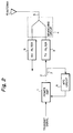
- FIG. 2 shows a specific conventional mobile communication device in which a coupler 7 intervenes between a power amplifier 1 and a TX filter 3, i.e., it does not follow the TX filter 3.
- a coupler 7 intervenes between a power amplifier 1 and a TX filter 3, i.e., it does not follow the TX filter 3.
- FIG. 2 there are also shown a branching circuit 4, an APC circuit 8, and a RX filter 9.
- the TX filter 13, branching circuit 14, RX filter 19, and coupler 17 included in the circuit 14 constitute the duplexer 20 which is a single unit or part. It follows that the number of parts of the device which need adjustment after assembly is reduced. Consequently, the output power control circuitry can be implemented easily in a small size.
- FIG. 3 an alternative embodiment of the present invention will be described.
- the same constituent parts as the parts shown in FIG. 1 are designated by the same reference numerals, and a detailed description thereof will not be made in order to avoid redundancy.
- this embodiment is similar to the previous embodiment except that the coupler 17 is inserted in the radio frequency signal line 15 connecting the branching circuit 14 and the antenna 16. However, the coupler 17 is again located to follow the TX filter 13. This embodiments operates in the same manner as the previous embodiment although the position of the coupler 17 is different.
- the embodiment described with reference to FIG. 3 has the following advantages.
- frequency deviation refers to an occurrence that the output power of the signal fed from the branching circuit 14 to the radio frequency path 15 changes with a change in the frequency of the signal. Another advantage is that the embodiment is practicable with a commercially available duplexer.
- the coupler 17 senses the levels of received signals more than in the previous embodiment.
- the detection voltage will be free from the influence of the received signal if the output power control loop is activated only during transmission, as stated in relation to the previous embodiment. Further, the detection voltage can be freed from the influence of the reflected signal if the sensitivity of the coupler 17 and that of the detector 30 are selected adequately.
- a mobile communication device having output power control circuitry has an output power sensor succeeding a TX filter and causes an output power control loop to operate in response to the output of the sensor.
- the device surely controls output power to a preselected value.
- a duplexer has the output power sensor in its branching circuit. This implements the output power control circuitry and, therefore, a mobile communication device incorporating with ease in a miniature configuration for the following reason. If the power output sensor is not included in the duplexer and located to follow the TX filter, the person designing the device must additionally take account of, for example, the coupling state between the filter and an antenna. This increases the range of parts and coupling which should be taken into account. Moreover, if the various parts of the duplexer are not arranged integrally with each other, the number of parts needing adjustment after assembly increases, and the adjustment is complicated. To facilitate the adjustment, the individual parts should be strictly controlled in performance.
Landscapes
- Engineering & Computer Science (AREA)
- Computer Networks & Wireless Communication (AREA)
- Signal Processing (AREA)
- Transmitters (AREA)
- Tone Control, Compression And Expansion, Limiting Amplitude (AREA)
- Control Of Amplification And Gain Control (AREA)
- Mobile Radio Communication Systems (AREA)
- Transceivers (AREA)
Abstract
Description
- The present invention relates to a mobile communication device, and output power control circuitry and duplexer applicable thereto.
- It is a common practice to provide a mobile communication device, e.g., mobile phone with output power control circuitry. The control circuitry selects one of several different output power levels matching the current distance between the mobile phone and a base station, while stabilizing the output power. We describe the conventional control circuitry. A power amplifier amplifies the power of a signal to be transmitted, i.e., a carrier modulated by a speech signal or similar signal. The amplified signal is delivered to a transmitter filter (TX filter) via a first radio frequency signal path. The TX filter limits the input signal to a predetermined frequency band for transmission. The output of the TX filter is routed through a branching circuit, which isolates a transmission section and a receipt section, and a second radio frequency signal path to an antenna. As a result, the signal to be transmitted is radiated from the antenna to the air as an electromagnetic wave.
- A coupler is inserted in the first radio frequency signal path. The coupler produces part of the output signal of the power amplifier from the above path. The produced signal (part of the power amplifier output) is fed from the coupler to an automatic power control (APC) circuit in the form of an electric signal. At the same time, a controller, controlling the entire mobile phone, feeds to the APC circuit a reference signal indicative of power to be output from the mobile phone and matching the current distance between the mobile phone and a base station. The APC circuit compares the produced signal and the reference signal and thereby generates a gain control signal for matching the former to the latter. The gain control signal from the APC circuit is applied to the power amplifier so as to stabilize the output power of the power amplifier at a predetermined value.
- Usually the TX filter and branching circuit are constructed into a single unit or part together with a receiver filter (RX filter) and are put on the market as a duplexer.
- The conventional output power control circuitry is capable of controlling the output signal of the power amplifier to a preselected size, as stated above. However, the conventional circuitry has the following problem left unsolved. The TX filter is located to follow the power amplifier and closer to the antenna than the amplifier. In this condition, the output power of the TX filter and, therefore, that of the antenna has a frequency characteristic which is not flat due to the influence of the pass band deviation and low return loss of the TX filter. The words "pass band deviation" should be understood, throughout the following description, to refer to the fact that the attenuation factor of the TX filter, implemented by a band-pass filter, varies with frequencies lying in the pass band of the filter. Because the frequency of the signal to be transmitted corresponds to a channel currently occupied for transmission, the above problem means that the output power differs from one channel to another channel for transmission.
- For example, a certain kind of mobile phone available today must match itself to a great number of transmission channels having a carrier frequency range of from 824 MHz to 849 MHz. The TX filter is, therefore, required to have a pass band as broad as 25 MHz. In addition, the TX filter should discriminate frequencies with high accuracy at the boundaries between its pass band and the outside of the same. Consequently, some degree of pass band deviation is not avoidable in the TX filter.
- To obviate the above drawback attributable to the non-flat frequency characteristic of the output power, it has been customary with a mobile phone to use a TX filter having a minimum of pass band deviation. Although this kind of approach reduces the drawback, it is not a drastic measure capable of eliminating it. In these circumstances, there is a demand for an implementation capable of controlling the output power to a preselected value stably despite the pass band deviation of the TX filter.
- It is, therefore, an object of the present invention to provide a mobile communication device capable of maintaining, despite the pass band deviation and low return loss of a TX filter, the output power of a signal to be transmitted constant without regard to the frequency of the signal.
- It is another object of the present invention to provide new and useful output power control circuitry and duplexer for implementing the above mobile communication device.
- In accordance with the present invention, a mobile communication device has a power amplifier for amplifying the power of a signal to be transmitted, a TX filter for limiting the frequency band of the signal amplified by the power amplifier to a predetermined frequency band for transmission, an antenna for radiating the signal limited in frequency band by the TX filter to the air, and output power control circuitry for controlling the output power of the signal to be transmitted. The output power control circuitry has an output power sensor succeeding the TX filter in the direction of flow of the signal to be transmitted, and for sensing the output power of the signal, and an automatic power control circuit for controlling the gain of the power amplifier such that the output power sensed by the output power sensor coincides with a predetermined reference value.
- Also, in accordance with the present invention, output power control circuitry for a mobile communication device which amplifies the power of a signal to be transmitted by a power amplifier, limits the frequency band of the signal amplified by the power amplifier to a predetermined frequency band for transmission by a TX filter, and transmits the signal lying in the predetermined frequency band via an antenna has an output power sensor succeeding the TX filter in the direction of flow of the signal to be transmitted, and for sensing the output power of the signal. An automatic power control circuit controls the gain of the power amplifier such that the output power sensed by the output power sensor coincides with a predetermined reference value.
- Further, in accordance with the present invention, a duplexer has a TX filter for limiting the frequency band of a signal to be fed to an antenna to a predetermined frequency band for transmission. A RX filter separates from a signal coming in through the antenna the frequency components lying in a predetermined frequency band for receiving. A branching circuit isolates the TX filter and the RX filter connected to the antenna. An output power sensor is provided on a transmission path included in the branching circuit, and senses the output power of the signal to be fed to the antenna.
- The objects and features of the present invention will become more apparent from the consideration of the following detailed description taken in conjunction with the accompanying drawings in which:
- FIG. 1 is a block diagram schematically showing a mobile communication device embodying the present invention;
- FIG. 2 is a block diagram schematically showing a conventional mobile communication device having a coupler preceding a TX filter;
- FIG. 3 is a block diagram schematically showing an alternative embodiment of the present invention;
- FIG. 4 is a plan view showing a specific configuration of a coupler included in the embodiments;
- FIG. 5 is a circuit diagram representative of a detector also included in the embodiments; and
- FIG. 6 is a circuit diagram showing a specific arrangement of a power amplifier further included in the embodiments.
- Referring to FIG. 1 of the drawings, a mobile communication device embodying the present invention is shown. As shown, the device has a
power amplifier 11 forming part of a transmission section and connected to aduplexer 20 by a first radiofrequency signal line 12. A radio frequency (RF)circuit 41 and an intermediate frequency (IF)circuit 42 form part of a receiving section. Anantenna 16 is connected to theduplexer 20 by a second radiofrequency signal line 15. An automatic power control (APC)circuit 18 controls the gain of thepower amplifier 11, as will be described specifically later. Acontroller 50 controls the various constituents of the device. For example, when thecontroller 50 receives a received signal strength indication (RSSI) from theIF circuit 42, it generates areference signal 51 for generating a reference voltage and feeds it to theAPC circuit 18. - The
duplexer 20 is made up of aTX filter 13, aRX filter 19, abranching circuit 14, and acoupler 17. Theseconstituents duplexer 20 are constructed into a single unit or part. Thebranching circuit 14 isolates the transmission section and the receiving section of the device from each other. Thecoupler 17 andAPC circuit 18 constitute output power control circuitry in combination. - In FIG. 1, there are not shown the parts of the device not relevant to the understanding of the present invention. These parts include a circuit for modulating a carrier with a speech signal to thereby generate a signal to be transmitted, a circuit for demodulating a received signal, a dialing section, a display for displaying a telephone number and other necessary information, a speaker, and a microphone.
- The signal to be transmitted is amplified by the
power amplifier 11 and then applied to theTX filter 13. TheTX filter 13 limits the input signal to a predetermined frequency band for transmission. The output of theTX filter 13 is routed through the branchingcircuit 14 and radiofrequency signal line 15 to theantenna 16 and radiated from theantenna 16 to the air as an electromagnetic wave. On the other hand, a signal coming in through theantenna 16 is applied to theRX filter 19 via the branchingcircuit 14. TheRX filter 19 separates only the signal components lying in a predetermined frequency band for receiving. The resulting output of theRX filter 19 is amplified by theRF circuit 41 and then transformed to a first intermediate frequency (first IF). TheIF circuit 42 receives the first IF from theRF circuit 41 and transforms it to a second intermediate frequency (second IF). At the same time, theIF circuit 42 delivers to thecontroller 50 the signal not transformed to the second IF as the previously mentioned RSSI. - The illustrative embodiment differs from the conventional device in respect of a control loop for controlling the output power. Specifically, the
coupler 17, playing the role of an output power sensor, is inserted in aradio frequency path 21 included in the branchingcircuit 14 and assigned to transmission. As shown in FIG. 4 specifically, thecoupler 17 has adielectric substrate 173 and twoconductors substrate 173. With such a microstrip line type configuration, thecoupler 17 serves as a side-coupling directional coupler. Thecoupler 17 produces part of the output signal of theTX filter 13 from theradio frequency path 21 and delivers it to theAPC circuit 18 in the form of an electric signal. Thereference signal 51 is applied from thecontroller 50 to theAPC circuit 18, as stated earlier. TheAPC circuit 18 generates, based on the output of thecoupler 17 andreference signal 51, a gain control signal for matching the power of the output of theTX filter 13 to thereference signal 51. The gain control signal is fed to thepower amplifier 11. - While the
coupler 17 is a specific form of an output power sensor and may be replaced with, for example, a branch line, it is more desirable than the others because it scarcely affects the transmission of a signal. In this embodiment, thecoupler 17 disposed in the branchingcircuit 17 forms part of theduplexer 20 together with theTX filter 13, branchingcircuit 14, andRX filter 19. - The
APC circuit 18 has adetector 30, acomparator 32, and areference voltage generator 33. Thedetector 30 detects the output of thecoupler 17 and generates a detection voltage (DC voltage) representative of its mean level. The detection signal from thedetector 30 is fed to thecomparator 31. Because thecoupler 17 is disposed in the branchingcircuit 14, it produces even part of the reflected signal from theradio frequency path 21. However, this part is far lower in level than the produced part of the signal to be transmitted. Therefore, the detection voltage can be freed from the influence of the reflected signal if the sensitivity of thecoupler 17 and that of thedetector 30 are selected adequately. - To change the detection sensitivity, in the specific configuration of FIG. 4, the distance between the two
lines dielectric substrate 173 may be changed to change the dielectric constant in the gap between thelines detector 30. As shown, thedetector 30 has adiode 301,capacitors resistors detector 30 performs half-wave rectification with a signal to be transmitted and undergone frequency modulation (FM), thereby separating a DC component. In this case, the detection sensitivity may be changed by varying the capacity of thecapacitor 302. Further, assume that the output of thedetector 30 is divided in voltage by two resistors, and the divided voltage is applied to theamplifier 32, FIG. 1. Then, the detection sensitivity may be changed by varying the ratio between the two resistors. It is to be noted that the detection sensitivity is selected at the design stage of the communication device. - When the communication device has an access system conforming to a TDD (Time Division Duplex) system or Ping-Pong transmission system, the detection voltage will be free from the influence of the received signal if an output power control loop, which will be described later, is activated only during transmission. Presumably, inserting the
coupler 17 in the branchingcircuit 14 has not been taken thought of in the past in fear of that it would produce even part of the reflected signal from theradio frequency path 21. - In the
APC circuit 18, areference voltage 52 from thereference voltage generator 33 is also applied to thecomparator 31. Specifically, thereference voltage 52 is generated by thecontroller 50 andreference voltage generator 33, as follows. Thecontroller 50 determines, in response to the output RSSI of theIF circuit 42 and representative of the strength of a received signal, the reference value of the output power of a signal to be sent. The reference value is any one of, for example, eight stepwise values which are different by each 4 dB. Thereference signal 51 from thecontroller 50 designates one of the eight different reference values, i.e., has one of values of "0" to "7" corresponding to the determined reference value. Thereference signal 51 is a three-bit signal and delivered to thereference voltage generator 33 over three signal lines. In response, thegenerator 33 generates areference voltage 52 corresponding to the designated reference value. - An alternative scheme replacing the RSSI scheme stated above is as follows. Assume that a command relating to the reference value of the output power is sent from a base station to the communication device as part of control data. Then, the
controller 50 will select an adequate reference value as designated by the command from the base station. - The
comparator 31 produces a voltage representative of a difference between the instantaneous detection voltage from thedetector 30 and thereference voltage 52 from thereference voltage generator 33, i.e., between the actual output power and the reference output power. The voltage from thecomparator 31 is amplified by theamplifier 32 and then fed to thepower amplifier 11 as again control signal 181. - When the
power amplifier 11 comprises an FET (Field-Effect Transistor) for amplifying the signal to be transmitted, thegain control signal 181 may be the voltage applied to the drain of the FET. In this case, in order to increase the gain of the FET, the drain voltage, i.e., the gain control signal is increased. FIG. 6 shows the power amplifier including twoFETs gain control signal 181 is applied to the drain electrode of preceding one of theFETs FETs power amplifier 11 comprises strip lines 121-123, stubs 124-127, capacitors 131-142, and resistors 151-156. A voltage VG1 and thegain control signal 181 are applied to, the gate electrode and the drain electrode of theFET 111, respectively. Voltages VG2 and VD are applied to the gate electrode and the drain electrode of theFET 112, respectively. - As a result, the gain of the
power amplifier 11 is so changed as to bring the detection voltage into coincidence with the reference voltage. This provides the output of theTX filter 13, i.e., the signal to be transmitted with the preselected power. Even if theTX filter 13 has a pass band deviation and low return loss, the output of thefilter 13 surely achieves the preselected power without regard to its frequency because the output power control loop operates on the basis of the deviation of the detection voltage, which is detected from the output of thefilter 13, from the reference voltage. - As stated above, in the illustrative embodiment, the coupler or
output power sensor 17 is inserted in theradio frequency path 21 included in the branchingcircuit 14 and assigned to transmission. Thecoupler 17 forms part of the output power control loop. Hence, even when theTX filter 13 has a pass band deviation and low return loss, the output power can be stably controlled to a preselected value. This successfully prevents the output power from differing from one channel (carrier frequency) to another channel. - FIG. 2 shows a specific conventional mobile communication device in which a
coupler 7 intervenes between a power amplifier 1 and aTX filter 3, i.e., it does not follow theTX filter 3. In this circuitry, it is likely that the output power changes from one channel to another channel because a signal to be transmitted via anantenna 6 is susceptible to the pass band deviation and low return loss of theTX filter 3. In FIG. 2, there are also shown a branching circuit 4, anAPC circuit 8, and aRX filter 9. - Further, in the above embodiment, the
TX filter 13, branchingcircuit 14,RX filter 19, andcoupler 17 included in thecircuit 14 constitute theduplexer 20 which is a single unit or part. It follows that the number of parts of the device which need adjustment after assembly is reduced. Consequently, the output power control circuitry can be implemented easily in a small size. - Referring to FIG. 3, an alternative embodiment of the present invention will be described. In FIG. 3, the same constituent parts as the parts shown in FIG. 1 are designated by the same reference numerals, and a detailed description thereof will not be made in order to avoid redundancy. As shown, this embodiment is similar to the previous embodiment except that the
coupler 17 is inserted in the radiofrequency signal line 15 connecting the branchingcircuit 14 and theantenna 16. However, thecoupler 17 is again located to follow theTX filter 13. This embodiments operates in the same manner as the previous embodiment although the position of thecoupler 17 is different. - The embodiment described with reference to FIG. 3 has the following advantages. First, even when the
TX filter 13 has a pass band deviation and low return loss, the output power can be stably controlled to a preselected value, as stated in relation to the previous embodiment. This successfully prevents the output power from differing from one channel (carrier frequency) to another channel. Assume that a frequency deviation and low return loss are caused by the mismatching between the branchingcircuit 14 and the radiofrequency signal path 15 connected to theantenna 16. Even in this condition, the output power can be stabilized at a preselected value because thecoupler 17 is inserted in thepath 15, and the control loop operates in response to the output of thecoupler 17. This also prevents the output power from differing from one channel (carrier frequency) to another channel. The words "frequency deviation" mentioned above refer to an occurrence that the output power of the signal fed from the branchingcircuit 14 to theradio frequency path 15 changes with a change in the frequency of the signal. Another advantage is that the embodiment is practicable with a commercially available duplexer. - In the alternative embodiment, the
coupler 17 senses the levels of received signals more than in the previous embodiment. However, when the device has an access system conforming to a TDD system or Ping-Pong transmission system, the detection voltage will be free from the influence of the received signal if the output power control loop is activated only during transmission, as stated in relation to the previous embodiment. Further, the detection voltage can be freed from the influence of the reflected signal if the sensitivity of thecoupler 17 and that of thedetector 30 are selected adequately. - In summary, in accordance with the present invention, a mobile communication device having output power control circuitry has an output power sensor succeeding a TX filter and causes an output power control loop to operate in response to the output of the sensor. Hence, even when the TX filter involves a pass band deviation and low return loss, the device surely controls output power to a preselected value.
- Also, in accordance with the present invention, a duplexer has the output power sensor in its branching circuit. This implements the output power control circuitry and, therefore, a mobile communication device incorporating with ease in a miniature configuration for the following reason. If the power output sensor is not included in the duplexer and located to follow the TX filter, the person designing the device must additionally take account of, for example, the coupling state between the filter and an antenna. This increases the range of parts and coupling which should be taken into account. Moreover, if the various parts of the duplexer are not arranged integrally with each other, the number of parts needing adjustment after assembly increases, and the adjustment is complicated. To facilitate the adjustment, the individual parts should be strictly controlled in performance.
- While the present invention has been described with reference to the particular illustrative embodiments, it is not to be restricted by the embodiments. It is to be appreciated that those skilled in the art can change or modify the embodiments without departing from the scope and spirit of the present invention. For example, while the embodiments have concentrated on a mobile phone, the present invention is, of course, applicable to a transceiver or similar mobile communication device. Further, the present invention is applicable even to a transmitting device and or a base station included in a mobile communication system.
Claims (10)
- A mobile communication device having a power amplifier (11) for amplifying power of a signal to be transmitted, a transmitter filter (13) for limiting a frequency band of the signal amplified by said power amplifier (11) to a predetermined frequency band for transmission, an antenna (16) for radiating the signal limited in frequency band by said transmitter filter (13) to the air, and output power control circuitry for controlling output power of the signal to be transmitted;
CHARACTERIZED IN THAT
said output power control circuitry comprises:
an output power sensor (17) succeeding said transmitter filter (13) in a direction of flow of the signal to be transmitted, and for sensing the output power of said signal; and
an automatic power control circuit (18) for controlling a gain of said power amplifier (11) such that the output power sensed by said output power sensor (17) coincides with a predetermined reference value. - A device in accordance with claim 1, CHARACTERIZED IN THAT said device and said antenna (16) each has a transmitting function and a receiving function, said device further comprises a branching circuit (14) isolating a transmitting section and a receiving section connected to said antenna (16), and said output power sensor (17) is provided on a transmission path (21) included in said branching circuit (14).
- A device in accordance with claim 1, CHARACTERIZED IN THAT said device and said antenna (16) each has a transmitting function and a receiving function, said device further comprises a branching circuit isolating a transmitting section and a receiving section connected to said antenna (16), and said output power sensor (17) is provided on a path (15) connecting said branching circuit (14) and said antenna (16).
- A device in accordance with claim 1, CHARACTERIZED IN THAT said output power sensor (17) comprises a coupler.
- Output power control circuitry for a mobile communication device which amplifies power of a signal to be transmitted by a power amplifier (11), limits a frequency band of the signal amplified by said power amplifier (11) to a predetermined frequency band for transmission by a transmitter filter (13), and transmits the signal lying in said predetermined frequency band via an antenna (16);
CHARACTERIZED IN THAT
an output power sensor (17) succeeds said transmitter filter (13) in the direction of flow of the signal to be transmitted, and senses the output power of the signal; and
an automatic power control circuit (18) controls a gain of said power amplifier (11) such that the output power sensed by said output power sensor (17) coincides with a predetermined reference value. - Circuitry in accordance with claim 5, CHARACTERIZED IN THAT said device and said antenna (16) each has a transmitting function and a receiving function, said device further comprises a branching circuit (14) isolating a transmitting section and a receiving section connected to said antenna (16), and said output power sensor (17) is provided on a transmission path (21) included in said branching circuit.
- Circuitry in accordance with claim 5, CHARACTERIZED IN THAT said device and said antenna (16) each has a transmitting function and a receiving function, said device further comprises a branching circuit (14) isolating a transmitting section and a receiving section connected to said antenna (16), and said output power sensor (17) is provided on a path (15) connecting said branching circuit (14) and said antenna (16).
- Circuitry in accordance with claim 5, CHARACTERIZED IN THAT said output power sensor (17) comprises a coupler.
- An antenna duplexer (20) comprising a transmitter filter (13) for limiting a frequency band of a signal to be fed to an antenna to a predetermined frequency band for transmission, a receiver filter (19) for separating from a signal coming in through the antenna frequency components lying in a predetermined frequency band for receiving, and a branching circuit (14) for isolating said transmitter filter (13) and said receiver filter (19) connected to said antenna (16);
CHARACTERIZED IN THAT
an output power sensor (17) is provided on a transmission path (21) included in said branching circuit (14), and senses an output power of the signal to be fed to said antenna (16). - A duplexer in accordance with claim 9, CHARACTERIZED IN THAT said output power sensor (17) comprises a coupler.
Applications Claiming Priority (3)
| Application Number | Priority Date | Filing Date | Title |
|---|---|---|---|
| JP17231794A JPH0837434A (en) | 1994-07-25 | 1994-07-25 | Output power control circuit and antenna multicoupler for mobile communication equipment |
| JP17231794 | 1994-07-25 | ||
| JP172317/94 | 1994-07-25 |
Publications (3)
| Publication Number | Publication Date |
|---|---|
| EP0695031A2 true EP0695031A2 (en) | 1996-01-31 |
| EP0695031A3 EP0695031A3 (en) | 1997-11-05 |
| EP0695031B1 EP0695031B1 (en) | 2002-10-23 |
Family
ID=15939678
Family Applications (1)
| Application Number | Title | Priority Date | Filing Date |
|---|---|---|---|
| EP95111525A Expired - Lifetime EP0695031B1 (en) | 1994-07-25 | 1995-07-21 | Mobile communication device having an output power sensor succeeding a transmission filter |
Country Status (7)
| Country | Link |
|---|---|
| US (1) | US5715527A (en) |
| EP (1) | EP0695031B1 (en) |
| JP (1) | JPH0837434A (en) |
| KR (1) | KR100297618B1 (en) |
| CN (1) | CN1066307C (en) |
| CA (1) | CA2154530A1 (en) |
| DE (1) | DE69528616T2 (en) |
Cited By (5)
| Publication number | Priority date | Publication date | Assignee | Title |
|---|---|---|---|---|
| WO2000075905A1 (en) * | 1999-06-07 | 2000-12-14 | Johnson Controls Technology Company | Transceiver with closed loop control of antenna tuning and power level |
| US6334050B1 (en) | 1997-06-13 | 2001-12-25 | Telefonaktiebolaget Lm Ericsson (Publ) | Arrangement and a method relating to a radio unit |
| EP1142136A4 (en) * | 1998-12-31 | 2002-05-08 | Nokia Corp | GAIN CONTROL AND POWER CONSUMPTION IN A POWER AMPLIFIER |
| EP1313227A4 (en) * | 2000-08-22 | 2009-07-22 | Hitachi Metals Ltd | Laminated high-frequency switch module |
| CN102916708A (en) * | 2012-10-19 | 2013-02-06 | 北京中科飞鸿科技有限公司 | Power adjustment device of radio emitter and radio emitter |
Families Citing this family (31)
| Publication number | Priority date | Publication date | Assignee | Title |
|---|---|---|---|---|
| JP3124229B2 (en) * | 1996-06-28 | 2001-01-15 | 富士通株式会社 | Wireless base station in WLL system using PHS, operation method thereof, and interface converter |
| US6018650A (en) * | 1996-12-18 | 2000-01-25 | Aironet Wireless Communications, Inc. | Cellular communication devices with automated power level adjust |
| JPH10190381A (en) * | 1996-12-27 | 1998-07-21 | Fujitsu Ltd | Transceiver |
| CA2264125C (en) | 1998-03-03 | 2003-05-06 | Nec Corporation | Method of controlling transmission power in a cellular type mobile communication system |
| FI990687L (en) * | 1999-03-29 | 2000-09-30 | Nokia Mobile Phones Ltd | Wireless communication antenna matching system |
| US6779146B1 (en) | 1999-04-05 | 2004-08-17 | Cisco Technology, Inc. | ARQ for point to point links |
| FR2813487B1 (en) * | 2000-08-31 | 2002-11-29 | Cit Alcatel | METHOD AND DEVICE FOR CONTROLLING THE AMPLIFICATION OF THE SIGNAL TRANSMITTED BY A MOBILE TERMINAL FOR INCREASING THE AUTONOMY OF SAID MOBILE TERMINAL |
| US20030054780A1 (en) * | 2000-09-05 | 2003-03-20 | Hitachi, Ltd. | High frequency power amplifying circuit, and mobile communication apparatus using it |
| KR100377928B1 (en) | 2001-05-11 | 2003-03-29 | 삼성전자주식회사 | Signal interference cancellation method and apparatus of local wireless communication apparatus mounted on mobile terminal |
| US6701138B2 (en) * | 2001-06-11 | 2004-03-02 | Rf Micro Devices, Inc. | Power amplifier control |
| US6724252B2 (en) * | 2002-02-21 | 2004-04-20 | Rf Micro Devices, Inc. | Switched gain amplifier circuit |
| GB0212740D0 (en) * | 2002-05-31 | 2002-07-10 | Hitachi Ltd | Transmitter and wireless communication apparatus using the transmitter |
| US20040072549A1 (en) * | 2002-10-10 | 2004-04-15 | Sanford John Richard | Communication device with front-end antenna and filter integration |
| US20040072551A1 (en) * | 2002-10-10 | 2004-04-15 | Sanford John Richard | Communication device with front-end integration |
| US20040072542A1 (en) * | 2002-10-10 | 2004-04-15 | Sanford John Richard | Communication device with integration in separate transmitter and receiver antennas |
| US20040070454A1 (en) * | 2002-10-15 | 2004-04-15 | Triquint Semiconductor, Inc. | Continuous bias circuit and method for an amplifier |
| US6701134B1 (en) | 2002-11-05 | 2004-03-02 | Rf Micro Devices, Inc. | Increased dynamic range for power amplifiers used with polar modulation |
| US7177370B2 (en) * | 2003-12-17 | 2007-02-13 | Triquint Semiconductor, Inc. | Method and architecture for dual-mode linear and saturated power amplifier operation |
| US7109791B1 (en) | 2004-07-09 | 2006-09-19 | Rf Micro Devices, Inc. | Tailored collector voltage to minimize variation in AM to PM distortion in a power amplifier |
| US7336127B2 (en) * | 2005-06-10 | 2008-02-26 | Rf Micro Devices, Inc. | Doherty amplifier configuration for a collector controlled power amplifier |
| US7330071B1 (en) | 2005-10-19 | 2008-02-12 | Rf Micro Devices, Inc. | High efficiency radio frequency power amplifier having an extended dynamic range |
| CN100388825C (en) * | 2005-10-24 | 2008-05-14 | 华为技术有限公司 | A signal combination device and base station common antenna feeder system realized by using it |
| US7970427B2 (en) * | 2007-03-20 | 2011-06-28 | Skyworks Solutions, Inc. | System and method for dynamically improving call connection |
| JP4642133B2 (en) * | 2007-08-02 | 2011-03-02 | 富士通株式会社 | Wireless transceiver |
| US20090137217A1 (en) * | 2007-11-27 | 2009-05-28 | Huang Chung-Er | Communication transmission system and power detection method thereof |
| US8731492B2 (en) | 2008-07-17 | 2014-05-20 | Freescale Semiconductor, Inc. | System for monitoring and controlling the power of a radio frequency (RF) signal in a short-range RF transmitter |
| US9226299B1 (en) * | 2014-09-16 | 2015-12-29 | Sprint Spectrum L.P. | Dynamic frequency assignment based on both the distance from eNodeB and the loss of a band-pass filter |
| CN105262451A (en) * | 2015-10-27 | 2016-01-20 | 广州海格通信集团股份有限公司 | Fast automatic power closed-loop control device and method of wireless power amplifier |
| CN107565989B (en) * | 2017-09-28 | 2020-07-10 | 歌尔股份有限公司 | Unmanned aerial vehicle broadband antenna multiplexing method and device |
| US11038474B2 (en) | 2017-11-01 | 2021-06-15 | Analog Devices Global Unlimited Company | Phased array amplifier linearization |
| KR102512781B1 (en) * | 2020-06-30 | 2023-03-22 | 주식회사 아모센스 | System for testing a performance of antenna |
Family Cites Families (5)
| Publication number | Priority date | Publication date | Assignee | Title |
|---|---|---|---|---|
| US4523155A (en) * | 1983-05-04 | 1985-06-11 | Motorola, Inc. | Temperature compensated automatic output control circuitry for RF signal power amplifiers with wide dynamic range |
| US4792939A (en) * | 1986-01-24 | 1988-12-20 | Hitachi Denshi Kabushiki Kaisha | Duplex radio communication transceiver |
| JPH0425220A (en) * | 1990-05-21 | 1992-01-29 | Toshiba Corp | Automatic power control circuit |
| US5212815A (en) * | 1991-09-03 | 1993-05-18 | Motorola, Inc. | Radio equipment directional coupler |
| SE513813C2 (en) * | 1993-02-05 | 2000-11-06 | Ericsson Ge Mobile Communicat | Device with SAW filter for duplex transmission |
-
1994
- 1994-07-25 JP JP17231794A patent/JPH0837434A/en active Pending
-
1995
- 1995-05-24 KR KR1019950013044A patent/KR100297618B1/en not_active Expired - Fee Related
- 1995-07-21 CN CN95108930A patent/CN1066307C/en not_active Expired - Fee Related
- 1995-07-21 EP EP95111525A patent/EP0695031B1/en not_active Expired - Lifetime
- 1995-07-21 DE DE69528616T patent/DE69528616T2/en not_active Expired - Fee Related
- 1995-07-24 US US08/506,123 patent/US5715527A/en not_active Expired - Lifetime
- 1995-07-24 CA CA002154530A patent/CA2154530A1/en not_active Abandoned
Non-Patent Citations (1)
| Title |
|---|
| None |
Cited By (5)
| Publication number | Priority date | Publication date | Assignee | Title |
|---|---|---|---|---|
| US6334050B1 (en) | 1997-06-13 | 2001-12-25 | Telefonaktiebolaget Lm Ericsson (Publ) | Arrangement and a method relating to a radio unit |
| EP1142136A4 (en) * | 1998-12-31 | 2002-05-08 | Nokia Corp | GAIN CONTROL AND POWER CONSUMPTION IN A POWER AMPLIFIER |
| WO2000075905A1 (en) * | 1999-06-07 | 2000-12-14 | Johnson Controls Technology Company | Transceiver with closed loop control of antenna tuning and power level |
| EP1313227A4 (en) * | 2000-08-22 | 2009-07-22 | Hitachi Metals Ltd | Laminated high-frequency switch module |
| CN102916708A (en) * | 2012-10-19 | 2013-02-06 | 北京中科飞鸿科技有限公司 | Power adjustment device of radio emitter and radio emitter |
Also Published As
| Publication number | Publication date |
|---|---|
| CN1066307C (en) | 2001-05-23 |
| DE69528616D1 (en) | 2002-11-28 |
| EP0695031A3 (en) | 1997-11-05 |
| KR100297618B1 (en) | 2001-10-24 |
| EP0695031B1 (en) | 2002-10-23 |
| CA2154530A1 (en) | 1996-01-26 |
| KR960006357A (en) | 1996-02-23 |
| DE69528616T2 (en) | 2003-06-12 |
| US5715527A (en) | 1998-02-03 |
| CN1120784A (en) | 1996-04-17 |
| JPH0837434A (en) | 1996-02-06 |
Similar Documents
| Publication | Publication Date | Title |
|---|---|---|
| US5715527A (en) | Mobile communication device having an output power sensor succeeding a transmission filter | |
| US5363071A (en) | Apparatus and method for varying the coupling of a radio frequency signal | |
| EP0803973B1 (en) | Linear power amplifier with automatic gate/base bias control for optimum efficiency | |
| US5392464A (en) | Directional detector for power level control | |
| US5038112A (en) | Levelling control circuit | |
| US6233438B1 (en) | Wide-range power control systems and methods for radio frequency transmitters and mobile radiotelephones | |
| US4392245A (en) | Radio transmitter having an output power control circuit | |
| EP0241265B1 (en) | Radio transceiver including and antenna switching circuit capable of changing reception sensitivity | |
| US5150075A (en) | Power amplifier ramp up method and apparatus | |
| US5457814A (en) | Power boost system for cellular telephone | |
| EP0746118B1 (en) | Antenna switching circuit and wireless communication system | |
| EP0534681B1 (en) | Power booster for a radiotelephone | |
| US20060058072A1 (en) | Gain selected cell phone booster system | |
| US4367443A (en) | Radio frequency signal power amplifier | |
| EP0654898B1 (en) | Transmission circuit | |
| US5913154A (en) | VSWR control technique for terminal products with linear modulation | |
| JP2000295055A (en) | Transmitter and receiver | |
| US20040012441A1 (en) | RF power amplifier digital gain flattening over multiband frequencies | |
| US6549068B1 (en) | System and method for operating an RF power amplifier | |
| JP3623731B2 (en) | Mobile radio terminal device | |
| EP0359477A2 (en) | Linearization of an amplification in an RF amplifier | |
| JP3332408B2 (en) | Automatic power control circuit | |
| CN215498959U (en) | Antenna module for adjusting radio frequency load impedance in real time and mobile terminal | |
| US20060058071A1 (en) | Gain selected cell phone booster | |
| JPH1188082A (en) | Amplifying device and mobile phone device |
Legal Events
| Date | Code | Title | Description |
|---|---|---|---|
| PUAI | Public reference made under article 153(3) epc to a published international application that has entered the european phase |
Free format text: ORIGINAL CODE: 0009012 |
|
| AK | Designated contracting states |
Kind code of ref document: A2 Designated state(s): DE FR GB |
|
| PUAL | Search report despatched |
Free format text: ORIGINAL CODE: 0009013 |
|
| AK | Designated contracting states |
Kind code of ref document: A3 Designated state(s): DE FR GB |
|
| RIN1 | Information on inventor provided before grant (corrected) |
Inventor name: KOMAZAKI, TOMOKAZU C/O OKI ELECTRIC IND. CO., LTD Inventor name: GUNJI, KATSUHIKO C/O OKI ELECTRIC IND. CO., LTD. Inventor name: NAKANO, AKIRA C/O OKI ELECTRIC IND. CO., LTD. Inventor name: YASUOKA, TOSHIKAZU C/O OKI ELECTRIC IND. CO., LTD Inventor name: SHIMIZU, KOICHIRO C/O OKI ELECTRIC IND. CO., LTD. Inventor name: MIYAZAWA, TSUYOSHI C/O OKI ELECTRIC IND. CO., LTD Inventor name: IWATA, MASAO, C/O OKI ELECTRIC INDS. CO., LTD. Inventor name: HORII, HIROYUKI, C/O OKI ELECTRIC INDS. CO., LTD. |
|
| K1C3 | Correction of patent application (complete document) published |
Effective date: 19960131 |
|
| 17P | Request for examination filed |
Effective date: 19980407 |
|
| 17Q | First examination report despatched |
Effective date: 20000411 |
|
| GRAG | Despatch of communication of intention to grant |
Free format text: ORIGINAL CODE: EPIDOS AGRA |
|
| GRAG | Despatch of communication of intention to grant |
Free format text: ORIGINAL CODE: EPIDOS AGRA |
|
| GRAH | Despatch of communication of intention to grant a patent |
Free format text: ORIGINAL CODE: EPIDOS IGRA |
|
| GRAH | Despatch of communication of intention to grant a patent |
Free format text: ORIGINAL CODE: EPIDOS IGRA |
|
| GRAA | (expected) grant |
Free format text: ORIGINAL CODE: 0009210 |
|
| AK | Designated contracting states |
Kind code of ref document: B1 Designated state(s): DE FR GB |
|
| REG | Reference to a national code |
Ref country code: GB Ref legal event code: FG4D |
|
| REF | Corresponds to: |
Ref document number: 69528616 Country of ref document: DE Date of ref document: 20021128 |
|
| ET | Fr: translation filed | ||
| PLBE | No opposition filed within time limit |
Free format text: ORIGINAL CODE: 0009261 |
|
| STAA | Information on the status of an ep patent application or granted ep patent |
Free format text: STATUS: NO OPPOSITION FILED WITHIN TIME LIMIT |
|
| 26N | No opposition filed |
Effective date: 20030724 |
|
| PGFP | Annual fee paid to national office [announced via postgrant information from national office to epo] |
Ref country code: FR Payment date: 20090710 Year of fee payment: 15 |
|
| PGFP | Annual fee paid to national office [announced via postgrant information from national office to epo] |
Ref country code: GB Payment date: 20090715 Year of fee payment: 15 Ref country code: DE Payment date: 20090716 Year of fee payment: 15 |
|
| GBPC | Gb: european patent ceased through non-payment of renewal fee |
Effective date: 20100721 |
|
| REG | Reference to a national code |
Ref country code: FR Ref legal event code: ST Effective date: 20110331 |
|
| PG25 | Lapsed in a contracting state [announced via postgrant information from national office to epo] |
Ref country code: DE Free format text: LAPSE BECAUSE OF NON-PAYMENT OF DUE FEES Effective date: 20110201 |
|
| REG | Reference to a national code |
Ref country code: DE Ref legal event code: R119 Ref document number: 69528616 Country of ref document: DE Effective date: 20110201 |
|
| PG25 | Lapsed in a contracting state [announced via postgrant information from national office to epo] |
Ref country code: FR Free format text: LAPSE BECAUSE OF NON-PAYMENT OF DUE FEES Effective date: 20100802 |
|
| PG25 | Lapsed in a contracting state [announced via postgrant information from national office to epo] |
Ref country code: GB Free format text: LAPSE BECAUSE OF NON-PAYMENT OF DUE FEES Effective date: 20100721 |