EP0695016B1 - Current control interface circuit - Google Patents
Current control interface circuit Download PDFInfo
- Publication number
- EP0695016B1 EP0695016B1 EP19940202223 EP94202223A EP0695016B1 EP 0695016 B1 EP0695016 B1 EP 0695016B1 EP 19940202223 EP19940202223 EP 19940202223 EP 94202223 A EP94202223 A EP 94202223A EP 0695016 B1 EP0695016 B1 EP 0695016B1
- Authority
- EP
- European Patent Office
- Prior art keywords
- voltage
- circuit
- supply
- current control
- control interface
- Prior art date
- Legal status (The legal status is an assumption and is not a legal conclusion. Google has not performed a legal analysis and makes no representation as to the accuracy of the status listed.)
- Expired - Lifetime
Links
- 238000007599 discharging Methods 0.000 claims description 19
- 238000001514 detection method Methods 0.000 claims description 18
- 230000003213 activating effect Effects 0.000 claims description 9
- 239000003990 capacitor Substances 0.000 description 29
- 230000007423 decrease Effects 0.000 description 8
- 230000008878 coupling Effects 0.000 description 1
- 238000010168 coupling process Methods 0.000 description 1
- 238000005859 coupling reaction Methods 0.000 description 1
- 230000003247 decreasing effect Effects 0.000 description 1
Images
Classifications
-
- G—PHYSICS
- G05—CONTROLLING; REGULATING
- G05F—SYSTEMS FOR REGULATING ELECTRIC OR MAGNETIC VARIABLES
- G05F1/00—Automatic systems in which deviations of an electric quantity from one or more predetermined values are detected at the output of the system and fed back to a device within the system to restore the detected quantity to its predetermined value or values, i.e. retroactive systems
- G05F1/10—Regulating voltage or current
- G05F1/46—Regulating voltage or current wherein the variable actually regulated by the final control device is dc
- G05F1/468—Regulating voltage or current wherein the variable actually regulated by the final control device is dc characterised by reference voltage circuitry, e.g. soft start, remote shutdown
-
- G—PHYSICS
- G06—COMPUTING; CALCULATING OR COUNTING
- G06F—ELECTRIC DIGITAL DATA PROCESSING
- G06F13/00—Interconnection of, or transfer of information or other signals between, memories, input/output devices or central processing units
- G06F13/38—Information transfer, e.g. on bus
- G06F13/40—Bus structure
- G06F13/4063—Device-to-bus coupling
- G06F13/4068—Electrical coupling
-
- H—ELECTRICITY
- H02—GENERATION; CONVERSION OR DISTRIBUTION OF ELECTRIC POWER
- H02H—EMERGENCY PROTECTIVE CIRCUIT ARRANGEMENTS
- H02H9/00—Emergency protective circuit arrangements for limiting excess current or voltage without disconnection
- H02H9/001—Emergency protective circuit arrangements for limiting excess current or voltage without disconnection limiting speed of change of electric quantities, e.g. soft switching on or off
Definitions
- the present invention relates to a current control interface circuit interfacing between a power supply source and a load impedance which are able to be coupled across first and second supply terminals and first and second load terminals of said current control interface circuit, respectively, said second supply and load terminals being interconnected and said current control interface circuit including a variable impedance device which is coupled between said first supply and load terminals and has a control terminal coupled to said interconnected second supply and load terminals via a capacitance included in a capacitance charging and discharging circuit of which a charging part is operated upon an activating voltage being applied thereto, said charging and discharging circuit having a discharging part which includes a controlled discharge impedance device shunting said capacitance, said current control interface circuit further including a voltage detection circuit which is coupled between said first supply terminal and a control terminal of said discharge impedance device which is operated by a control voltage upon said voltage detection circuit detecting that a voltage at said first supply terminal is lower than a threshold voltage.
- variable impedance device is an n-channel mosfet of which the source and the drain are coupled to the first supply and first load terminals, respectively.
- the first load and supply terminals are carrying a voltage which is more negative than the one delivered by the interconnected second supply and load terminals. This seems to be in contrast to the situation which forms the object of the present invention, where the first supply and load terminals are at an electrical potential which is more positive with respect to the electrical potential delivered by the interconnected second supply and load terminals.
- the capacitor included in the charging and discharging circuit of the current control interface circuit, and intended to gradually turn on the variable impedance device is coupled between the control terminal of this variable impedance device and the interconnected second supply and load terminals which are at the most negative potential.
- the capacitor gradually turning on the variable impedance device is to be coupled in between the control terminal of this variable impedance device and its source terminal.
- the capacitance charging and discharging circuit of which the capacitor forms part further includes a current source in series with the capacitor, and consisting of prior art transistor F4 and prior art resistor R4 as can be observed from the figure of this prior art document.
- the discharging part of the capacitance charging and discharging circuit includes prior art transistor F2 constituting the controlled discharge impedance device which is shunting the capacitance.
- the charging part of the charging and discharging circuit is operated upon an activating voltage which is provided by coupling the second supply voltage terminal to the current source.
- This prior art current control interface circuit is coupled between a dc power supply and a dc-dc converter. Its function is to intercept fast and frequently occurring failures of the power supply so as to prevent the dc-dc converter from malfunctioning during these power supply failures.
- An additional capacitor is shunting the dc-dc converter, this parallel circuit thereby corresponding to the load impedance as described in the non-characteristic part of the first claim of the present invention, the load impedance thereby being equivalent with the parallel connection of a load resistor and a load capacitor.
- the capacitance of the prior art current control interface circuit is gradually charged by the current source operated upon switching on the power supply delivering the activating voltage.
- the mosfet constituting the variable impedance device thereby gradually turns on and the value of the drain-to-source path impedance changes from high ohmic to low ohmic.
- the load capacitor is charged by the power supply source without a peak in the total load current through the load impedance. Indeed, the value of the drain-to-source path resistance of the variable impedance device controls the total load current.
- the load current is delivered by the power supply source supplying the system voltage across the first and second supply terminals. A peak in load current could cause a peak in voltage across an internal resistance of the power supply source delivering the current, thereby causing the system voltage supplied by the power supply source to drop under the minimum voltage needed for the system to function properly.
- the prior art current control interface circuit further includes circuitry composed of a threshold circuit, denoted 3 in the figure of this prior art document, an output of which is coupled to a voltage divider composed of prior art resistors R2 and R6. An intersection point of this voltage divider is coupled to the input of an inverter composed of prior art transistor F3, and prior art resistors R5 and R9.
- This prior art threshold circuit together with the prior art voltage divider and the prior art inverter, thereby is to be considered as equivalent to the voltage detection circuit described in pre-characterising portion of the claim 1 of the present invention.
- the voltage detection circuit operates the controlled discharge impedance device to turn on, thereby discharging the capacitance, i.e. by shunting the capacitance with a low resistance.
- the capacitance is discharged whereby the variable impedance device is brought in its high ohmic impedance condition.
- the variable impedance device is off and has a high ohmic drain-to-source path resistance when the supply voltage is raised again. Due to the high ohmic drain-to-source path resistance a peak in the total load current is avoided.
- the first supply terminal of the current control interface circuit of the present invention is carrying the most positive potential.
- the prior art voltage detection circuit is detecting a voltage drop at the second supply terminal, which by means of equivalence corresponds to a voltage detection circuit which is adapted to detect voltage drops at the first supply terminal of the current control interface circuit of the present invention.
- the current control interface circuit is used in an application board, to be plugged in a so called system board including system circuits as well as the power supply source which continuously supplies the system voltage across the first and second supply terminals.
- the load impedance is permanently coupled to the current control interface circuit across the first and second load terminals.
- the voltage between both supply terminals does not drop immediately after pulling out of the application board, and therefore the voltage detection circuit does not immediately provide the appropriate control voltage to turn on the controlled discharge impedance device. Indeed, at the moment when the power supply source is disconnected from the supply terminals, the mosfet constituting the variable impedance device is still on. Therefore the voltage between the supply voltage terminals only gradually decreases via discharging of the load capacitance through the load resistance. As a consequence the voltage detection circuit does not deliver the appropriate output for turning on the controlled discharge device.
- the controlled discharge impedance device is able to quickly discharge the capacitance and as a result to quickly turn off the variable impedance device, its operation entirely depends on the detection, by the voltage detection circuit, of a voltage drop at the first supply terminal in the situation of the present invention. If this voltage is not sufficiently quickly dropping, the capacitance only discharges slowly. If the application board is afterwards plugged in again, the load capacitor has already been discharged but the capacitance may still be sufficiently charged for the mosfet constituting the variable impedance device to be on and thus have a low ohmic drain to source path resistance. The power supply source is thereby coupled to the uncharged load capacitor via the low impedance mosfet.
- An object of the present invention is thus to provide a current control interface circuit of the above known type but wherein the above mentioned problem of a too slow discharge of the capacitance during pulling out of the board, is solved.
- variable impedance device is coupled to said first supply terminal via an inductor device.
- the voltage at the first supply terminal drops immediately after the system voltage source is uncoupled from the first and second supply terminals. Indeed, the current through the inductor acting as a current source, decreases and thus the voltage across the latter device becomes negative and the voltage at the first supply terminal drops almost immediately.
- said voltage detection circuit includes an inverter circuit and a comparator circuit which compares said voltage at said first supply terminal with said threshold voltage, said inverter circuit inverting an output of said comparator circuit and supplying said control voltage to said control input of said discharge impedance device.
- the comparator output is active high (inactive low) when the voltage at the first supply terminal is above (below) a threshold. Due to the inverter circuit the output of the voltage detection circuit is then active low (inactive high) when the voltage at the first supply terminal is above (below) the predetermined threshold.
- An improvement of the present invention is the fact that said current control interface circuit includes a DC/DC converter circuit which is coupled to said first supply terminal and provides said activating voltage at its output which is coupled to said capacitance via a first resistance and to said inverter circuit.
- the inverter is still provided with the voltage across the charged capacitance via the first resistance when the system voltage source is uncoupled from the first and second supply terminals and when the DC/DC converter circuit does not provide the activating voltage at its output.
- said controlled discharge impedance device is constituted by an emitter to collector path of a first transistor of which a base is connected to said output of said inverter circuit which includes the series connection of a second resistance which is connected to said inverter output and of a second transistor of which a collector-to-emitter path shunts the base to emitter junction of said first transistor.
- the inverter and the discharge impedance both include a fast switching component, i.e. the first and second transistor, in order to limit the delay between the detection of the voltage drop at the first supply terminal and the discharging of the capacitance.
- variable impedance device is a FET of which a gate is said control terminal and of which a drain-to-source path is coupled between said first supply and load terminals.
- the capacitance does not discharge via the control terminal of the variable impedance device.
- the gate input resistance of a FET is high ohmic.
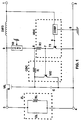
- the current control interface circuit includes supply terminals 1 and 2 and load terminals 3 and 4.
- Terminals 1 and 3 are interconnected via the series connection of an inductor DIFD and the drain-to-source path of a mosfet VIL.
- Terminals 2 and 4 are connected to a common ground reference.
- a load impedance ZL constituted by the parallel connection of a load capacitor CL and a load resistor RL is coupled across the load terminals 3 and 4.
- a gate of VIL is connected to the common ground reference via a control capacitor C which is shunted by a charging and discharging circuit CDC.
- CDC includes a discharge transistor VIC shunting capacitor C with a collector-to-emitter path and CDC further includes a charge resistor R connecting the collector of VIC to the output terminal of a DC/DC convertor circuit CONV which is connected to the common ground reference via a ground terminal 10 and of which an input terminal 9 is connected to the interconnection point between VIL and DIFD.
- the output terminal 8 of CONV is further connected to the common ground reference via the series connection of a resistor R1 and a collector-to-emitter path of a NPN transistor T1, R1 and T1 constituting an invertor circuit of which the output terminal 7 and input terminal 6 are the collector and a base of T1 respectively.
- the input terminal 6 of the invertor circuit i.e.
- the base of T1 is connected to an output terminal of a comparator circuit COMP of which an input terminal is connected to the supply terminal 1.
- the COMP circuit further has a ground terminal 5 connected to the common ground reference.
- the cascade connection of the COMP circuit and the above invertor circuit constitutes a voltage detection circuit VDC which is connected to the common ground reference and has an input terminal connected to the supply terminal 1, an output terminal 7 and an auxiliary voltage supply terminal connected to the output terminal 8 of the CONV circuit.
- the DC/DC converter CONV includes an integrated circuit MAXIM662, manufactured by Analog Devices and currently available on the market. In data sheets of the MAXIM662, the DC/DC converter is presented as a typical operating circuit using the latter integrated circuit. CONV is adapted to convert a voltage between 4,75 Volt and 5,5 Volt to a voltage of 12 Volt. It is to be noted that the output terminal of CONV is connected via an internal resistance path (not shown) to the common ground reference.
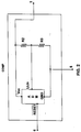
- the comparator circuit COMP depicted in Fig 2 includes an integrated circuit MAXIM697 hereafter referred to as ADM, manufactured by Analog Devices and currently available on the market.
- ADM has a power supply input Vcc, a voltage sensing input LLin, a ground terminal GND and an output RESET .
- the input terminal of COMP is connected to a power supply input Vcc of ADM and is further connected to the common ground reference via the series connection of resistors R2 and R3 constituting a voltage divider.
- the interconnection point of the latter resistors is connected to the voltage sensing input LLin of ADM.
- the ground terminal GND of ADM is connected to the common ground reference via the ground terminal 5 and the output RESET of ADM is the output terminal of COMP.
- control capacitor C when being charged up later, can not discharge via the discharge transistor VIC.
- the output voltage of the DC/DC convertor CONV is supplied to the control capacitor C via the charging resistor R, and the control capacitor C gradually charges up.
- the time constant of the R-C circuit is carefully designed for this purpose.
- the gate to source voltage of VIL increases and VIL starts conducting i.e. the value of the drain-to-source path resistance gradually decreases from high ohmic to low ohmic as the control capacitor C charges up.
- the load capacitor CL is gradually charged up by the power supply source via the inductor DIFD and the drain-to-source path of the mosfet VIL. Consequently, the voltage at the first load terminal 3 i.e. the voltage at the source of the mosfet VIL, increases. Both the capacitors C and CL charge up until the gate to source voltage equals 7 Volt i.e. 12 Volt at the gate minus 5 Volt at the source.
- the mosfet VIL is on and has a low drain-to-source path resistance.
- the mosfet VIL When the power supply source is disconnected from the supply terminals 1 and 2, the mosfet VIL is still on and the inductor DIFD acting as a current source, pulls current out of the COMP circuit.
- the load capacitor CL starts to discharge via the load resistor RL and the voltage at the drain of VIL follows the voltage at the source of VIL via the drain-to-source path resistance which is still low.
- the voltage across the inductor DIFD is proportional to the change in current through the inductor. The latter current decreases and the voltage at first supply terminal 1 is thus pulled down by DIFD with respect to the voltage at the drain of VIL.
- the output of the comparator circuit COMP becomes 0 volt as is described before.
- the transistor T1 of the invertor circuit is cut off, and the collector voltage i.e. the output of the invertor is pulled up by the 12 Volt across the charged control capacitor C via the resistors R and R1 to approximately 1 Volt which is the voltage across the base-to-emitter junction diode of the discharging transistor VIC.
- the discharging transistor VIC immediately switches on shunting the control capacitor C with a low collector-to-emitter path resistance.
- the control capacitor C discharges via the latter low path resistance and consequently the gate voltage of VIL decreases.
- the source voltage has also decreased as the load capacitor CL discharges and the gate-to-source voltage of VIL decreases.
- the control capacitor C discharges via the above collector-to-emitter path until the voltage across C drops below approximately 0,7 Volt.
- the base-to-emitter junction diode of VIC is thus blocked and the collector-to-emitter path resistance of VIC becomes high.
- the power supply source may again be coupled across the supply terminals 1 and 2 because the gate-to-source voltage of VIL is small enough for the drain-to-source path resistance of VIL to be high.
- the control capacitor C may then discharge completely via the charging resistor R and the output terminal of CONV, which is connected via an internal resistance path to the common ground reference as mentioned above.
Landscapes
- Engineering & Computer Science (AREA)
- General Engineering & Computer Science (AREA)
- Physics & Mathematics (AREA)
- General Physics & Mathematics (AREA)
- Theoretical Computer Science (AREA)
- Computer Hardware Design (AREA)
- Electromagnetism (AREA)
- Radar, Positioning & Navigation (AREA)
- Automation & Control Theory (AREA)
- Logic Circuits (AREA)
- Devices For Supply Of Signal Current (AREA)
- Electronic Switches (AREA)
Description
- The present invention relates to a current control interface circuit interfacing between a power supply source and a load impedance which are able to be coupled across first and second supply terminals and first and second load terminals of said current control interface circuit, respectively, said second supply and load terminals being interconnected and said current control interface circuit including a variable impedance device which is coupled between said first supply and load terminals and has a control terminal coupled to said interconnected second supply and load terminals via a capacitance included in a capacitance charging and discharging circuit of which a charging part is operated upon an activating voltage being applied thereto, said charging and discharging circuit having a discharging part which includes a controlled discharge impedance device shunting said capacitance, said current control interface circuit further including a voltage detection circuit which is coupled between said first supply terminal and a control terminal of said discharge impedance device which is operated by a control voltage upon said voltage detection circuit detecting that a voltage at said first supply terminal is lower than a threshold voltage.
- Such a current control interface circuit is already known in the art, e.g. from the published European Patent application EP A 423 885. Therein, the variable impedance device is an n-channel mosfet of which the source and the drain are coupled to the first supply and first load terminals, respectively. In this prior art document, the first load and supply terminals are carrying a voltage which is more negative than the one delivered by the interconnected second supply and load terminals. This seems to be in contrast to the situation which forms the object of the present invention, where the first supply and load terminals are at an electrical potential which is more positive with respect to the electrical potential delivered by the interconnected second supply and load terminals. In this latter case, as is also for instance mentioned in the US patent application US-A-5 283 707, the capacitor included in the charging and discharging circuit of the current control interface circuit, and intended to gradually turn on the variable impedance device, is coupled between the control terminal of this variable impedance device and the interconnected second supply and load terminals which are at the most negative potential. In the first mentioned prior art document however, where the first supply and load terminals are at the most negative potential, the capacitor gradually turning on the variable impedance device is to be coupled in between the control terminal of this variable impedance device and its source terminal. Therefore, although the capacitor of the first prior art document is not coupled between the control terminal and the second supply terminal, it is evident that, this prior art configuration may be considered as equivalent to the configuration as described in the pre-characterising portion of the
claim 1 of the present invention, as is also known by a person skilled in the art. - In the first prior art document the capacitance charging and discharging circuit of which the capacitor forms part, further includes a current source in series with the capacitor, and consisting of prior art transistor F4 and prior art resistor R4 as can be observed from the figure of this prior art document. The discharging part of the capacitance charging and discharging circuit includes prior art transistor F2 constituting the controlled discharge impedance device which is shunting the capacitance. The charging part of the charging and discharging circuit is operated upon an activating voltage which is provided by coupling the second supply voltage terminal to the current source.
- This prior art current control interface circuit is coupled between a dc power supply and a dc-dc converter. Its function is to intercept fast and frequently occurring failures of the power supply so as to prevent the dc-dc converter from malfunctioning during these power supply failures. An additional capacitor is shunting the dc-dc converter, this parallel circuit thereby corresponding to the load impedance as described in the non-characteristic part of the first claim of the present invention, the load impedance thereby being equivalent with the parallel connection of a load resistor and a load capacitor.
- After switching on of the prior art power supply, the capacitance of the prior art current control interface circuit is gradually charged by the current source operated upon switching on the power supply delivering the activating voltage. The mosfet constituting the variable impedance device thereby gradually turns on and the value of the drain-to-source path impedance changes from high ohmic to low ohmic. The load capacitor is charged by the power supply source without a peak in the total load current through the load impedance. Indeed, the value of the drain-to-source path resistance of the variable impedance device controls the total load current. The load current is delivered by the power supply source supplying the system voltage across the first and second supply terminals. A peak in load current could cause a peak in voltage across an internal resistance of the power supply source delivering the current, thereby causing the system voltage supplied by the power supply source to drop under the minimum voltage needed for the system to function properly.
- The prior art current control interface circuit further includes circuitry composed of a threshold circuit, denoted 3 in the figure of this prior art document, an output of which is coupled to a voltage divider composed of prior art resistors R2 and R6. An intersection point of this voltage divider is coupled to the input of an inverter composed of prior art transistor F3, and prior art resistors R5 and R9. This prior art threshold circuit, together with the prior art voltage divider and the prior art inverter, thereby is to be considered as equivalent to the voltage detection circuit described in pre-characterising portion of the
claim 1 of the present invention. Indeed, if the voltage supplied by the prior art power supply suddenly drops below a certain threshold, the voltage at the second supply terminal drops and the voltage detection circuit operates the controlled discharge impedance device to turn on, thereby discharging the capacitance, i.e. by shunting the capacitance with a low resistance. In this way, the capacitance is discharged whereby the variable impedance device is brought in its high ohmic impedance condition. Hence, the variable impedance device is off and has a high ohmic drain-to-source path resistance when the supply voltage is raised again. Due to the high ohmic drain-to-source path resistance a peak in the total load current is avoided. It is to be remarked that in the prior art situation, where the first supply terminal is carrying the most negative potential, a voltage drop in between both supply terminals results either from a voltage drop at the second supply terminal or a voltage increase at the first supply terminal. As already explained in a previous paragraph of this document, the first supply terminal of the current control interface circuit of the present invention is carrying the most positive potential. The prior art voltage detection circuit is detecting a voltage drop at the second supply terminal, which by means of equivalence corresponds to a voltage detection circuit which is adapted to detect voltage drops at the first supply terminal of the current control interface circuit of the present invention. - According to the present invention, the current control interface circuit is used in an application board, to be plugged in a so called system board including system circuits as well as the power supply source which continuously supplies the system voltage across the first and second supply terminals. In this case the load impedance is permanently coupled to the current control interface circuit across the first and second load terminals. When the application board is plugged in (pulled out), the power supply source is coupled across (uncoupled from) the first and second supply terminals and the activating voltage is applied (taken away from) the charging and discharging device. During pulling out of the application board, the capacitance discharges by the operation of the shunting device, as was explained in a previous paragraph of this document. However, with the prior art current control interface circuit, the voltage between both supply terminals does not drop immediately after pulling out of the application board, and therefore the voltage detection circuit does not immediately provide the appropriate control voltage to turn on the controlled discharge impedance device. Indeed, at the moment when the power supply source is disconnected from the supply terminals, the mosfet constituting the variable impedance device is still on. Therefore the voltage between the supply voltage terminals only gradually decreases via discharging of the load capacitance through the load resistance. As a consequence the voltage detection circuit does not deliver the appropriate output for turning on the controlled discharge device. Thus even though the controlled discharge impedance device is able to quickly discharge the capacitance and as a result to quickly turn off the variable impedance device, its operation entirely depends on the detection, by the voltage detection circuit, of a voltage drop at the first supply terminal in the situation of the present invention. If this voltage is not sufficiently quickly dropping, the capacitance only discharges slowly. If the application board is afterwards plugged in again, the load capacitor has already been discharged but the capacitance may still be sufficiently charged for the mosfet constituting the variable impedance device to be on and thus have a low ohmic drain to source path resistance. The power supply source is thereby coupled to the uncharged load capacitor via the low impedance mosfet. This causes an unwanted peak load current due to the charging of the load capacitor and the system voltage drops under the minimum voltage needed for the system to function properly. In case the application board is often pulled out and subsequently plugged in again e.g. in order to fit the electrical contacts between the application board and the system board, this situation thus regularly occurs.
- An object of the present invention is thus to provide a current control interface circuit of the above known type but wherein the above mentioned problem of a too slow discharge of the capacitance during pulling out of the board, is solved.
- According to the invention this object is achieved by the fact that said variable impedance device is coupled to said first supply terminal via an inductor device.
- In the presence of the inductor device, the voltage at the first supply terminal drops immediately after the system voltage source is uncoupled from the first and second supply terminals. Indeed, the current through the inductor acting as a current source, decreases and thus the voltage across the latter device becomes negative and the voltage at the first supply terminal drops almost immediately.
- Another characteristic feature of the present invention is the fact that said voltage detection circuit includes an inverter circuit and a comparator circuit which compares said voltage at said first supply terminal with said threshold voltage, said inverter circuit inverting an output of said comparator circuit and supplying said control voltage to said control input of said discharge impedance device.
- Suppose the comparator output is active high (inactive low) when the voltage at the first supply terminal is above (below) a threshold. Due to the inverter circuit the output of the voltage detection circuit is then active low (inactive high) when the voltage at the first supply terminal is above (below) the predetermined threshold.
- An improvement of the present invention is the fact that said current control interface circuit includes a DC/DC converter circuit which is coupled to said first supply terminal and provides said activating voltage at its output which is coupled to said capacitance via a first resistance and to said inverter circuit.
- In this way an external connection to provide the activating voltage e.g. with an auxiliary voltage source is avoided. Furthermore, the inverter is still provided with the voltage across the charged capacitance via the first resistance when the system voltage source is uncoupled from the first and second supply terminals and when the DC/DC converter circuit does not provide the activating voltage at its output.
- Another characteristic feature of the present invention is the fact that said controlled discharge impedance device is constituted by an emitter to collector path of a first transistor of which a base is connected to said output of said inverter circuit which includes the series connection of a second resistance which is connected to said inverter output and of a second transistor of which a collector-to-emitter path shunts the base to emitter junction of said first transistor.
- In this way, the inverter and the discharge impedance both include a fast switching component, i.e. the first and second transistor, in order to limit the delay between the detection of the voltage drop at the first supply terminal and the discharging of the capacitance.
- Yet another characteristic feature of the present invention is the fact that said variable impedance device is a FET of which a gate is said control terminal and of which a drain-to-source path is coupled between said first supply and load terminals.
- In this way, the capacitance does not discharge via the control terminal of the variable impedance device. Indeed, the gate input resistance of a FET is high ohmic.
- The above mentioned and other objects and features of the invention will become more apparent and the invention itself will be best understood by referring to the following description of an embodiment taken in conjunction with the accompanying drawings wherein :
- Fig 1 shows a current control interface circuit according to the invention; and
- Fig 2 depicts a voltage comparator circuit COMP used in the latter circuit.
-
- The current control interface circuit includes
supply terminals Terminals 1 and 3 are interconnected via the series connection of an inductor DIFD and the drain-to-source path of a mosfet VIL.Terminals 2 and 4 are connected to a common ground reference. A load impedance ZL constituted by the parallel connection of a load capacitor CL and a load resistor RL is coupled across the load terminals 3 and 4. A gate of VIL is connected to the common ground reference via a control capacitor C which is shunted by a charging and discharging circuit CDC. CDC includes a discharge transistor VIC shunting capacitor C with a collector-to-emitter path and CDC further includes a charge resistor R connecting the collector of VIC to the output terminal of a DC/DC convertor circuit CONV which is connected to the common ground reference via aground terminal 10 and of which aninput terminal 9 is connected to the interconnection point between VIL and DIFD. The output terminal 8 of CONV is further connected to the common ground reference via the series connection of a resistor R1 and a collector-to-emitter path of a NPN transistor T1, R1 and T1 constituting an invertor circuit of which theoutput terminal 7 andinput terminal 6 are the collector and a base of T1 respectively. Theinput terminal 6 of the invertor circuit, i.e. the base of T1, is connected to an output terminal of a comparator circuit COMP of which an input terminal is connected to thesupply terminal 1. The COMP circuit further has aground terminal 5 connected to the common ground reference. The cascade connection of the COMP circuit and the above invertor circuit constitutes a voltage detection circuit VDC which is connected to the common ground reference and has an input terminal connected to thesupply terminal 1, anoutput terminal 7 and an auxiliary voltage supply terminal connected to the output terminal 8 of the CONV circuit. - The DC/DC converter CONV includes an integrated circuit MAXIM662, manufactured by Analog Devices and currently available on the market. In data sheets of the MAXIM662, the DC/DC converter is presented as a typical operating circuit using the latter integrated circuit. CONV is adapted to convert a voltage between 4,75 Volt and 5,5 Volt to a voltage of 12 Volt. It is to be noted that the output terminal of CONV is connected via an internal resistance path (not shown) to the common ground reference.
- The comparator circuit COMP depicted in Fig 2 includes an integrated circuit MAXIM697 hereafter referred to as ADM, manufactured by Analog Devices and currently available on the market. ADM has a power supply input Vcc, a voltage sensing input LLin, a ground terminal GND and an output
RESET .The input terminal of COMP is connected to a power supply input Vcc of ADM and is further connected to the common ground reference via the series connection of resistors R2 and R3 constituting a voltage divider. The interconnection point of the latter resistors is connected to the voltage sensing input LLin of ADM. The ground terminal GND of ADM is connected to the common ground reference via theground terminal 5 and the outputRESET of ADM is the output terminal of COMP. - When the voltage at the
input terminal 1 of COMP and therefore at Vcc, is higher than e.g. 3 Volt ADM is active and compares the voltage at LLin with an internal threshold of 1,3 Volt. When the voltage at Llin is higher (lower) than the above internal threshold, the voltage at theRESET output is e.g. 1 (0) volt. Suppose the voltage at theinput terminal 1 is e.g. 5 Volt and that the voltage divider is designed so as to then have e.g. 1,3 Volt at LLin. The output voltage atRESET is then 1 Volt. When the voltage at the input terminal drops below 5 Volt, the voltage at LLin drops below 1,3 Volt and the output voltage atRESET is then 0 volt. The input voltage further decreases below 3 Volt and ADM becomes inactive with the outputRESET remaining at 0 Volt. The operation of the current control interface circuit is now hereafter described : - It is assumed that both capacitors CL and C are fully discharged. When the power supply source of 5 Volt (not shown) is coupled across the
supply terminals input terminal 9 via the inductor DIFD, and provides 12 Volt at its output terminal 8. In the voltage detection circuit VDC, the comparator circuit COMP has 5 Volt at itsinput terminal 1 and puts 1 Volt at itsoutput terminal 7. In the invertor circuit of VDC, T1 is switched on and the output voltage of the invertor circuit, i.e. the voltage at theVDC output terminal 7, is low enough for the discharging transistor VIC to have a high collector-to-emitter path resistance. In this way the control capacitor C, when being charged up later, can not discharge via the discharge transistor VIC. The output voltage of the DC/DC convertor CONV is supplied to the control capacitor C via the charging resistor R, and the control capacitor C gradually charges up. The time constant of the R-C circuit is carefully designed for this purpose. - As the voltage at the gate of the mosfet VIL rises due to the charging of the control capacitor C, the gate to source voltage of VIL increases and VIL starts conducting i.e. the value of the drain-to-source path resistance gradually decreases from high ohmic to low ohmic as the control capacitor C charges up. The load capacitor CL is gradually charged up by the power supply source via the inductor DIFD and the drain-to-source path of the mosfet VIL. Consequently, the voltage at the first load terminal 3 i.e. the voltage at the source of the mosfet VIL, increases. Both the capacitors C and CL charge up until the gate to source voltage equals 7 Volt i.e. 12 Volt at the gate minus 5 Volt at the source. The mosfet VIL is on and has a low drain-to-source path resistance.
- It is to be noted that several mosfets such as VIL may be connected in parallel to reduce the overall drain-to-source path resistance. Up to now the inductor DIFD had no influence on the operation of the circuit and may be considered as a short circuit due to the gradual change in current provided by the power supply source (not shown). When the power supply source is uncoupled from the supply terminals the characteristic operation of the current control interface circuit becomes clear.
- When the power supply source is disconnected from the
supply terminals first supply terminal 1 is thus pulled down by DIFD with respect to the voltage at the drain of VIL. As the voltage decreases at thefirst supply terminal 1, the output of the comparator circuit COMP becomes 0 volt as is described before. The transistor T1 of the invertor circuit is cut off, and the collector voltage i.e. the output of the invertor is pulled up by the 12 Volt across the charged control capacitor C via the resistors R and R1 to approximately 1 Volt which is the voltage across the base-to-emitter junction diode of the discharging transistor VIC. The discharging transistor VIC immediately switches on shunting the control capacitor C with a low collector-to-emitter path resistance. The control capacitor C discharges via the latter low path resistance and consequently the gate voltage of VIL decreases. The source voltage has also decreased as the load capacitor CL discharges and the gate-to-source voltage of VIL decreases. The control capacitor C discharges via the above collector-to-emitter path until the voltage across C drops below approximately 0,7 Volt. The base-to-emitter junction diode of VIC is thus blocked and the collector-to-emitter path resistance of VIC becomes high. At this point the power supply source may again be coupled across thesupply terminals - It is to be noted that a sudden system voltage drop will result in the same characteristic operation of the current control interface circuit.
- While the principles of the invention have been described above in connection with specific apparatus, it is to be clearly understood that this description is made only by way of example and not as a limitation on the scope of the invention which is defined by the appended claims.
Claims (5)
- Current control interface circuit interfacing between a power supply source and a load impedance (ZL) which are able to be coupled across first (1) and second (2) supply terminals and first (3) and second (4) load terminals of said current control interface circuit, respectively, said second supply and load terminals being interconnected and said current control interface circuit including a variable impedance device (VIL) which is coupled between said first supply and load terminals and has a control terminal coupled to said interconnected second supply and load terminals via a capacitance (C) included in a capacitance charging and discharging circuit (CDC) of which a charging part is operated upon an activating voltage being applied thereto, said charging and discharging circuit having a discharging part which includes a controlled discharge impedance device (VIC) shunting said capacitance, said current control interface circuit further including a voltage detection circuit (VDC) which is coupled between said first supply terminal and a control terminal (7) of said discharge impedance device which is operated by a control voltage upon said voltage detection circuit detecting that a voltage at said first supply terminal is lower than a threshold voltage characterised in that said variable impedance device (VIL) is coupled to said first supply terminal via an inductor device (DIFD).
- Current control interface circuit according to claim 1 characterized in that said voltage detection circuit includes an inverter circuit (R1,T1) and a comparator circuit (COMP) which compares said voltage at said first supply terminal with said threshold voltage, said inverter circuit inverting an output (6) of said comparator circuit and supplying said control voltage to said control input (7) of said discharge impedance device.
- Current control interface circuit according to claim 2 characterized in that said current control interface circuit includes a DC/DC converter circuit (CONV) which is coupled to said first supply terminal and provides said activating voltage at its output (8) which is coupled to said capacitance via a first resistance (R) and to said inverter circuit.
- Current control interface circuit according to claim 2 characterized in that said controlled discharge impedance device is constituted by an emitter to collector path of a first transistor (VIC) of which a base is connected to said output (7) of said inverter circuit which includes the series connection of a second resistance (R1) which is connected to said inverter output and of a second transistor (T1) of which a collector-to-emitter path shunts the base to emitter junction of said first transistor (VIC).
- Current control interface circuit according to claim 1 characterized in that said variable impedance device (VIL) is a FET of which a gate is said control terminal and of which a drain-to-source path is coupled between said first supply and load terminals.
Priority Applications (3)
| Application Number | Priority Date | Filing Date | Title |
|---|---|---|---|
| DE1994625884 DE69425884T2 (en) | 1994-07-29 | 1994-07-29 | Power control interface circuit |
| EP19940202223 EP0695016B1 (en) | 1994-07-29 | 1994-07-29 | Current control interface circuit |
| ES94202223T ES2150466T3 (en) | 1994-07-29 | 1994-07-29 | CURRENT CONTROL INTERFACE CIRCUIT. |
Applications Claiming Priority (1)
| Application Number | Priority Date | Filing Date | Title |
|---|---|---|---|
| EP19940202223 EP0695016B1 (en) | 1994-07-29 | 1994-07-29 | Current control interface circuit |
Publications (2)
| Publication Number | Publication Date |
|---|---|
| EP0695016A1 EP0695016A1 (en) | 1996-01-31 |
| EP0695016B1 true EP0695016B1 (en) | 2000-09-13 |
Family
ID=8217080
Family Applications (1)
| Application Number | Title | Priority Date | Filing Date |
|---|---|---|---|
| EP19940202223 Expired - Lifetime EP0695016B1 (en) | 1994-07-29 | 1994-07-29 | Current control interface circuit |
Country Status (3)
| Country | Link |
|---|---|
| EP (1) | EP0695016B1 (en) |
| DE (1) | DE69425884T2 (en) |
| ES (1) | ES2150466T3 (en) |
Families Citing this family (2)
| Publication number | Priority date | Publication date | Assignee | Title |
|---|---|---|---|---|
| US6182230B1 (en) * | 1998-10-02 | 2001-01-30 | International Business Machines Corporation | Active accelerated discharge of a capacitive system |
| CN107979060B (en) * | 2017-12-26 | 2024-07-02 | 四川福润得数码科技有限责任公司 | Charging and discharging circuit, power supply control circuit and control method |
Family Cites Families (3)
| Publication number | Priority date | Publication date | Assignee | Title |
|---|---|---|---|---|
| DE3934577A1 (en) * | 1989-10-17 | 1991-04-18 | Philips Patentverwaltung | POWER SUPPLY DEVICE WITH INRED CURRENT LIMITATION |
| FR2658968B1 (en) * | 1990-02-28 | 1992-05-07 | Cit Alcatel | PROTECTION DEVICE AGAINST INTERFERENCE GENERATED BY CONNECTION TO A CONTINUOUS POWER SUPPLY SOURCE OR DISCONNECTION OF THIS SOURCE FROM AN ELECTRONIC ASSEMBLY, TO THE SUPPLY DELIVERED BY THIS SOURCE. |
| US5283707A (en) * | 1992-11-27 | 1994-02-01 | Northern Telecom Limited | Inrush current limiting circuit |
-
1994
- 1994-07-29 ES ES94202223T patent/ES2150466T3/en not_active Expired - Lifetime
- 1994-07-29 EP EP19940202223 patent/EP0695016B1/en not_active Expired - Lifetime
- 1994-07-29 DE DE1994625884 patent/DE69425884T2/en not_active Expired - Fee Related
Also Published As
| Publication number | Publication date |
|---|---|
| DE69425884T2 (en) | 2001-03-08 |
| ES2150466T3 (en) | 2000-12-01 |
| EP0695016A1 (en) | 1996-01-31 |
| DE69425884D1 (en) | 2000-10-19 |
Similar Documents
| Publication | Publication Date | Title |
|---|---|---|
| US5596465A (en) | Overcurrent protection circuit for a dc-to-dc converter | |
| JP3306344B2 (en) | Soft start switch for voltage control and current limiting | |
| US5374887A (en) | Inrush current limiting circuit | |
| US5564010A (en) | Reset signal generator, for generating resets of multiple duration | |
| EP0690572A2 (en) | Control circuit for semiconductor device | |
| US20040004798A1 (en) | Inrush limiter circuit | |
| US4513341A (en) | Overvoltage protection circuit for power supply | |
| KR101045198B1 (en) | Power control system startup method and circuit | |
| US5777461A (en) | DC-DC converter for mobile application | |
| US5055994A (en) | A.c. to d.c. converter | |
| US7764480B2 (en) | Electronic device, and circuit and method for protecting the same | |
| EP0169583A2 (en) | Power-on reset circuit for contactless switch | |
| EP0626755B1 (en) | Leading edge blanking circuit and leading edge blanking method | |
| US5130633A (en) | Circuit for detecting an excess-discharge of a battery | |
| US11056969B2 (en) | Boost converter short circuit protection | |
| EP0695016B1 (en) | Current control interface circuit | |
| US20210391715A1 (en) | Polarity reversal protection circuit | |
| US5625518A (en) | Clamping circuit with reverse polarity protection | |
| US5555148A (en) | Overvoltage protection device for capacitor externally connected to power IC | |
| US5539352A (en) | Low power voltage input circuit with high noise immunity and fast operating time | |
| JP3535520B2 (en) | Reset circuit | |
| JP2002093264A (en) | Contact damage preventing circuit | |
| US4764686A (en) | Transistor base control circuit for high frequency operation | |
| US20240079867A1 (en) | Multi-function control circuit and pre-circuit configuration | |
| JP2682699B2 (en) | Drive circuit |
Legal Events
| Date | Code | Title | Description |
|---|---|---|---|
| PUAI | Public reference made under article 153(3) epc to a published international application that has entered the european phase |
Free format text: ORIGINAL CODE: 0009012 |
|
| AK | Designated contracting states |
Kind code of ref document: A1 Designated state(s): BE DE ES FR GB IT NL SE |
|
| RAP1 | Party data changed (applicant data changed or rights of an application transferred) |
Owner name: ALCATEL BELL NAAMLOZE VENNOOTSCHAP |
|
| 17P | Request for examination filed |
Effective date: 19960731 |
|
| 17Q | First examination report despatched |
Effective date: 19980330 |
|
| GRAG | Despatch of communication of intention to grant |
Free format text: ORIGINAL CODE: EPIDOS AGRA |
|
| GRAG | Despatch of communication of intention to grant |
Free format text: ORIGINAL CODE: EPIDOS AGRA |
|
| GRAH | Despatch of communication of intention to grant a patent |
Free format text: ORIGINAL CODE: EPIDOS IGRA |
|
| GRAH | Despatch of communication of intention to grant a patent |
Free format text: ORIGINAL CODE: EPIDOS IGRA |
|
| GRAA | (expected) grant |
Free format text: ORIGINAL CODE: 0009210 |
|
| AK | Designated contracting states |
Kind code of ref document: B1 Designated state(s): BE DE ES FR GB IT NL SE |
|
| PG25 | Lapsed in a contracting state [announced via postgrant information from national office to epo] |
Ref country code: NL Free format text: LAPSE BECAUSE OF FAILURE TO SUBMIT A TRANSLATION OF THE DESCRIPTION OR TO PAY THE FEE WITHIN THE PRESCRIBED TIME-LIMIT Effective date: 20000913 Ref country code: BE Free format text: LAPSE BECAUSE OF FAILURE TO SUBMIT A TRANSLATION OF THE DESCRIPTION OR TO PAY THE FEE WITHIN THE PRESCRIBED TIME-LIMIT Effective date: 20000913 |
|
| ITF | It: translation for a ep patent filed | ||
| REF | Corresponds to: |
Ref document number: 69425884 Country of ref document: DE Date of ref document: 20001019 |
|
| ET | Fr: translation filed | ||
| RAP2 | Party data changed (patent owner data changed or rights of a patent transferred) |
Owner name: ALCATEL |
|
| REG | Reference to a national code |
Ref country code: ES Ref legal event code: FG2A Ref document number: 2150466 Country of ref document: ES Kind code of ref document: T3 |
|
| REG | Reference to a national code |
Ref country code: GB Ref legal event code: 732E |
|
| NLT2 | Nl: modifications (of names), taken from the european patent patent bulletin |
Owner name: ALCATEL |
|
| NLV1 | Nl: lapsed or annulled due to failure to fulfill the requirements of art. 29p and 29m of the patents act | ||
| PLBE | No opposition filed within time limit |
Free format text: ORIGINAL CODE: 0009261 |
|
| STAA | Information on the status of an ep patent application or granted ep patent |
Free format text: STATUS: NO OPPOSITION FILED WITHIN TIME LIMIT |
|
| 26N | No opposition filed | ||
| REG | Reference to a national code |
Ref country code: GB Ref legal event code: IF02 |
|
| PGFP | Annual fee paid to national office [announced via postgrant information from national office to epo] |
Ref country code: GB Payment date: 20030704 Year of fee payment: 10 |
|
| PGFP | Annual fee paid to national office [announced via postgrant information from national office to epo] |
Ref country code: SE Payment date: 20030708 Year of fee payment: 10 |
|
| PGFP | Annual fee paid to national office [announced via postgrant information from national office to epo] |
Ref country code: DE Payment date: 20030710 Year of fee payment: 10 |
|
| PGFP | Annual fee paid to national office [announced via postgrant information from national office to epo] |
Ref country code: FR Payment date: 20030711 Year of fee payment: 10 |
|
| PGFP | Annual fee paid to national office [announced via postgrant information from national office to epo] |
Ref country code: ES Payment date: 20030718 Year of fee payment: 10 |
|
| PG25 | Lapsed in a contracting state [announced via postgrant information from national office to epo] |
Ref country code: GB Free format text: LAPSE BECAUSE OF NON-PAYMENT OF DUE FEES Effective date: 20040729 |
|
| PG25 | Lapsed in a contracting state [announced via postgrant information from national office to epo] |
Ref country code: SE Free format text: LAPSE BECAUSE OF NON-PAYMENT OF DUE FEES Effective date: 20040730 Ref country code: ES Free format text: LAPSE BECAUSE OF NON-PAYMENT OF DUE FEES Effective date: 20040730 |
|
| PG25 | Lapsed in a contracting state [announced via postgrant information from national office to epo] |
Ref country code: DE Free format text: LAPSE BECAUSE OF NON-PAYMENT OF DUE FEES Effective date: 20050201 |
|
| EUG | Se: european patent has lapsed | ||
| GBPC | Gb: european patent ceased through non-payment of renewal fee |
Effective date: 20040729 |
|
| PG25 | Lapsed in a contracting state [announced via postgrant information from national office to epo] |
Ref country code: FR Free format text: LAPSE BECAUSE OF NON-PAYMENT OF DUE FEES Effective date: 20050331 |
|
| REG | Reference to a national code |
Ref country code: FR Ref legal event code: ST |
|
| PG25 | Lapsed in a contracting state [announced via postgrant information from national office to epo] |
Ref country code: IT Free format text: LAPSE BECAUSE OF NON-PAYMENT OF DUE FEES;WARNING: LAPSES OF ITALIAN PATENTS WITH EFFECTIVE DATE BEFORE 2007 MAY HAVE OCCURRED AT ANY TIME BEFORE 2007. THE CORRECT EFFECTIVE DATE MAY BE DIFFERENT FROM THE ONE RECORDED. Effective date: 20050729 |
|
| REG | Reference to a national code |
Ref country code: ES Ref legal event code: FD2A Effective date: 20040730 |